

Page 1

®
HI-506, HI-507, HI-508, HI-509
Data Sheet October 30, 2007
Single 16 and 8/Differential 8-Channel and
4-Channel CMOS Analog Multiplexers
The HI-506/HI-507 and HI-508/HI-509 monolithic CMOS
multiplexers each include an array of sixteen and eight
analog switches respectively, a digital decoder circuit for
channel selection, voltage reference for logic thresholds, and
an enable input for device selection when several
multiplexers are present. The Dielectric Isolation (DI)
process used in fabrication of these devices eliminates the
problem of latchup. DI also offers much lower substrate
leakage and parasitic capacitance than conventional junction
isolated CMOS (see Application Note AN520).
The switching threshold for each digital input is established by
an internal +5V reference, providing a guaranteed minimum
2.4V for logic “1” and maximum 0.8V for logic “0”. This allows
direct interface without pullup resistors to signals from most
logic families: CMOS, TTL, DTL and some PMOS. For
protection against transient overvoltage, the digital inp ut s
include a series 200Ω resistor and diode clamp to each
supply .
The HI-506 is a single 16-channel, the HI-507 is an
8-channel differential, the HI-508 is a single 8-channel and
the HI-509 is a 4-channel differential multiplexer.
FN3142.8
Features
• Pb-Free Available (RoHS Compliant) (See Ordering Info)
• Low ON Resistance . . . . . . . . . . . . . . . . . . . . . . . . 180Ω
• Wide Analog Signal Range . . . . . . . . . . . . . . . . . . . . . ±15V
• TTL/CMOS Compatible
• Access Time . . . . . . . . . . . . . . . . . . . . . . . . . . . . . 250ns
• Maximum Power Supply . . . . . . . . . . . . . . . . . . . . . . 44V
• Break-Before-Make Switching
• No Latch-Up
• Replaces DG506A/DG506AA and DG507A/DG507AA
• Replaces DG508A/DG508AA and DG509A/DG509AA
• Pb-Free Available (RoHS Compliant)
Applications
• Data Acquisition Systems
• Precision Instrumentation
• Demultiplexing
• Selector Switch
If input overvoltages are present, the HI-546/HI-547/HI-548/
HI-549 multiplexers are recommended.
1
CAUTION: These devices are sensitive to electrostatic discharge; follow proper IC Handling Procedures.
1-888-INTERSIL or 1-888-468-3774
| Intersil (and design) is a registered trademark of Intersil Americas Inc.
Copyright © Intersil Americas Inc. 2003, 2005, 2007. All Rights Reserved
All other trademarks mentioned are the property of their respective owners.
Page 2
HI-506, HI-507, HI-508, HI-509
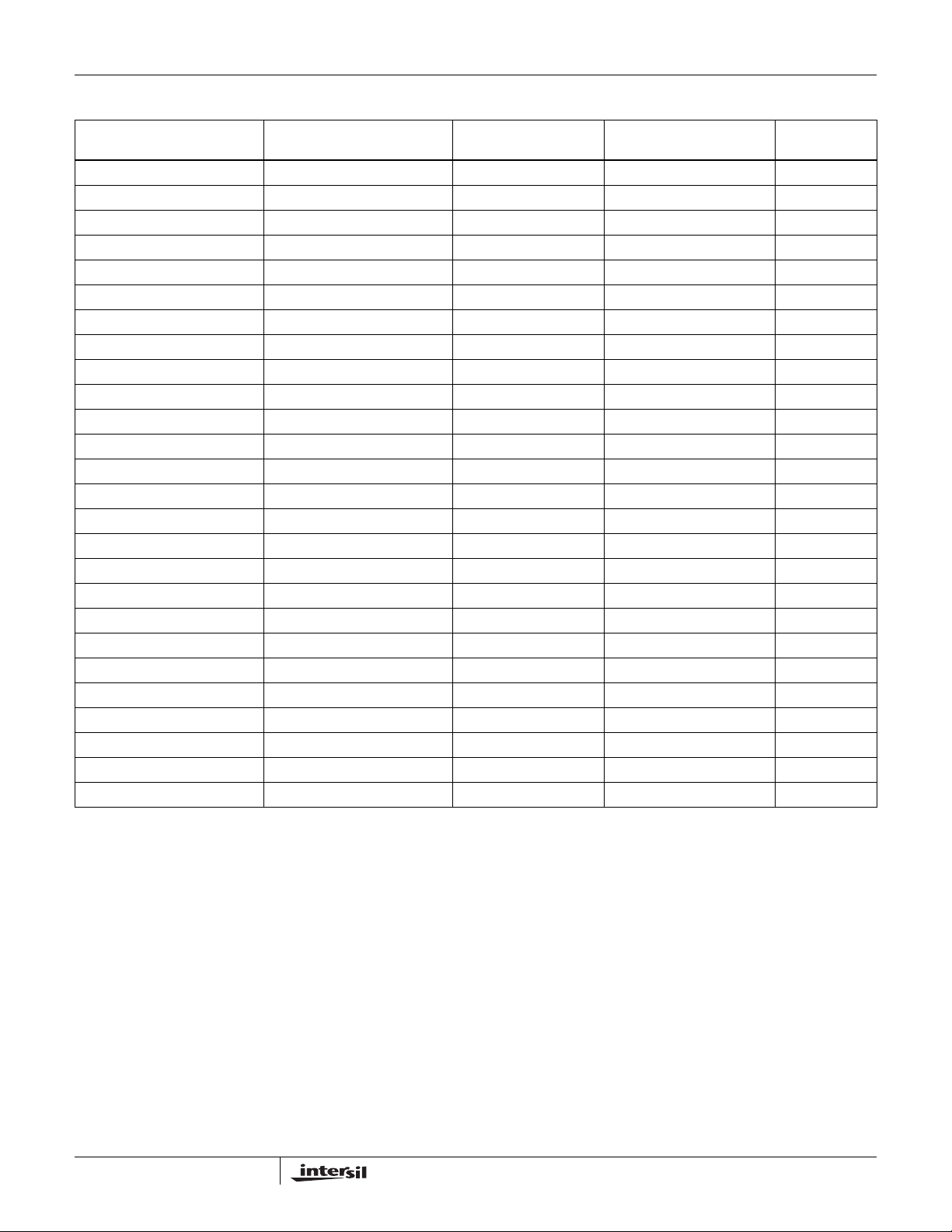
Ordering Information
TEMP.
PART NUMBER PART MARKING
HI1-0506-2 HI1-506-2 -55 to +125 28 Ld CERDIP F28.6
HI1-0506-5 HI1-506-5 0 to +75 28 Ld CERDIP F28.6
HI4P0506-5 HI4P 506-5 0 to +75 28 Ld PLCC N28.45
HI4P0506-5Z (Note 1) HI4P 506-5Z 0 to +75 28 Ld PLCC (Pb-free) N28.45
HI9P0506-5 HI9P506-5 0 to +75 28 Ld SOIC M28.3
HI9P0506-9 HI9P506-9 -40 to +85 28 Ld SOIC M28.3
HI9P0506-9Z (Note 1) HI9P506-9Z -40 to +85 28 Ld SOIC (Pb-free) M28.3
HI1-0507-2 HI1-507-2 -55 to +125 28 Ld CERDIP F28.6
HI3-0507-5 HI3-507-5 0 to +75 28 Ld PDIP E28.6
HI3-0507-5Z HI3-507-5Z 0 to +75 28 Ld PDIP (Note 3) (Pb-free) E28.6
HI1-0508-2 HI1-508-2 -55 to 125 16 Ld CERDIP F16.3
HI1-0508-5 HI1-508 0 to +75 16 Ld CERDIP F16.3
HI3-0508-5 HI3-508-5 0 to +75 16 Ld PDIP E16.3
HI3-0508-5Z (Note 1) HI3-508-5Z 0 to +75 16 Ld PDIP (Note 3) (Pb-free) E16.3
HI9P0508-5 HI9P508-5 0 to +75 16 Ld SOIC M16.15
HI9P0508-5Z (Notes 1, 2) HI9P508-5Z 0 to +75 16 Ld SOIC (Pb-free) M16.15
HI9P0508-9 HI9P508-9 -40 to +85 16 Ld SOIC M16.15
HI9P0508-9Z (Note 1) HI9P508-9Z -40 to +85 16 Ld SOIC (Pb-free) M16.15
HI1-0509-2 HI1-509-2 -55 to +125 16 Ld CERDIP F16.3
HI1-0509-4 HI1-509-4 -25 to +85 16 Ld CERDIP F16.3
HI1-0509-5 HI1-509-5 0 to +75 16 Ld CERDIP F16.3
HI3-0509-5 HI3-509-5 0 to +75 16 Ld PDIP E16.3
HI4P0509-5 HI4P 509-5 0 to +75 20 Ld PLCC N20.35
HI4P0509-5Z (Notes 1, 2) HI4P 509-5Z 0 to +75 20 Ld PLCC (Pb-free) N20.35
HI9P0509-5 HI9P 509-5 0 to +75 16 Ld SOIC M16.15
HI9P0509-5Z (Notes 1, 2) HI9P 509-5Z 0 to +75 16 Ld SOIC (Pb-free) M16.15
NOTES:
1. These Intersil Pb-free plastic packaged products employ special Pb-free material sets; molding compounds/die attach materials and 100% matte
tin plate PLUS ANNEAL - e3 termination finish, which is RoHS compliant and compatible with both SnPb and Pb-free soldering operations.
Intersil Pb-free products are MSL classified at Pb-free peak reflow temperatures that meet or exceed the Pb-free requirements of IPC/JEDEC
J STD-020.
2. Add “96” suffix for tape and reel. Please refer to TB347 for details on reel specifications.
3. Pb-free PDIPs can be used for through hole wave solder processing only. They are not intended for use in Reflow solder processing applications.
RANGE (°C) PACKAGE PKG. DWG. #
2
FN3142.8
October 30, 2007
Page 3
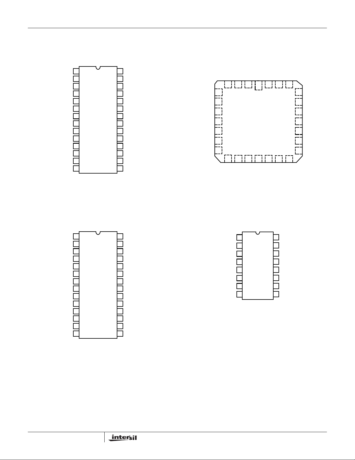
Pinouts
ADDRESS A
+V
HI-506 (CERDIP, SOIC)
NC
NC
IN 16
IN 15
IN 14
IN 13
IN 12
IN 11
IN 10
IN 9
GND
NC
1
2
3
4
5
6
7
8
9
10
11
12
13
14
3
SUPPLY
TOP VIEW
HI-506, HI-507, HI-508, HI-509
28
OUT
-V
27
SUPPLY
IN 8
26
IN 7
25
IN 6
24
IN 5
23
IN 4
22
IN 3
21
20
IN 2
IN 1
19
ENABLE
18
ADDRESS A
17
16
ADDRESS A
ADDRESS A
15
0
1
2
IN 15
IN 14
IN 13
IN 12
IN 11
IN 10
IN 9
HI-506 (PLCC)
TOP VIEW
IN 16
NC
3214282726
5
6
7
8
9
10
11
NC
GND
SUPPLY
NC
+V
14 15 16 17 1812 13
3A2A1
A
OUT
SUPPLY
-V
0
A
IN 8
25
IN 7
24
IN 6
23
IN 5
22
IN 4
21
IN 3
IN 2
20
IN 1
19
ENABLE
+V
HI-507 (PDIP, CERDIP)
OUT B
NC
IN 8B
IN 7B
IN 6B
IN 5B
IN 4B
IN 3B
IN 2B
IN 1B
GND
NC
NC
1
2
3
4
5
6
7
8
9
10
11
12
13
14
SUPPLY
TOP VIEW
28
OUT A
-V
27
SUPPLY
IN 8A
26
IN 7A
25
IN 6A
24
23
IN 5A
IN 4A
22
21
IN 3A
20
IN 2A
19
IN 1A
18
ENABLE
17
ADDRESS A
16
ADDRESS A
ADDRESS A
15
HI-508 (PDIP, CERDIP, SOIC)
TOP VIEW
A
1
A
0
IN 1
IN 2
IN 3
IN 4
OUT
2
3
4
5
6
7
8
ENABLE
-V
SUPPLY
0
1
2
16
1
15
A
2
14
GND
+V
13
SUPPLY
12
IN 5
11
IN 6
10
IN 7
9
IN 8
3
FN3142.8
October 30, 2007
Page 4
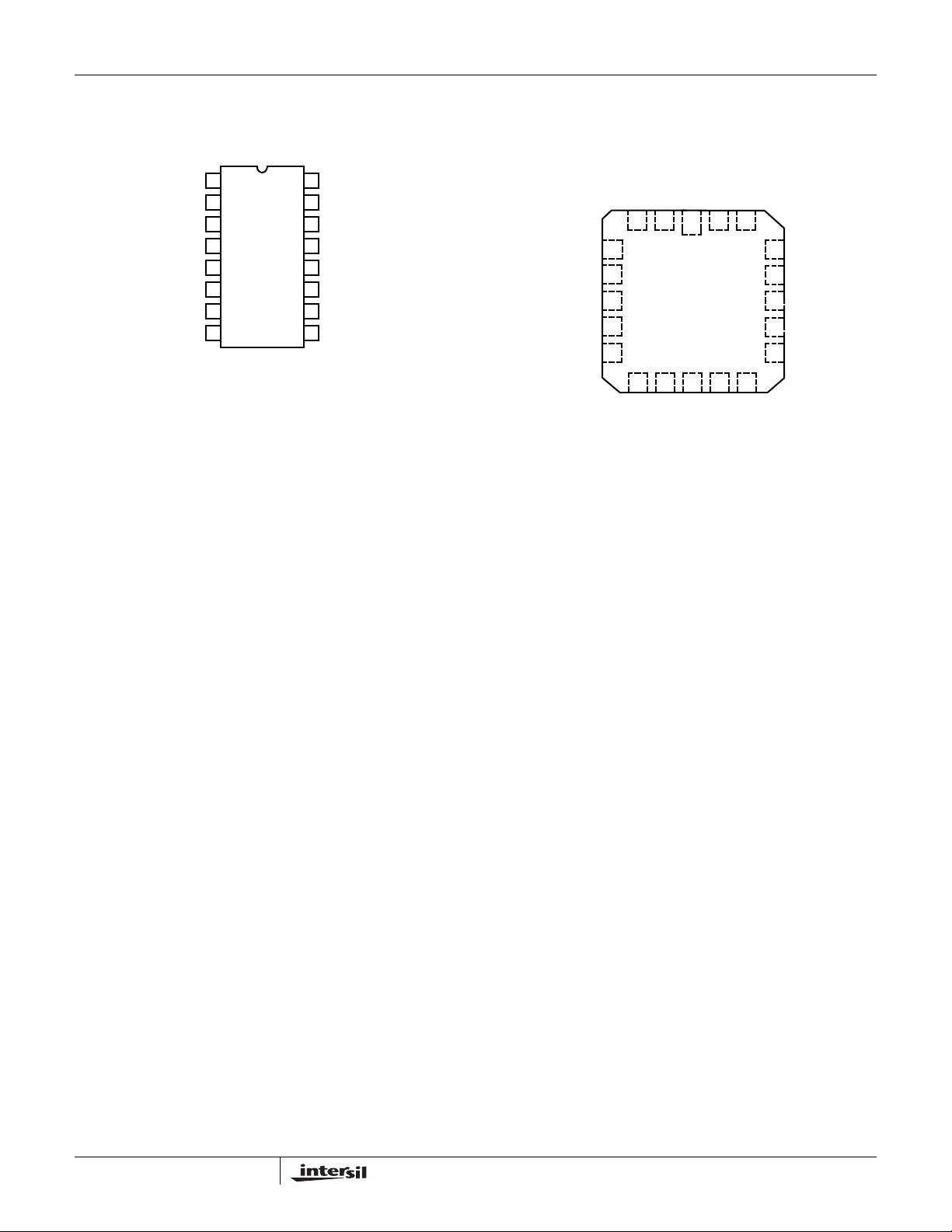
Pinouts (Continued)
HI-509 (PDIP, CERDIP, SOIC)
1
A
0
IN 1A
IN 2A
IN 3A
IN 4A
OUT A
2
3
4
5
6
7
8
ENABLE
-V
SUPPLY
TOP VIEW
HI-506, HI-507, HI-508, HI-509
A
16
1
GND
15
14
+V
SUPPLY
13
IN 1B
IN 2B
12
IN 3B
11
IN 4B
10
OUT B
9
-V
SUPPLY
IN 1A
NC
IN 2A
IN 3A
HI-509 (PLCC)
TOP VIEW
0
ENABLE
A
NC
3212019
4
5
6
7
8
10 11 12 139
1
A
GND
+V
18
SUPPLY
IN 1B
17
NC
16
IN 2B
15
IN 3B
14
IN 4A
NC
OUT A
IN 4B
OUT B
4
FN3142.8
October 30, 2007
Page 5
HI-506, HI-507, HI-508, HI-509
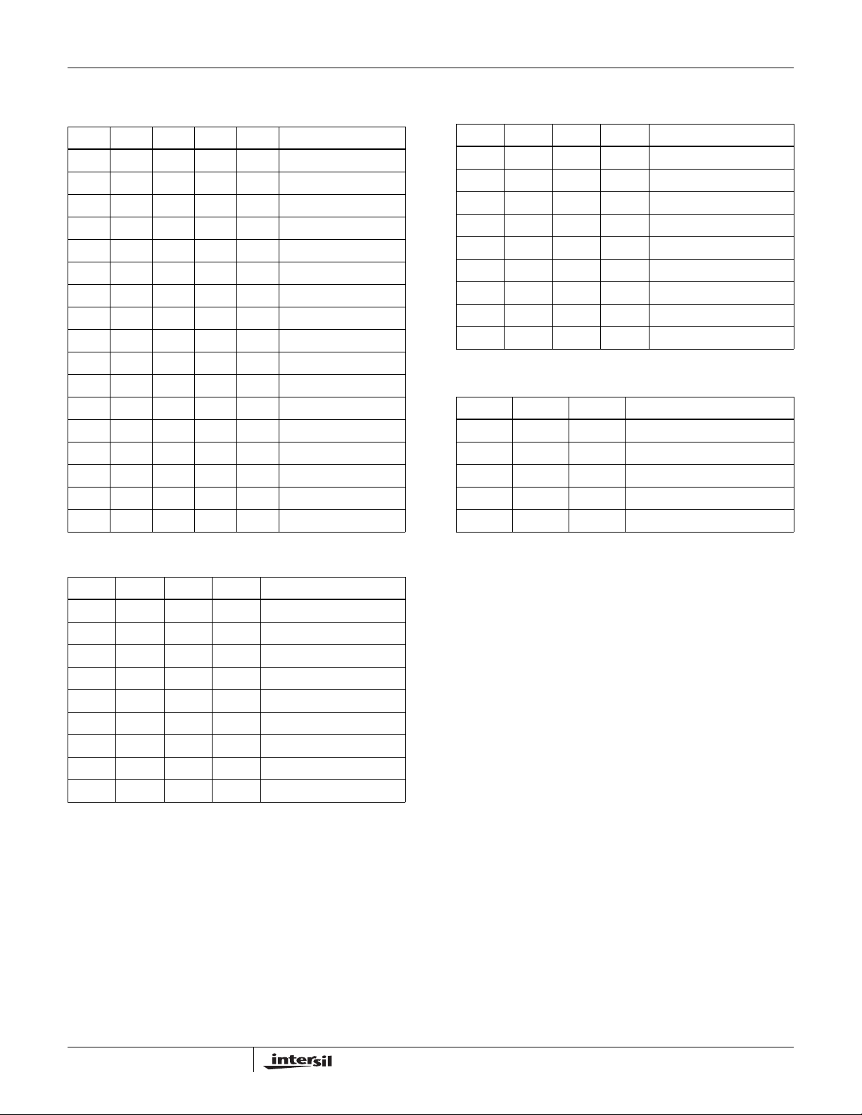
Truth Ta bles
HI-506
A
A
3
A
2
A
1
EN “ON” CHANNEL
0
XXXXL None
LLLLH 1
LLLHH 2
LLHLH 3
LLHHH 4
LHLLH 5
LHLHH 6
LHHLH 7
LHHHH 8
HLLLH 9
HLLHH 10
HLHLH 11
HLHHH 12
HHL LH 13
HHLHH 14
HHHLH 15
HHHHH 16
HI-508
A
A
2
A
1
EN “ON” CHANNEL
0
X X X L None
LLLH 1
LLHH 2
LHLH 3
LHHH 4
HLLH 5
HLHH 6
HHLH 7
HHHH 8
HI-509
A
1
A
0
EN “ON” CHANNEL PAIR
X X L None
LLH 1
LHH 2
HLH 3
HHH 4
HI-507
A
A
2
A
1
EN “ON” CHANNEL
0
X X X L None
LLLH 1
LLHH 2
LHLH 3
LHHH 4
HLLH 5
HLHH 6
HHLH 7
HHHH 8
5
FN3142.8
October 30, 2007
Page 6
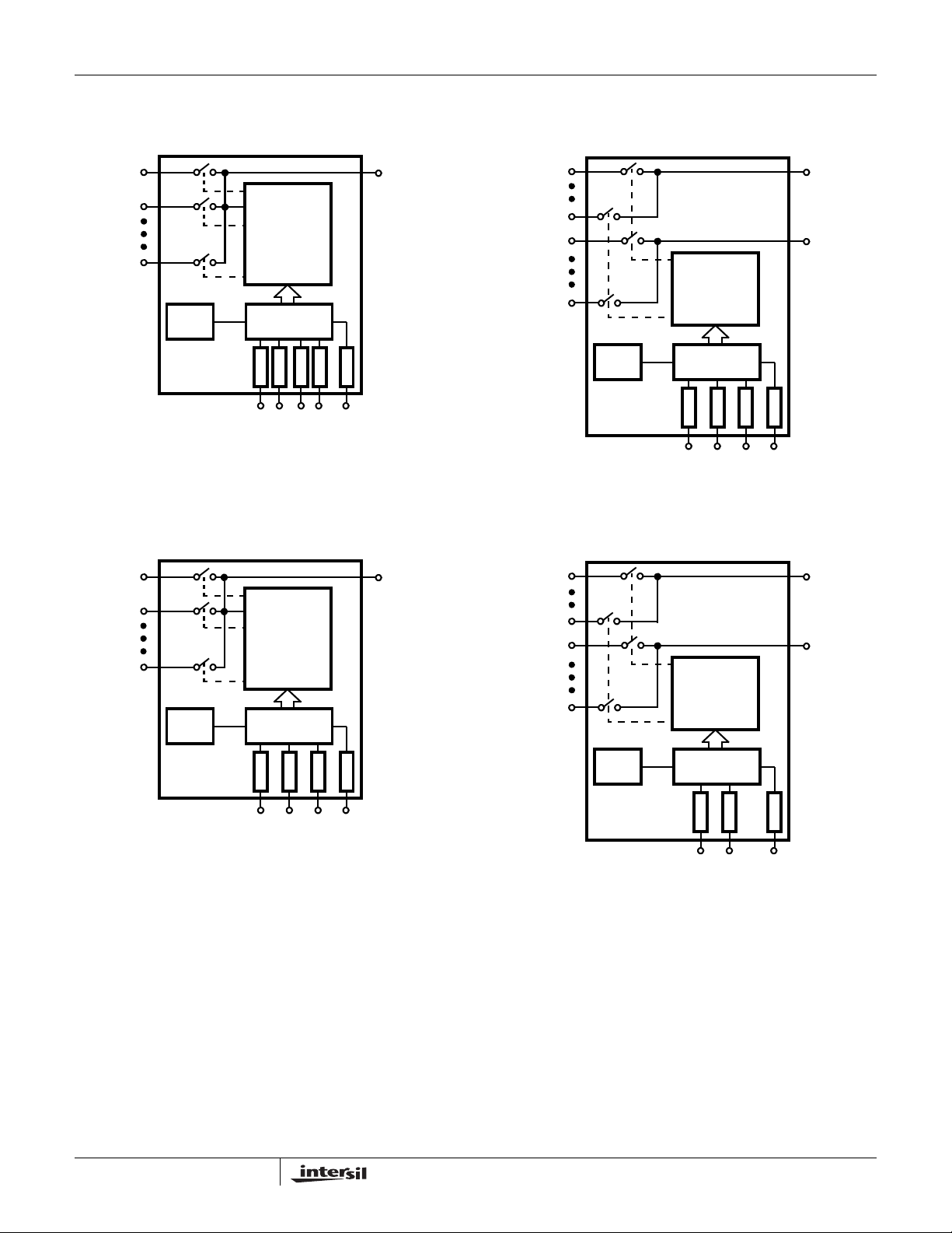
Functional Diagrams
HI-506 HI-507
HI-506, HI-507, HI-508, HI-509
IN 1
IN 2
IN 16
IN 1
IN 2
IN 8
5V
REF
DIGITAL
†
INPUT
PROTECTION
5V
REF
IN 1A
IN 8A
IN 1B
IN 8B
5V
REF
DIGITAL
†
INPUT
PROTECTION
DECODER/
DRIVER
† † †
A
0A1A2
DECODER/
DRIVER
LEVEL
SHIFT
† † † †
A
0A1A2A3
OUT
†
EN
HI-508 HI-509
IN 1A
IN 4A
IN 1B
IN 4B
DECODER/
DRIVER
DECODER/
DRIVER
LEVEL
SHIFT
OUT
LEVEL
SHIFT
OUT A
OUT B
†
EN
OUT A
OUT B
DIGITAL
†
INPUT
PROTECTION
† † †
A
0A1A2
6
EN
5V
†
REF
DIGITAL
†
INPUT
PROTECTION
LEVEL
SHIFT
† †
A
0A1
†
EN
FN3142.8
October 30, 2007
Page 7
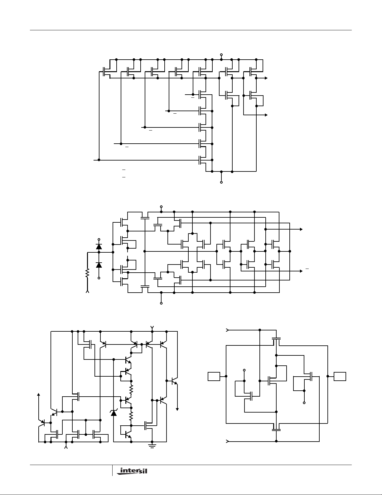
HI-506, HI-507, HI-508, HI-509
Schematic Diagrams
ENABLE
DELETE A
DELETE A
V+
D1
ADDRESS DECODER
P
PP PP P P
A1 OR A
A2 OR A
2
A3 OR A
3
OR A3 INPUT FOR HI-507, HI-508, HI-509
3
OR A2 INPUT FOR HI-509
2
ADDRESS INPUT BUFFER LEVEL SHIFTER
P3
P1
N1
V+
P5
P4
A
1
OR A
0
P6
V+
N
0
N
N
N
N
P7
NN
V-
P8 P9 P10
TO P-CHANNEL
DEVICE OF
THE SWITCH
TO N-CHANNEL
DEVICE OF
THE SWITCH
A
Q9P
V
L
Q10N
200Ω
TTL REFERENCE CIRCUIT MULTIPLEX SWITCH
N13 N14
A
N12
IN
P15
N15
D2
V
L
V
R
P2
V-
Q1P
D3
N2
Q2PV+Q3P Q4P
Q5N
Q6N
R2
16.8k
Q11P
R3
6.8k
Q12N
N3
N4
P16
N5
V-
Q8N
Q7P
V
R
N7
N6
ALL N-CHANNEL BODIES TO VALL P-CHANNEL BODIES TO V+
UNLESS OTHERWISE INDICATED
N8 N9 N10
FROM DECODE
IN
V+
P17
N19
P18
A
N18
N17
OUT
V-
V- GND
7
FROM DECODE
FN3142.8
October 30, 2007
Page 8
HI-506, HI-507, HI-508, HI-509
Absolute Maximum Ratings Thermal Information
V+ to V- . . . . . . . . . . . . . . . . . . . . . . . . . . . . . . . . . . . . . . . . . . .+44V
V+ to GND . . . . . . . . . . . . . . . . . . . . . . . . . . . . . . . . . . . . . . . . .+22V
V- to GND. . . . . . . . . . . . . . . . . . . . . . . . . . . . . . . . . . . . . . . . . -25V
Digital Input Voltage (V
Analog Signal (V
IN
, VA) . . . . . (V-) -4V to (V+) +4V or 20mA,
EN
, V
, Note 5) . . . . . . . . . .(V-) -2V to (V+) +2V
OUT
Whichever Occurs First
Continuous Current, In or Out . . . . . . . . . . . . . . . . . . . . . . . . . 20mA
Peak Current, In or Out (Pulsed 1ms, 10% Duty Cycle Max) . 40mA
Operating Conditions
Temperature Ranges
HI-50X-2. . . . . . . . . . . . . . . . . . . . . . . . . . . . . . . .-55°C to +125°C
HI-50X-4. . . . . . . . . . . . . . . . . . . . . . . . . . . . . . . . .-25°C to +85°C
HI-50X-5. . . . . . . . . . . . . . . . . . . . . . . . . . . . . . . . . . 0°C to +75°C
HI-50X-9. . . . . . . . . . . . . . . . . . . . . . . . . . . . . . . . .-40°C to +85°C
Typical Minimum Supply Voltage. . . . . . . . . . . . ± 10V or Single 20V
CAUTION: Do not operate at or near the maximum ratings listed for extended periods of time. Exposure to such conditions may adversely impact product reliability and
result in failures not covered by warranty.
NOTE:
is measured with the component mounted on a low effective thermal conductivity test board in free air. See Tech Brief TB379 for details.
4. θ
JA
5. Signals on IN or OUT exceeding V+ or V- are clamped by internal diodes. Limit resulting current to maximum current ratings. If an overvoltage
condition is anticipated (analog input exceeds either power supply voltage), the Intersil HI-546/HI-547/HI-548/HI-549 multiplexers are
recommended.
Thermal Resistance (Typical, Note 4) θ
(°C/W) θJC (°C/W)
JA
16 Ld CERDIP Package. . . . . . . . . . . . 85 32
16 Ld SOIC Package . . . . . . . . . . . . . . 115 N/A
16 Ld PDIP Package . . . . . . . . . . . . . . 100 N/A
20 Ld PLCC Package. . . . . . . . . . . . . . 80 N/A
28 Ld CERDIP Package. . . . . . . . . . . . 55 18
28 Ld PDIP Package . . . . . . . . . . . . . . 60 N/A
28 Ld SOIC Package . . . . . . . . . . . . . . 70 N/A
28 Ld PLCC Package. . . . . . . . . . . . . . 70 N/A
Maximum Junction Temperature
Ceramic Packages. . . . . . . . . . . . . . . . . . . . . . . . . . . . . . . +175°C
Plastic Packages . . . . . . . . . . . . . . . . . . . . . . . . . . . . . . . .+150°C
Maximum Storage Temperature Range. . . . . . . . . .-65°C to +150°C
Pb-free reflow profile . . . . . . . . . . . . . . . . . . . . . . . . . .see link below
http://www.intersil.com/pbfree/Pb-FreeReflow.asp
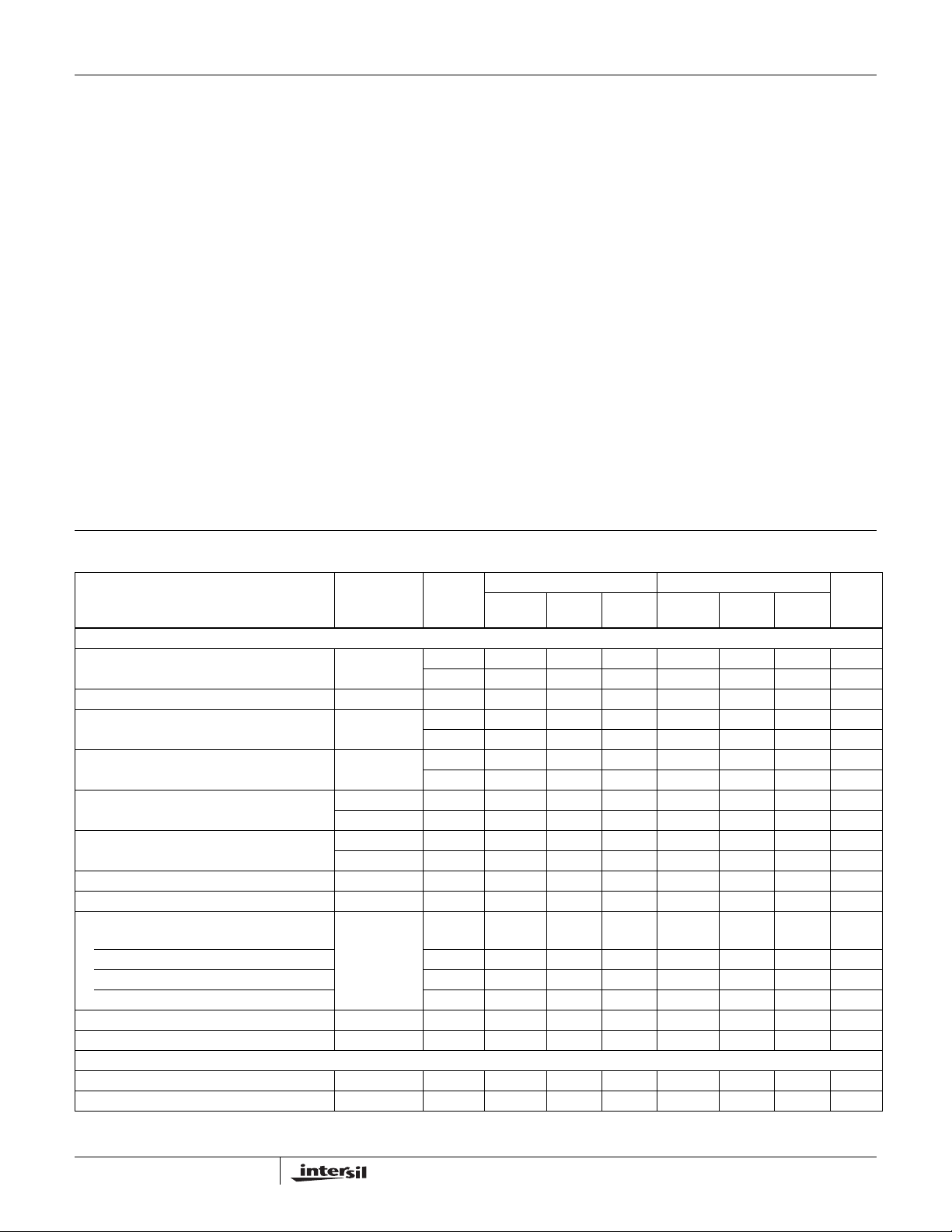
Electrical Specifications Supplies = +15V, -15V; V
Unless Otherwise Specified. For Test Conditions, Consult Test Circuits Section
(Logic Level High) = 2.4V; VAL (Logic Level Low) = 0.8V,
AH
-2 -4, -5, -9
PARAMETER
TEST
CONDITIONS
TEMP
(°C)
MIN
(Note 11) TYP MAX
MIN
(Note 11) TYP MAX
UNITS
DYNAMIC CHARACTERISTICS
Access Time, t
A
25 - 250 500 - 250 - ns
Full - - 1000 - - 1000 ns
Break-Before-Make Delay, t
Enable Delay (ON), t
ON(EN)
OPEN
25 25 80 - 25 80 - ns
25 - 250 500 - 250 - ns
Full - - 1000 - - 1000 ns
Enable Delay (OFF), t
OFF(EN)
25 - 250 500 - 250 - ns
Full - - 1000 - - 1000 ns
Settling Time, t
S
(HI-506 and HI-507)
Settling Time, t
(HI-508 and HI-509)
S
To 0.1% 25 - 1.2 - - 1.2 - μs
To 0.01% 25 - 2.4 - - 2.4 - μs
To 0.1% 25 - 360 - - 360 - ns
To 0.01% 25 - 600 - - 600 - ns
Off Isolation Note 9 25 - 68 - - 68 - dB
Channel Input Capacitance, C
Channel Output Capacitance, C
S(OFF)
D(OFF)
25 -10- -10-pF
HI-506 25 -52- -52-pF
HI-507 25 -30- -30-pF
HI-508 25 -17- -17-pF
HI-509 25 -12- -12-pF
Digital Input Capacitance, C
A
Input to Output Capacitance, C
DS(OFF)
25 - 6 - - 6 - pF
25 -0.08- -0.08-pF
DIGITAL INPUT CHARACTERISTICS
Input Low Threshold, V
Input High Threshold, V
AL
AH
Full - - 0.8 - - 0.8 V
Full 2.4 - - 2.4 - - V
8
FN3142.8
October 30, 2007
Page 9
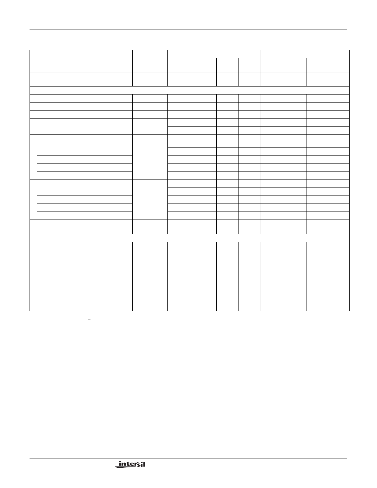
HI-506, HI-507, HI-508, HI-509
Electrical Specifications Supplies = +15V, -15V; V
Unless Otherwise Specified. For Test Conditions, Consult Test Circuits Section (Continued)
(Logic Level High) = 2.4V; VAL (Logic Level Low) = 0.8V,
AH
-2 -4, -5, -9
PARAMETER
Input Leakage Current
(High or Low), I
A
TEST
CONDITIONS
Note 8 Full - - 1.0 - - 1.0 μA
TEMP
(°C)
MIN
(Note 11) TYP MAX
MIN
(Note 11) TYP MAX
UNITS
ANALOG CHANNEL CHARACTERISTICS
Analog Signal Range, V
On Resistance, r
, (Any Two Channels)25-5--5-%
Δr
ON
Off Input Leakage Current, I
ON
IN
Note 6 25 - 180 300 - 180 400 Ω
Note 7 25 - 0.03 - - 0.03 - nA
S(OFF)
Full -15 - +15 -15 - +15 V
Full - - 50 - - 50 nA
Off Output Leakage Current,
)
I
D(OFF
Note 7 25 - 0.3 - - 0.3 - nA
HI-506 Full - - 300 - - 300 nA
HI-507 Full - - 200 - - 200 nA
HI-508 Full - - 200 - - 200 nA
HI-509 Full - - 100 - - 100 nA
On Channel Leakage Current, I
Note 7 25 - 0.3 - - 0.3 - nA
D(ON)
HI-506 Full - - 300 - - 300 nA
HI-507 Full - - 200 - - 200 nA
HI-508 Full - - 200 - - 200 nA
HI-509 Full - - 100 - - 100 nA
Differential Off Output Leakage Current, I
DIFF
Full - - 50 - - 50 nA
(HI-507, HI-509 Only)
POWER SUPPLY CHARACTERISTICS
Current, I+
HI-506/HI-507 Note 10 Full - 1.5 3.0 - 1.5 3.0 mA
HI-508/HI-509 Note 10 Full - 1.5 2.4 - 1.5 2.4 mA
Current, I-
HI-506/HI-507 Note 10 Full - 0.4 1.0 - 0.4 1.0 mA
HI-508/HI-509 Note 10 Full - 0.4 1.0 - 0.4 1.0 mA
Power Dissipation, P
D
HI-506/HI-507 Full - - 60 - - 60 mW
HI-508/HI-509 Full - - 51 - - 51 mW
NOTES:
6. V
OUT
= ±10V, I
OUT
= +1mA.
7. 10nA is the practical lower limit for high speed measurement in the production test environment.
8. Digital input leakage is primarily due to the clamp diodes (see Schematic). Typical leakage is less than 1nA at +25°C.
9. V
10. V
= 0.8V, RL = 1k, CL = 15pF, VS = 7V
EN
, VA = 0V or 2.4V.
EN
, f = 100kHz.
RMS
11. Parts are 100% tested at +25°C. Over-temperature limits established by characterization and are not production tested.
9
FN3142.8
October 30, 2007
Page 10
HI-506, HI-507, HI-508, HI-509
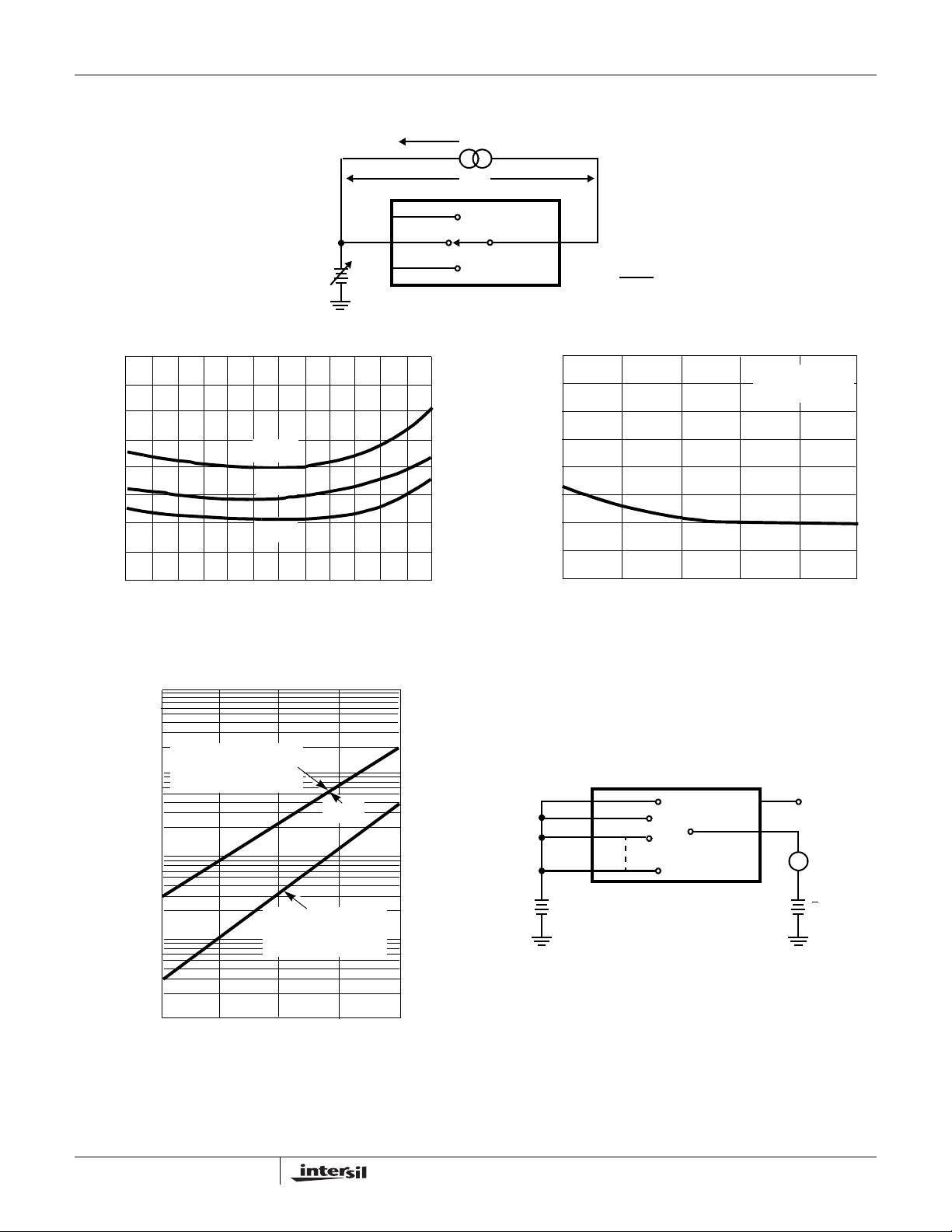
Test Circuits and Waveforms T
400
300
+125°C
200
+25°C
ON RESISTANCE (Ω)
100
-55°C
= +25°C, V
A
V
IN
= ±15V, VAH = 2.4V , VAL = 0.8V , Unless Otherwise Specified
SUPPLY
1mA
V
2
FIGURE 1A. TEST CIRCUIT
2.2
2.0
1.8
1.6
1.4
1.2
1.0
NORMALIZED RESISTANCE
0.8
(REFERRED TO VALUE AT ±15V)
OUTIN
V
1mA
2
-55°C TO +125°C
= 0V
V
IN
rON =
0
-15
-10 -5 0 5 10 15
ANALOG INPUT (V)
FIGURE 1B. ON RESISTANCE vs ANALOG INPUT VOLTAGE
FIGURE 1. ON RESISTANCE
100nA
OFF OUTPUT
10nA
1nA
LEAKAGE CURRENT
100pA
10pA
LEAKAGE CURRENT
25 50 75 100 125
I
D(OFF)
OFF INPUT
LEAKAGE CURRENT
I
S(OFF)
TEMPERATURE (°C)
I
D(ON)
FIGURE 2A. LEAKAGE CURRENT vs TEMPERATURE
0.6
10 11 12 13 14 15
SUPPLY VOLTAGE (±V)
FIGURE 1C. NORMALIZED ON RESISTANCE vs SUPPL Y
VOLTAGE
OUT
0.8V
A
I
D(OFF)
+10V
±10V
FIGURE 2B. I
EN
TEST CIRCUIT (NOTE 12)
D(OFF)
10
FN3142.8
October 30, 2007
Page 11
HI-506, HI-507, HI-508, HI-509
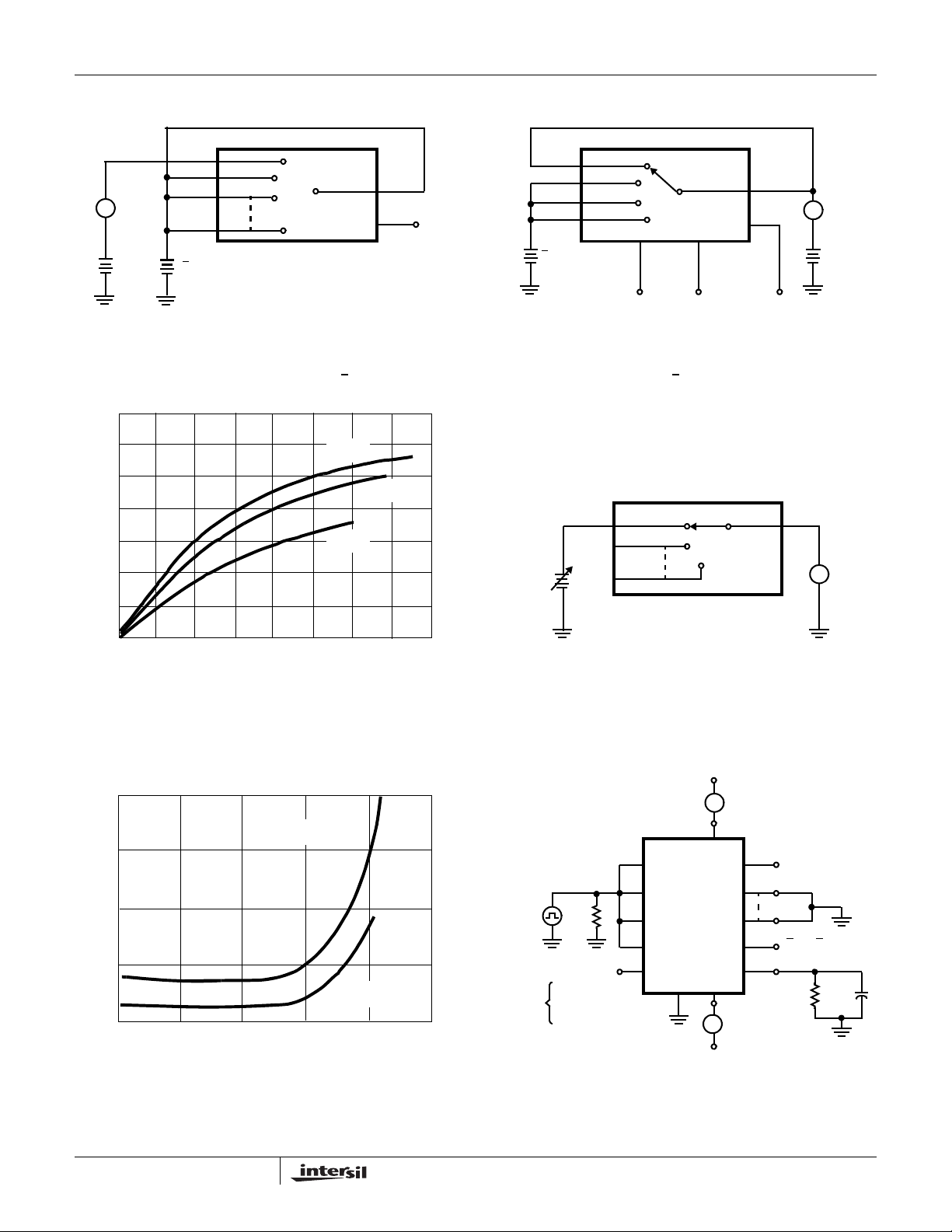
Test Circuits and Waveforms T
I
A
S(OFF)
±10V
FIGURE 2C. I
NOTE:
12. Two measurements per channel: ±10V and +
70
60
50
40
30
+10V
TEST CIRCUIT (NOTE 12)
S(OFF)
-55°C
+125°C
= +25°C, V
A
EN
OUT
= ±15V, VAH = 2.4V , VAL = 0.8V , Unless Otherwise Specified (Continued)
SUPPLY
0.8V
FIGURE 2. LEAKAGE CURRENTS
10V. (Two measurements per device for I
+25°C
+10V
FIGURE 2D. I
D(OFF)
A
0
D(ON)
A
TEST CIRCUIT (NOTE 12)
±10V and +10V)
OUT
A
I
EN
1
2.4V
D(ON)
±10V
20
SWITCH CURRENT (mA)
10
0
024 6810121416
VOLTAGE ACROSS SWITCH (±V)
±V
IN
FIGURE 3A. ON CHANNEL CURRENT vs VOLTAGE FIGURE 3B. TEST CIRCUIT
FIGURE 3. ON CHANNEL CURRENT
8
V
= ±15V
SUPPLY
6
4
SUPPLY CURRENT (mA)
2
V
= ±10V
SUPPLY
0
1k
10k 100k 1M 10M
TOGGLE FREQUENCY (Hz)
†
Similar connection for HI-507/
HI-508/HI-509
V
A
HIGH = 3.5V
LOW = 0V
V
A
50% DUTY CYCLE
50Ω
3.5V
A
A
A
A
EN
3
2
1
0
HI-506
GND
A
V+
IN 1
†
IN 2
THRU
IN 7/15
IN 8/16
OUT
V-
A
+15V/+10V
+I
SUPPLY
-I
SUPPLY
-15V/-10V
A
±10V/±5V
+10V/+5V
10
MΩ
14
pF
FIGURE 4A. SUPPLY CURRENT vs TOGGLE FREQUENCY FIGURE 4B. TEST CIRCUIT
FIGURE 4. DYNAMIC SUPPLY CURRENT
11
FN3142.8
October 30, 2007
Page 12
HI-506, HI-507, HI-508, HI-509
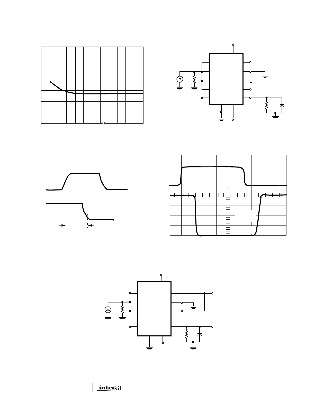
Test Circuits and Waveforms T
600
400
200
ACCESS TIME (ns)
0
2
345 151413
LOGIC LEVEL (HIGH) (V)
= +25°C, V
A
= ±15V, VAH = 2.4V , VAL = 0.8V , Unless Otherwise Specified (Continued)
SUPPLY
A
3
IN 2 THRU
A
2
50Ω
V
A
3.5V
†
Similar connection for HI-507/
HI-508/HI-509
A
A
EN
1
0
HI-506
GND
FIGURE 5A. ACCESS TIME vs LOGIC LEVEL (HIGH) FIGURE 5B. TEST CIRCUIT
3.5V
50%
ADDRESS
DRIVE (V
)
A
0V
VA INPUT
2V/DIV.
S1 ON
+15V
V+
IN 1
IN 7/15
†
IN 16
OUT
V-
-15V
±10V
+10V
10
kΩ
50
pF
+10V
OUTPUT
10%
t
A
FIGURE 5C. MEASUREMENT POINTS
V
A
Similar connection for HI-507/HI-508/HI-509
†
-10V
50Ω
FIGURE 5. ACCESS TIME
A
3
HI-506†
A
2
A
1
A
0
3.5V
EN
GND
+15V
V+
IN 1
IN 2 THRU
IN 7/IN 15
IN 8 /16
OUT
V-
-15V
200Ω
OUTPUT
5V/DIV.
S16 ON
200ns/DIV.
FIGURE 5D. WAVEFORMS
+5V
V
OUT
50pF
12
FIGURE 6A. TEST CIRCUIT
FN3142.8
October 30, 2007
Page 13
HI-506, HI-507, HI-508, HI-509
Test Circuits and Waveforms T
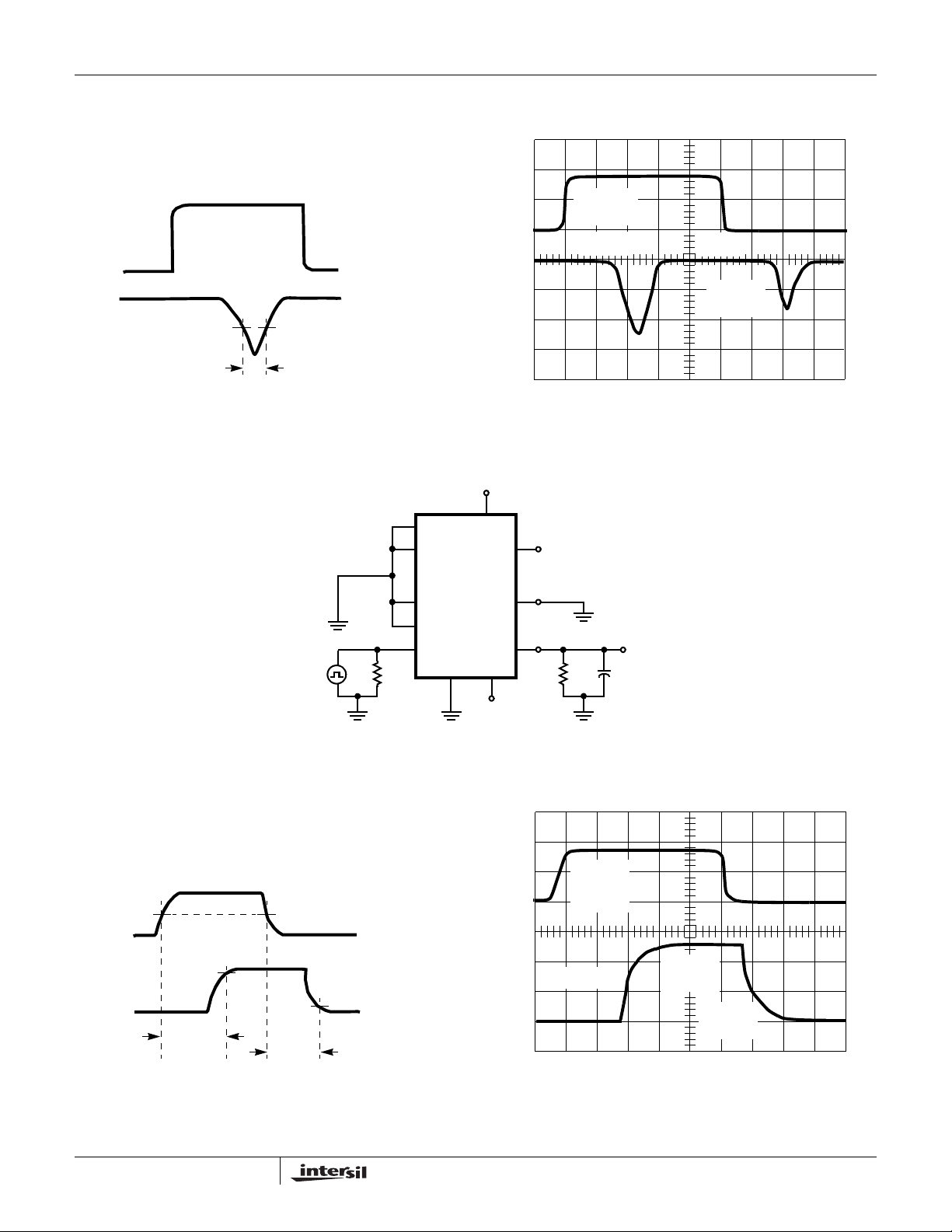
3.5V
ADDRESS
t
OPEN
DRIVE (V
V
A
0V
50% 50%
FIGURE 6B. MEASUREMENT POINTS
= +25°C, V
A
)
A
OUTPUT
= ±15V, VAH = 2.4V , VAL = 0.8V , Unless Otherwise Specified (Continued)
SUPPLY
FIGURE 6. BREAK-BEFORE-MAKE DELAY
+15V
HI-506†
IN 2 THRU
GND
V+
IN 1
IN 7/IN 15
IN 8 /16
OUT
V-
+10V
200Ω
50Ω
A
A
A
A
EN
3
2
1
0
VA INPUT
2V/DIV.
S1 ON
100ns/DIV.
FIGURE 6C. WAVEFORMS
V
OUT
50pF
S16 ON
OUTPUT
1V/DIV.
-15V
Similar connection for HI-507/HI-508/HI-509
†
FIGURE 7A. TEST CIRCUIT
ENABLE
DRIVE
2V/DIV.
DISABLED
ENABLED
(S
ON)
1
100ns/DIV
OUTPUT
2V/DIV.
50%
t
ON(EN)
90%
3.5V
ENABLE DRIVE (VA)
50%
t
OFF(EN)
10%
0V
OUTPUT
0V
FIGURE 7B. MEASUREMENT POINTS FIGURE 7C. WAVEFORMS
FIGURE 7. ENABLE DELAYS
13
FN3142.8
October 30, 2007
Page 14
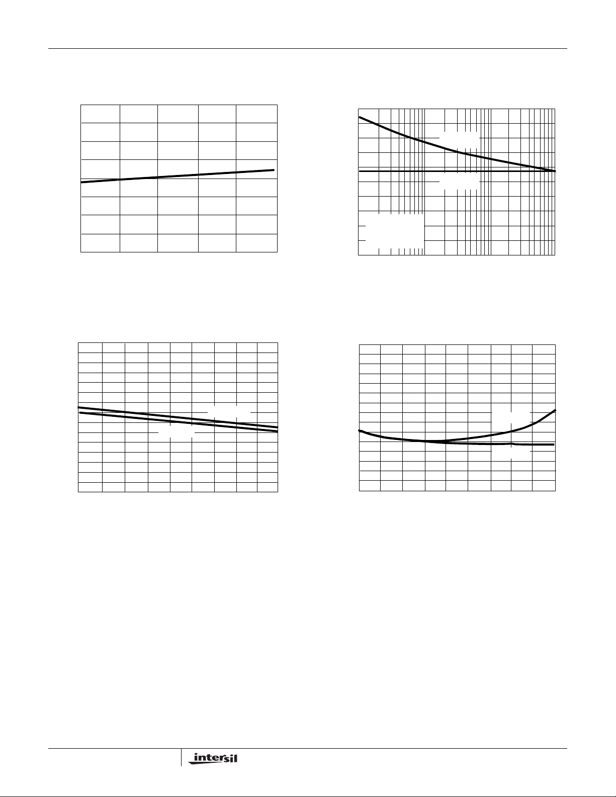
HI-506, HI-507, HI-508, HI-509
Typical Performance Curves T
4
3
2
1
INPUT LOGIC THRESHOLD (V)
0
10 12 14 16 18 20
POWER SUPPLY VOLTAGE (±V)
= 25°C, V
A
= ±15V , VAH = 2.4V, VAL = 0.8V , Un less Otherwise Specified
SUPPLY
100
80
60
40
) OFF ISOLATION (dB)
D
), (V
(V
S
VEN = 0V
20
C
= 28pF
LOAD
V
= 7V
S
RMS
0
4
10
5
10
FREQUENCY (Hz)
RL = 1k
RL = 10M
6
10
FIGURE 8. LOGIC THRESHOLD vs POWER SUPPLY VOLTAGE FIGURE 9. OFF ISOLATION vs FREQUENCY
3
3
7
10
2
VEN = 2.4V
VEN = 0V
1
POWER SUPPLY CURRENT (mA)
0
-55
-35 -15 -5 4525 65 85 105 125
TEMPERATURE (°C)
2
1
POWER SUPPLY CURRENT (mA)
0
-55
-35 -15 -5 25 45 65 85 105 125
EN = 5V
EN = 0V
TEMPERATURE (°C)
FIGURE 10A. HI-506/HI-507 FIGURE 10B. HI-508/HI-509
FIGURE 10. POWER SUPPLY CURRENT vs TEMPERATURE
14
FN3142.8
October 30, 2007
Page 15
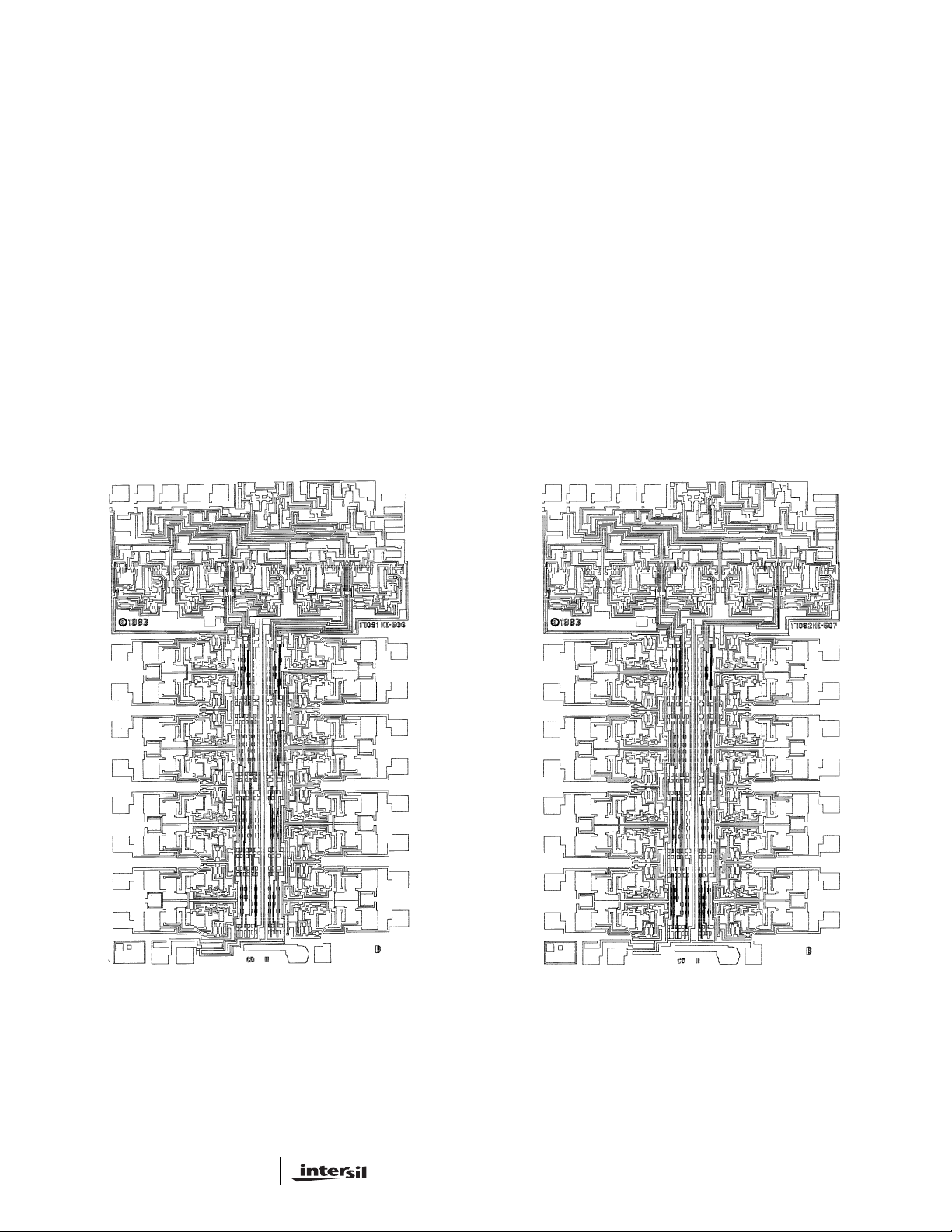
Die Characteristics
HI-506, HI-507, HI-508, HI-509
METALLIZATION:
Type: CuA l
Thickness: 16kÅ ±2kÅ
SUBSTRATE POTENTIAL (NOTE):
-V
SUPPLY
PASSIVATION:
Type: Nitride/Silox
Nitride Thickness: 3.5kÅ ±1kÅ
Silox Thickness: 12kÅ ±2kÅ
NOTE: The substrate appears resistive to the -V
conductor at -V
SUPPLY
potential.
Metallization Mask Layout
HI-506 HI-507
EN A0A1A
A
3
2
WORST CASE CURRENT DENSITY:
5
2
1.4 x 10
A/cm
TRANSISTOR COUNT:
421
PROCESS:
CMOS-DI
terminal, therefore it may be left floating (Insulating Die Mount) or it may be mounted on a
SUPPLY
GND
EN A
0A1A2
NC
GND
IN 1
IN 2
IN 3
IN 4
IN 5
IN 6
IN 7
IN 8
IN 9
IN 10
IN 11
IN 12
IN 13
IN 14
IN 15
IN 16
-V
OUT
+V
NC
IN 1A
IN 2A
IN 3A
IN 4A
IN 5A
IN 6A
IN 7A
IN 8A
-V
OUT A
+V
OUT B
IN 1B
IN 2B
IN 3B
IN 4B
IN 5B
IN 6B
IN 7B
IN 8B
15
FN3142.8
October 30, 2007
Page 16
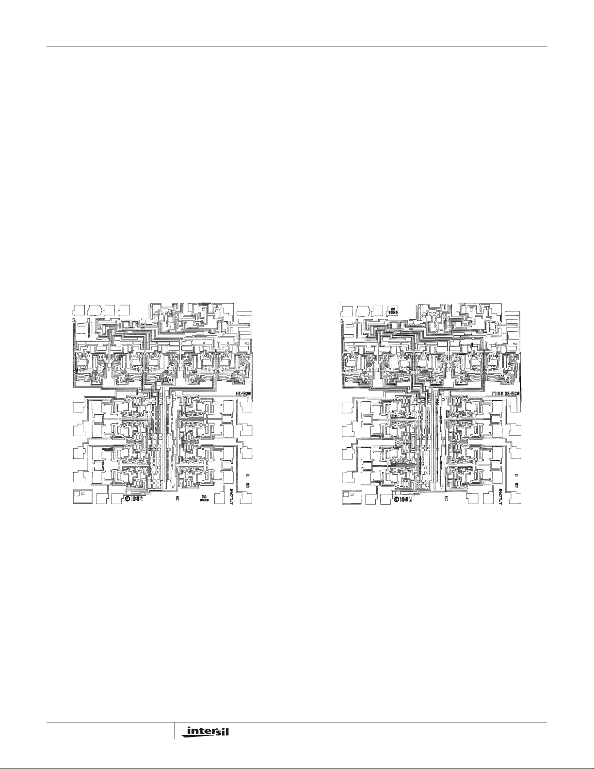
Die Characteristics
HI-506, HI-507, HI-508, HI-509
METALLIZATION:
Type: CuA l
Thickness: 16kÅ ±2kÅ
SUBSTRATE POTENTIAL (NOTE):
-V
SUPPLY
PASSIVATION:
Type: Nitride/Silox
Nitride Thickness: 3.5kÅ ±1kÅ
Silox Thickness: 12kÅ ±2kÅ
NOTE: The substrate appears resistive to the -V
conductor at -V
SUPPLY
potential.
Metallization Mask Layout
HI-508 HI-509
A
EN
0A1A2
WORST CASE CURRENT DENSITY:
5
2
1.4 x 10
A/cm
TRANSISTOR COUNT:
234
PROCESS:
CMOS-DI
terminal, therefore it may be left floating (Insulating Die Mount) or it may be mounted on a
SUPPLY
GND
EN
A
0A1
GND
-V
SUP
IN 1
IN 2
IN 3
IN 4
OUT IN 8
+V
IN 5
IN 6
IN 7
SUP
-V
SUP
IN 1A
IN 2A
IN 3A
OUT A IN 4B
IN 4A
OUT B
+V
IN 1B
IN 2B
IN 3B
SUP
16
FN3142.8
October 30, 2007
Page 17
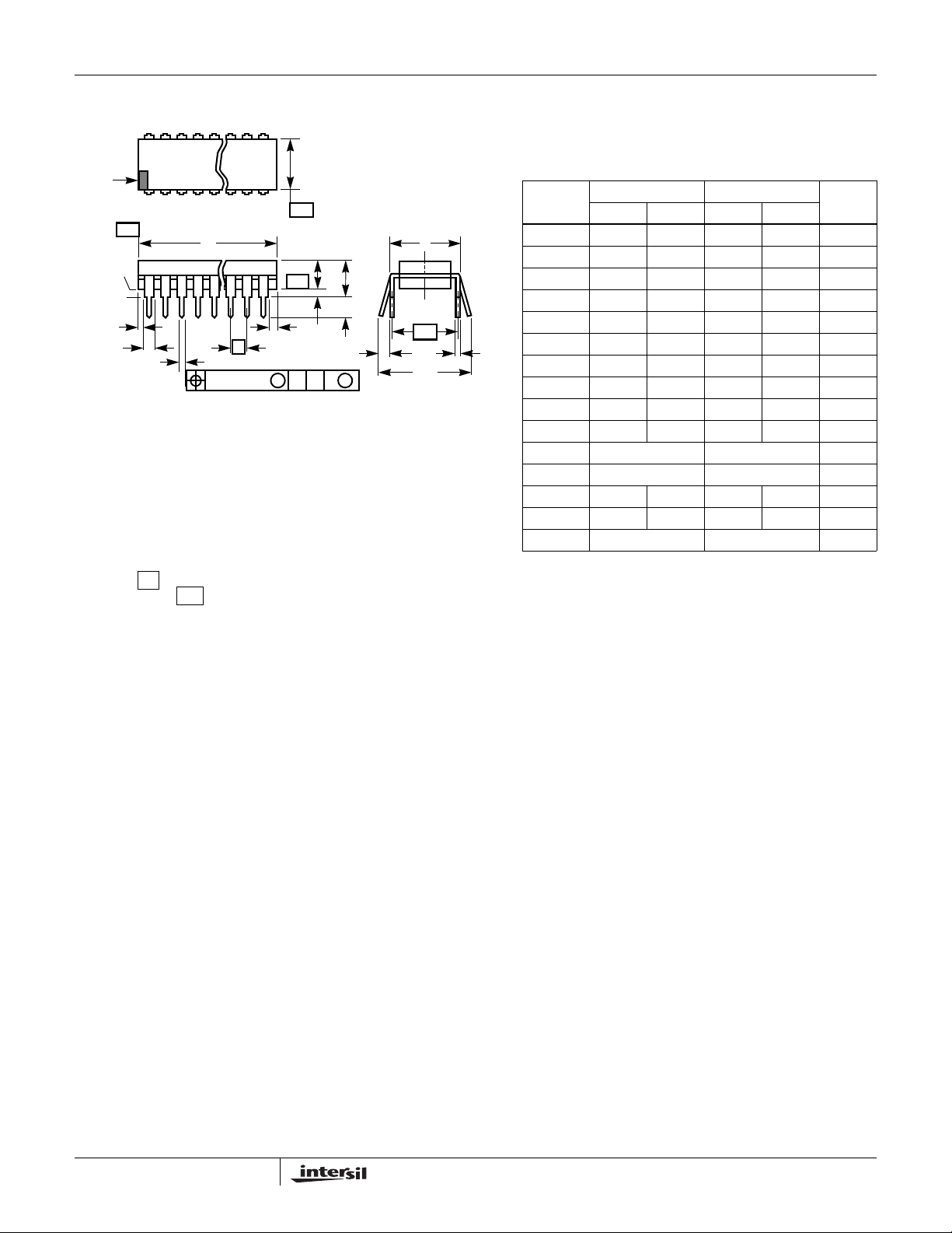
HI-506, HI-507, HI-508, HI-509
Dual-In-Line Plastic Packages (PDIP)
N
D1
-C-
E1
-B-
A1
A2
E
A
L
e
C
C
L
e
A
C
e
B
INDEX
AREA
BASE
PLANE
SEATING
PLANE
D1
B1
12 3 N/2
-AD
e
B
0.010 (0.25) C AM BS
NOTES:
1. Controlling Dimensions: INCH. In case of conflict between English and
Metric dimensions, the inch dimensions control.
2. Dimensioning and tolerancing per ANSI Y14.5M-1982.
3. Symbols are defined in the “MO Series Symbol List” in Section 2.2 of
Publication No. 95.
4. Dimensions A, A1 and L are measured with the package seated in JEDEC seating plane gauge GS-3.
5. D, D1, and E1 dimensions do not include mold flash or protrusions.
Mold flash or protrusions shall not exceed 0.010 inch (0.25mm).
6. E and are measured with the leads constrained to be perpendic-
7. e
e
A
ular to datum .
and eC are measured at the lead tips with the leads unconstrained.
B
e
must be zero or greater.
C
-C-
8. B1 maximum dimensions do not include dambar protrusions. Dambar
protrusions shall not exceed 0.010 inch (0.25mm).
9. N is the maximum number of terminal positions.
10. Corner leads (1, N, N/2 and N/2 + 1) for E8.3, E16.3, E18.3, E28.3,
E42.6 will have a B1 dimension of 0.030 - 0.045 inch (0.76 - 1.14mm).
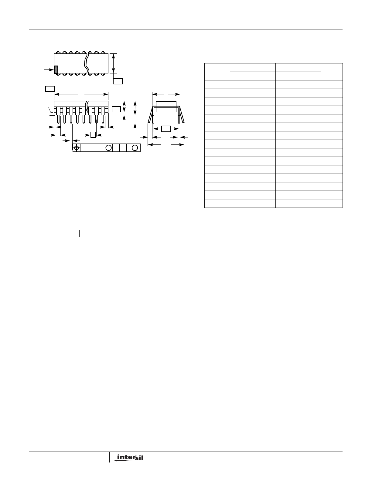
E16.3 (JEDEC MS-001-BB ISSUE D)
16 LEAD DUAL-IN-LINE PLASTIC PACKAGE
INCHES MILLIMETERS
SYMBOL
A-0.210 - 5.33 4
A1 0.015 - 0.39 -4
A2 0.115 0.195 2.93 4.95 -
B 0.014 0.022 0.356 0.558 B1 0.045 0.070 1.15 1.77 8, 10
C 0.008 0.014 0.204 0.355 -
D 0.735 0.775 18.66 19.68 5
D1 0.005 - 0.13 -5
E 0.300 0.325 7.62 8.25 6
E1 0.240 0.280 6.10 7.11 5
e 0.100 BSC 2.54 BSC -
e
A
e
B
0.300 BSC 7.62 BSC 6
- 0.430 - 10.92 7
L 0.115 0.150 2.93 3.81 4
N16 169
NOTESMIN MAX MIN MAX
Rev. 0 12/93
17
FN3142.8
October 30, 2007
Page 18
HI-506, HI-507, HI-508, HI-509
Dual-In-Line Plastic Packages (PDIP)
N
D1
-C-
E1
-B-
A1
A2
E
A
L
e
C
C
L
e
A
C
e
B
INDEX
AREA
BASE
PLANE
SEATING
PLANE
D1
B1
12 3 N/2
-AD
e
B
0.010 (0.25) C AM BS
NOTES:
1. Controlling Dimensions: INCH. In case of conflict between English and
Metric dimensions, the inch dimensions control.
2. Dimensioning and tolerancing per ANSI Y14.5M-1982.
3. Symbols are defined in the “MO Series Symbol List” in Section 2.2 of
Publication No. 95.
4. Dimensions A, A1 and L are measured with the package seated in
JEDEC seating plane gauge GS-3.
5. D, D1, and E1 dimensions do not include mold flash or protrusions.
Mold flash or protrusions shall not exceed 0.010 inch (0.25mm).
6. E and are measured with the leads constrained to be perpendic-
7. e
e
A
ular to datum .
and eC are measured at the lead tips with the leads unconstrained.
B
e
must be zero or greater.
C
-C-
8. B1 maximum dimensions do not include dambar protrusions. Dambar
protrusions shall not exceed 0.010 inch (0.25mm).
9. N is the maximum number of terminal positions.
10. Corner leads (1, N, N/2 and N/2 + 1) for E8.3, E16.3, E18.3, E28.3,
E42.6 will have a B1 dimension of 0.030 - 0.045 inch (0.76 - 1.14mm).
E28.6 (JEDEC MS-011-AB ISSUE B)
28 LEAD DUAL-IN-LINE PLASTIC PACKAGE
INCHES MILLIMETERS
SYMBOL
A-0.250 - 6.35 4
A1 0.015 - 0.39 -4
A2 0.125 0.195 3.18 4.95 -
B 0.014 0.022 0.356 0.558 B1 0.030 0.070 0.77 1.77 8
C 0.008 0.015 0.204 0.381 -
D 1.380 1.565 35.1 39.7 5
D1 0.005 - 0.13 -5
E 0.600 0.625 15.24 15.87 6
E1 0.485 0.580 12.32 14.73 5
e 0.100 BSC 2.54 BSC e
A
e
B
0.600 BSC 15.24 BSC 6
- 0.700 - 17.78 7
L 0.115 0.200 2.93 5.08 4
N28 289
NOTESMIN MAX MIN MAX
Rev. 1 12/00
18
FN3142.8
October 30, 2007
Page 19
HI-506, HI-507, HI-508, HI-509
Ceramic Dual-In-Line Frit Seal Packages (CERDIP)
LEAD FINISH
c1
-A-
-B-
bbb C A - B
S
BASE
PLANE
SEATING
PLANE
S1
b2
b
ccc C A - BMD
D
A
A
e
S
S
NOTES:
1. Index area: A notch or a pin one identification mark shall be located adjacent to pin one and shall be located within the shaded
area shown. The manufacturer’s identification shall not be used
as a pin one identification mark.
2. The maximum limits of lead dimensions b and c or M shall be
measured at the centroid of the finished lead surfaces, when
solder dip or tin plate lead finish is applied.
3. Dimensions b1 and c1 apply to lead base metal only. Dimension
M applies to lead plating and finish thickness.
4. Corner leads (1, N, N/2, and N/2+1) may be configured with a
partial lead paddle. For this configuration dimension b3 replaces
dimension b2.
5. This dimension allows for off-center lid, meniscus, and glass
overrun.
6. Dimension Q shall be measured from the seating plane to the
base plane.
7. Measure dimension S1 at all four corners.
8. N is the maximum number of terminal positions.
9. Dimensioning and tolerancing per ANSI Y14.5M - 1982.
10. Controlling dimension: INCH.
-DBASE
E
D
S
S
Q
A
-CL
METAL
b1
M
(b)
SECTION A-A
α
(c)
M
eA
eA/2
aaa CA - B
M
c
D
S
S
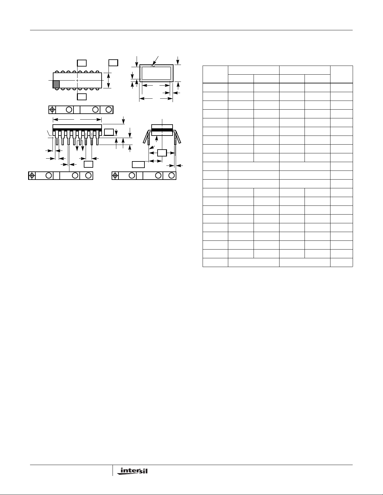
F16.3 MIL-STD-1835 GDIP1-T16 (D-2, CONFIGURATION A)
16 LEAD CERAMIC DUAL-IN-LINE FRIT SEAL PACKAGE
INCHES MILLIMETERS
SYMBOL
A-0.200 - 5.08 -
b 0.014 0.026 0.36 0.66 2
b1 0.014 0.023 0.36 0.58 3
b2 0.045 0.065 1.14 1.65 b3 0.023 0.045 0.58 1.14 4
c 0.008 0.018 0.20 0.46 2
c1 0.008 0.015 0.20 0.38 3
D-0.840 - 21.34 5
E 0.220 0.310 5.59 7.87 5
e 0.100 BSC 2.54 BSC -
eA 0.300 BSC 7.62 BSC -
eA/2 0.150 BSC 3.81 BSC -
L 0.125 0.200 3.18 5.08 -
Q 0.015 0.060 0.38 1.52 6
S1 0.005 - 0.13 -7
o
α
90
105
o
90
o
105
aaa - 0.015 - 0.38 bbb - 0.030 - 0.76 -
ccc - 0.010 - 0.25 -
M-0.0015 - 0.038 2, 3
N16 168
NOTESMIN MAX MIN MAX
o
Rev. 0 4/94
-
19
FN3142.8
October 30, 2007
Page 20
HI-506, HI-507, HI-508, HI-509
Ceramic Dual-In-Line Frit Seal Packages (CERDIP)
LEAD FINISH
c1
-A-
-B-
bbb C A - B
S
BASE
PLANE
SEATING
PLANE
S1
b2
b
ccc C A - BMD
D
A
A
e
S
S
NOTES:
1. Index area: A notch or a pin one identification mark shall be located adjacent to pin one and shall be located within the shaded
area shown. The manufacturer’s identification shall not be used
as a pin one identification mark.
2. The maximum limits of lead dimensions b and c or M shall be
measured at the centroid of the finished lead surfaces, when
solder dip or tin plate lead finish is applied.
3. Dimensions b1 and c1 apply to lead base metal only. Dimension
M applies to lead plating and finish thickness.
4. Corner leads (1, N, N/2, and N/2+1) may be configured with a
partial lead paddle. For this configuration dimension b3 replaces
dimension b2.
5. This dimension allows for off-center lid, meniscus, and glass
overrun.
6. Dimension Q shall be measured from the seating plane to the
base plane.
7. Measure dimension S1 at all four corners.
8. N is the maximum number of terminal positions.
9. Dimensioning and tolerancing per ANSI Y14.5M - 1982.
10. Controlling dimension: INCH.
-DBASE
E
D
S
S
Q
A
-CL
METAL
b1
M
(b)
SECTION A-A
α
(c)
M
eA
eA/2
aaa CA - B
M
c
D
S
S
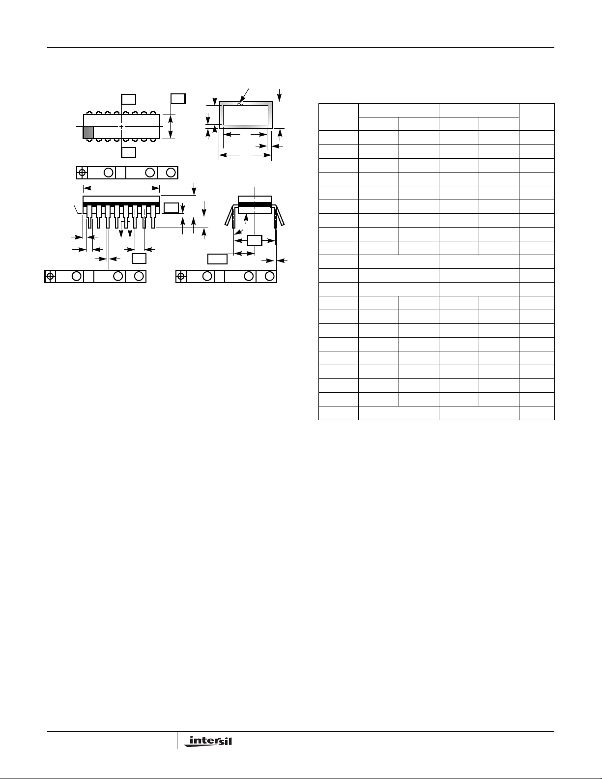
F28.6 MIL-STD-1835 GDIP1-T28 (D-10, CONFIGURATION A)
28 LEAD CERAMIC DUAL-IN-LINE FRIT SEAL PACKAGE
INCHES MILLIMETERS
SYMBOL
A-0.232 - 5.92 -
b 0.014 0.026 0.36 0.66 2
b1 0.014 0.023 0.36 0.58 3
b2 0.045 0.065 1.14 1.65 b3 0.023 0.045 0.58 1.14 4
c 0.008 0.018 0.20 0.46 2
c1 0.008 0.015 0.20 0.38 3
D-1.490 - 37.85 5
E 0.500 0.610 12.70 15.49 5
e 0.100 BSC 2.54 BSC -
eA 0.600 BSC 15.24 BSC -
eA/2 0.300 BSC 7.62 BSC -
L 0.125 0.200 3.18 5.08 -
Q 0.015 0.060 0.38 1.52 6
S1 0.005 - 0.13 -7
o
α
90
105
o
90
o
105
aaa - 0.015 - 0.38 bbb - 0.030 - 0.76 -
ccc - 0.010 - 0.25 -
M-0.0015 - 0.038 2, 3
N28 288
NOTESMIN MAX MIN MAX
o
Rev. 0 4/94
-
20
FN3142.8
October 30, 2007
Page 21
HI-506, HI-507, HI-508, HI-509
Small Outline Plastic Packages (SOIC)
N
INDEX
AREA
123
-A-
E
-B-
SEATING PLANE
D
A
-C-
0.25(0.010) BM M
H
L
h x 45°
α
e
B
0.25(0.010) C AM BS
M
NOTES:
1. Symbols are defined in the “MO Series Symbol List” in Section 2.2 of
Publication Number 95.
2. Dimensioning and tolerancing per ANSI Y14.5M-1982.
3. Dimension “D” does not include mold flash, protrusions or gate burrs.
Mold flash, protrusion and gate burrs shall not exceed 0.15mm (0.006
inch) per side.
4. Dimension “E” does not include interlead flash or protrusions. Interlead
flash and protrusions shall not exceed 0.25mm (0.010 inch) per side.
5. The chamfer on the body is optional. If it is not present, a visual index
feature must be located within the crosshatched area.
6. “L” is the length of terminal for soldering to a substrate.
7. “N” is the number of terminal positions.
8. Terminal numbers are shown for reference only.
9. The lead width “B”, as measured 0.36mm (0.014 inch) or greater above
the seating plane, shall not exceed a maximum value of 0.61mm
(0.024 inch).
10. Controlling dimension: MILLIMETER. Converted inch dimensions are
not necessarily exact.
A1
C
0.10(0.004)
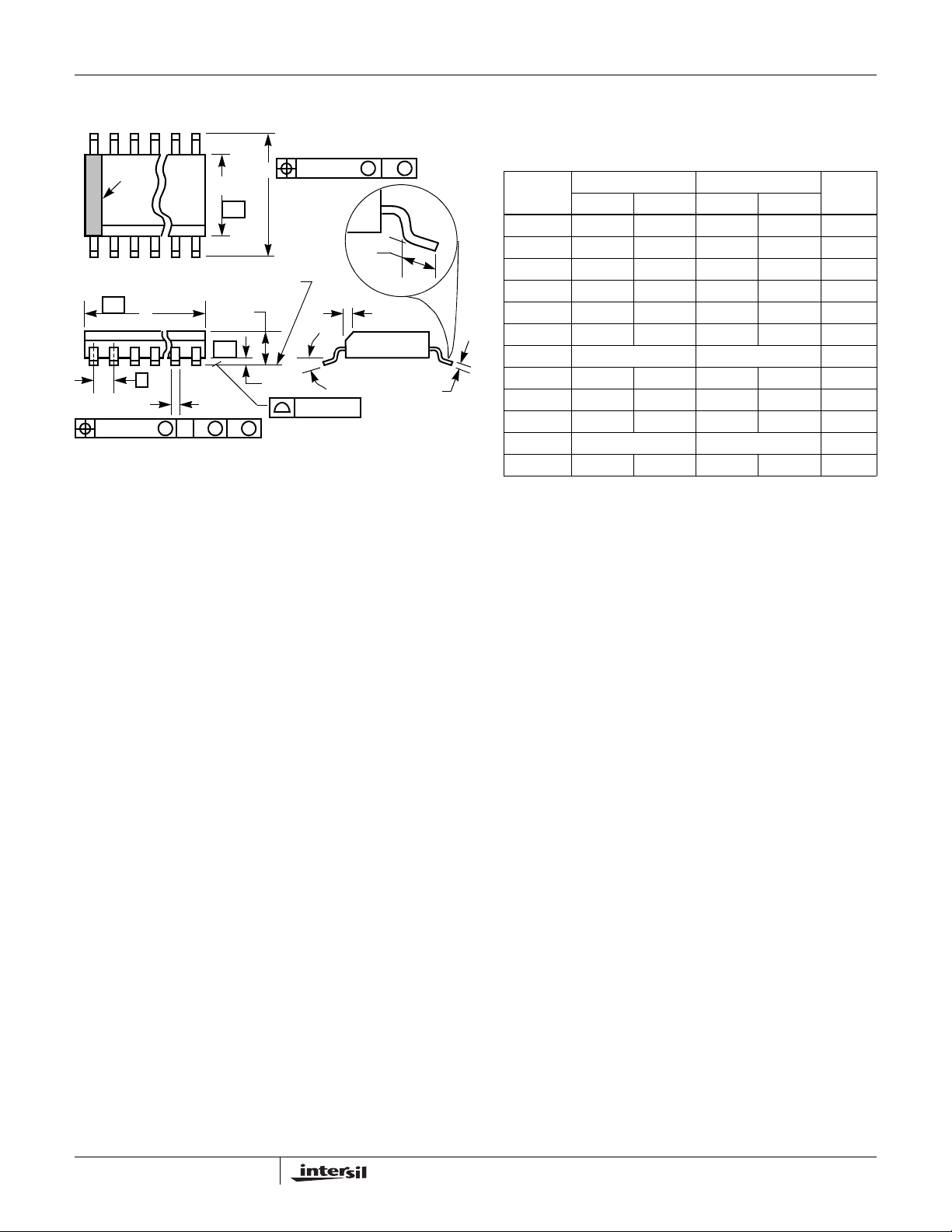
M16.15 (JEDEC MS-012-AC ISSUE C)
16 LEAD NARROW BODY SMALL OUTLINE PLASTIC PACKAGE
INCHES MILLIMETERS
SYMBOL
A 0.0532 0.0688 1.35 1.75 -
A1 0.0040 0.0098 0.10 0.25 -
B 0.013 0.020 0.33 0.51 9
C 0.0075 0.0098 0.19 0.25 D 0.3859 0.3937 9.80 10.00 3
E 0.1497 0.1574 3.80 4.00 4
e 0.050 BSC 1.27 BSC H 0.2284 0.2440 5.80 6.20 h 0.0099 0.0196 0.25 0.50 5
L 0.016 0.050 0.40 1.27 6
N16 167
α
0° 8° 0° 8° -
NOTESMIN MAX MIN MAX
Rev. 1 6/05
21
FN3142.8
October 30, 2007
Page 22
HI-506, HI-507, HI-508, HI-509
Small Outline Plastic Packages (SOIC)
N
INDEX
AREA
123
-A-
E
-B-
SEATING PLANE
D
A
-C-
0.25(0.010) BM M
H
L
h x 45
o
α
e
B
0.25(0.010) C AM BS
M
NOTES:
1. Symbols are defined in the “MO Series Symbol List” in Section 2.2
of Publication Number 95.
2. Dimensioning and tolerancing per ANSI Y14.5M-1982.
3. Dimension “D” does not include mold flash, protrusions or gate
burrs. Mold flash, protrusion and gate burrs shall not exceed
0.15mm (0.006 inch) per side.
4. Dimension “E” does not include interlead flash or protrusions. Interlead flash and protrusions shall not exceed 0.25mm (0.010
inch) per side.
5. The chamfer on the body is optional. If it is not present, a visual
index feature must be located within the crosshatched area.
6. “L” is the length of terminal for soldering to a substrate.
7. “N” is the number of terminal positions.
8. Terminal numbers are shown for reference only.
9. The lead width “B”, as measured 0.36mm (0.014 inch) or greater
above the seating plane, shall not exceed a maximum value of
0.61mm (0.024 inch)
10. Controlling dimension: MILLIMETER. Converted inch dimensions are not necessarily exact.
A1
0.10(0.004)
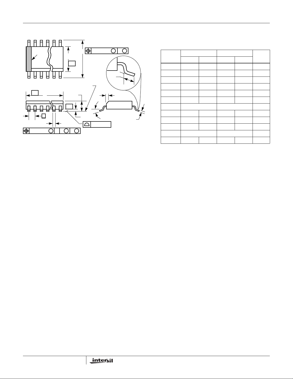
M28.3 (JEDEC MS-013-AE ISSUE C)
28 LEAD WIDE BODY SMALL OUTLINE PLASTIC PACKAGE
INCHES MILLIMETERS
SYMBOL
A 0.0926 0.1043 2.35 2.65 -
A1 0.0040 0.0118 0.10 0.30 -
B 0.013 0.0200 0.33 0.51 9
C 0.0091 0.0125 0.23 0.32 -
D 0.6969 0.7125 17.70 18.10 3
E 0.2914 0.2992 7.40 7.60 4
e 0.05 BSC 1.27 BSC -
H 0.394 0.419 10.00 10.65 -
C
h 0.01 0.029 0.25 0.75 5
L 0.016 0.050 0.40 1.27 6
N28 287
o
α
0
o
8
o
0
o
8
Rev. 0 12/93
NOTESMIN MAX MIN MAX
-
22
FN3142.8
October 30, 2007
Page 23
HI-506, HI-507, HI-508, HI-509
Plastic Leaded Chip Carrier Packages (PLCC)
0.042 (1.07)
0.048 (1.22)
PIN (1) IDENTIFIER
0.020 (0.51) MAX
3 PLCS
C
L
D1
D
0.026 (0.66)
0.032 (0.81)
0.045 (1.14)
MIN
0.042 (1.07)
0.056 (1.42)
0.050 (1.27) TP
VIEW “A” TYP.
C
L
EE1
0.013 (0.33)
0.021 (0.53)
0.025 (0.64)
MIN
0.004 (0.10) C
0.025 (0.64)
0.045 (1.14)
D2/E2
D2/E2
A1
A
-C-
R
VIEW “A”
0.020 (0.51)
MIN
SEATING
PLANE
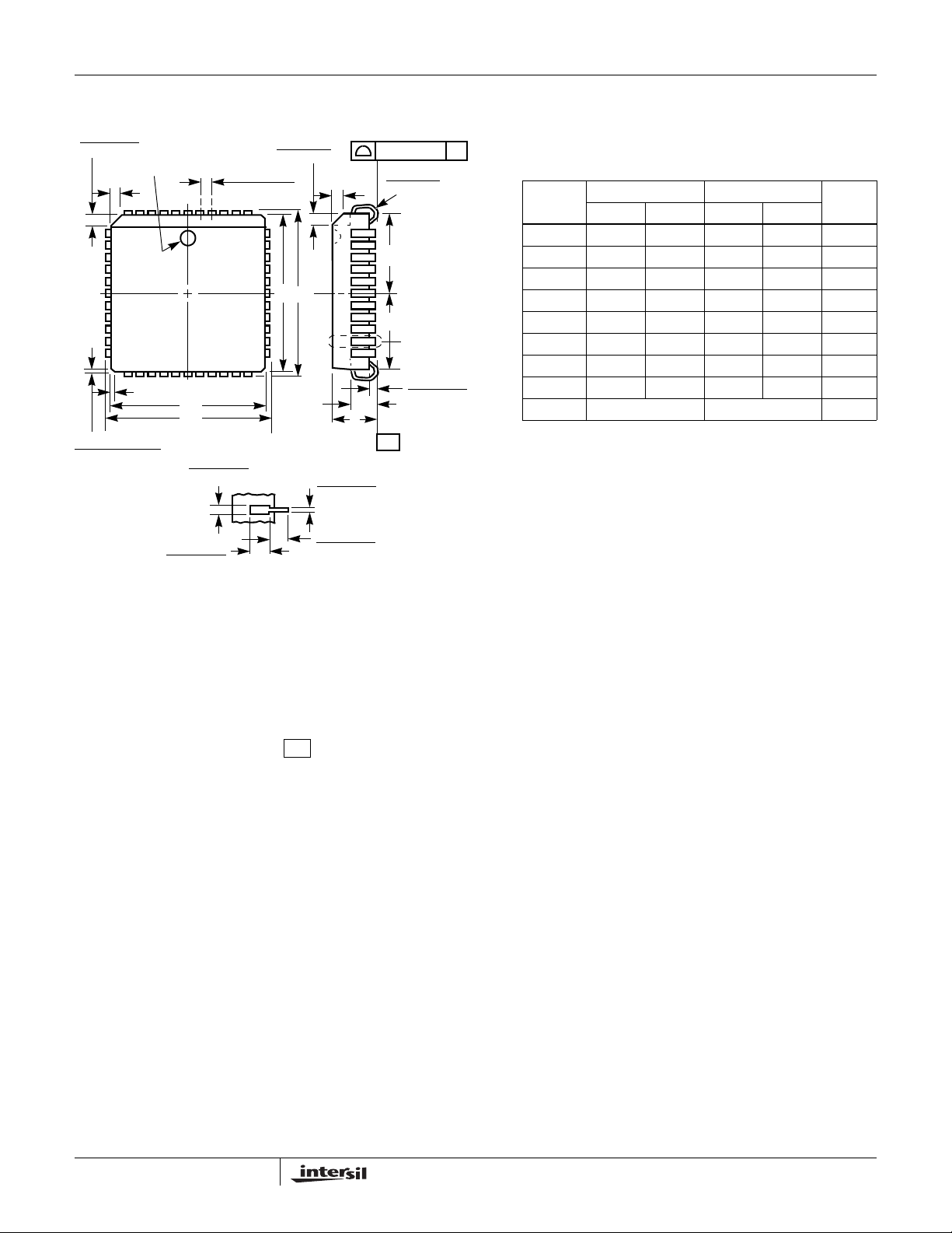
N20.35 (JEDEC MS-018AA ISSUE A)
20 LEAD PLASTIC LEADED CHIP CARRIER PACKAGE
INCHES MILLIMETERS
SYMBOL
A 0.165 0.180 4.20 4.57 -
A1 0.090 0.120 2.29 3.04 -
D 0.385 0.395 9.78 10.03 D1 0.350 0.356 8.89 9.04 3
D2 0.141 0.169 3.59 4.29 4, 5
E 0.385 0.395 9.78 10.03 E1 0.350 0.356 8.89 9.04 3
E2 0.141 0.169 3.59 4.29 4, 5
N20 206
NOTESMIN MAX MIN MAX
Rev. 2 11/97
NOTES:
1. Controlling dimension: INCH. Converted millimeter dimensions are
not necessarily exact.
2. Dimensions and tolerancing per ANSI Y14.5M-1982.
3. Dimensions D1 and E1 do not include mold protrusions. Allowable
mold protrusion is 0.010 inch (0.25mm) per side. Dimensions D1
and E1 include mold mismatch and are measured at the extreme
material condition at the body parting line.
4. To be measured at seating plane contact point.
-C-
5. Centerline to be determined where center leads exit plastic body.
6. “N” is the number of terminal positions.
23
FN3142.8
October 30, 2007
Page 24
HI-506, HI-507, HI-508, HI-509
Plastic Leaded Chip Carrier Packages (PLCC)
0.042 (1.07)
0.048 (1.22)
PIN (1) IDENTIFIER
0.020 (0.51) MAX
3 PLCS
C
L
D1
D
0.026 (0.66)
0.032 (0.81)
0.045 (1.14)
MIN
0.050 (1.27) TP
0.042 (1.07)
0.056 (1.42)
EE1
VIEW “A” TYP.
C
L
A
0.013 (0.33)
0.021 (0.53)
0.025 (0.64)
MIN
0.004 (0.10) C
0.025 (0.64)
0.045 (1.14)
D2/E2
D2/E2
A1
-C-
VIEW “A”
0.020 (0.51)
MIN
SEATING
PLANE
NOTES:
1. Controlling dimension: INCH. Converted millimeter dimensions are
not necessarily exact.
2. Dimensions and tolerancing per ANSI Y14.5M-1982.
3. Dimensions D1 and E1 do not include mold protrusions. Allowable
mold protrusion is 0.010 inch (0.25mm) per side. Dimensions D1
and E1 include mold mismatch and are measured at the extreme
material condition at the body parting line.
4. To be measured at seating plane contact point.
-C-
5. Centerline to be determined where center leads exit plastic body.
6. “N” is the number of terminal positions.
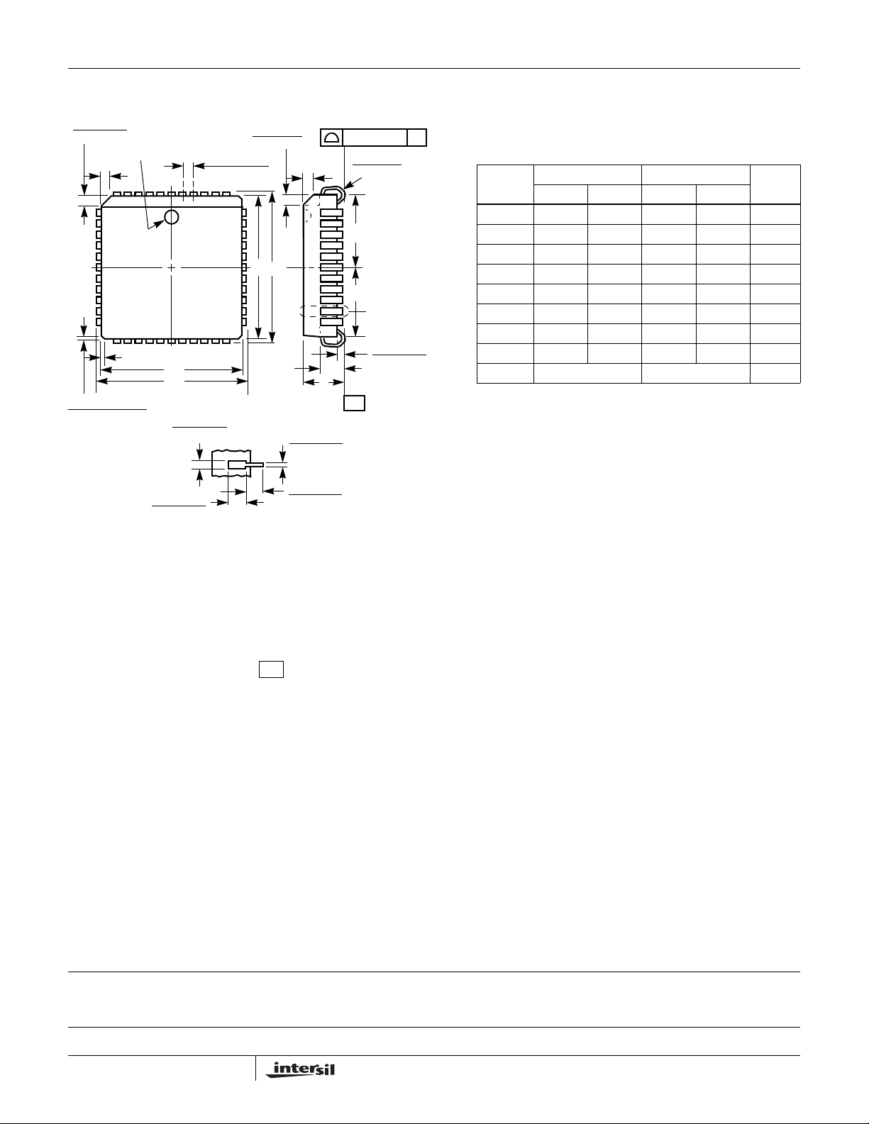
N28.45 (JEDEC MS-018AB ISSUE A)
R
28 LEAD PLASTIC LEADED CHIP CARRIER PACKAGE
INCHES MILLIMETERS
SYMBOL
NOTESMIN MAX MIN MAX
A 0.165 0.180 4.20 4.57 -
A1 0.090 0.120 2.29 3.04 -
D 0.485 0.495 12.32 12.57 D1 0.450 0.456 11.43 11.58 3
D2 0.191 0.219 4.86 5.56 4, 5
E 0.485 0.495 12.32 12.57 -
E1 0.450 0.456 11.43 11.58 3
E2 0.191 0.219 4.86 5.56 4, 5
N28 286
Rev. 2 11/97
All Intersil U.S. products are manufactured, assembled and tested utilizing ISO9000 quality systems.
Intersil Corporation’s quality certifications can be viewed at www.intersil.com/design/quality
Intersil products are sold by description only. Intersil Corporation reserves the right to make changes in circuit design, software and/or specifications at any time without
notice. Accordingly, the reader is cautioned to verify that data sheets are current before placing orders. Information furnished by Intersil is believed to be accurate and
reliable. However, no responsibility is assumed by Intersil or its subsidiaries for its use; nor for any infringements of patents or other rights of third parties which may result
from its use. No license is granted by implicat ion or oth erwise u nde r any p a tent or p at ent r ights of Intersil or its subsidiari es.
For information regarding Intersil Corporation and its products, see www.intersil.com
24
FN3142.8
October 30, 2007
 Loading...