

August 1997
HI2315
10-Bit, 80 MSPS D/A Converter
(Ultra-Low Glitch Version)
Features
• Throughput Rate . . . . . . . . . . . . . . . . . . . . . . . . . 80MHz
• Low Power . . . . . . . . . . . . . . . . . . . . . . . . . . . . . .150mW
• Single Power Supply . . . . . . . . . . . . . . . . . . . . . . . . .+5V
• Differential Linearity Error . . . . . . . . . . . . . . . ±0.5 LSB
• TTL/CMOS Compatible Inputs
• Built in Bandgap Voltage Reference
• Power Down and Blanking Control Pins
• Low Glitch
• Pin Compatible with Sony CXD2306
• Direct Replacement for Sony CXD2315Q
Applications
• Wireless Communications
• Direct Digital Frequency Synthesis
• Signal Reconstruction
• Test Equipment
• High Resolution Imaging and Graphics Systems
Description
The HI2315 is a 10-bit, 80MHz, high speed, low power CMOS
D/A converter. The converter incor porates a 10-bit input data
register with current outputs. The HI2315 includes a power
down feature that reduces power consumption and a blanking
control. The on-chip bandgap reference can be used to set the
output current range of the D/A.
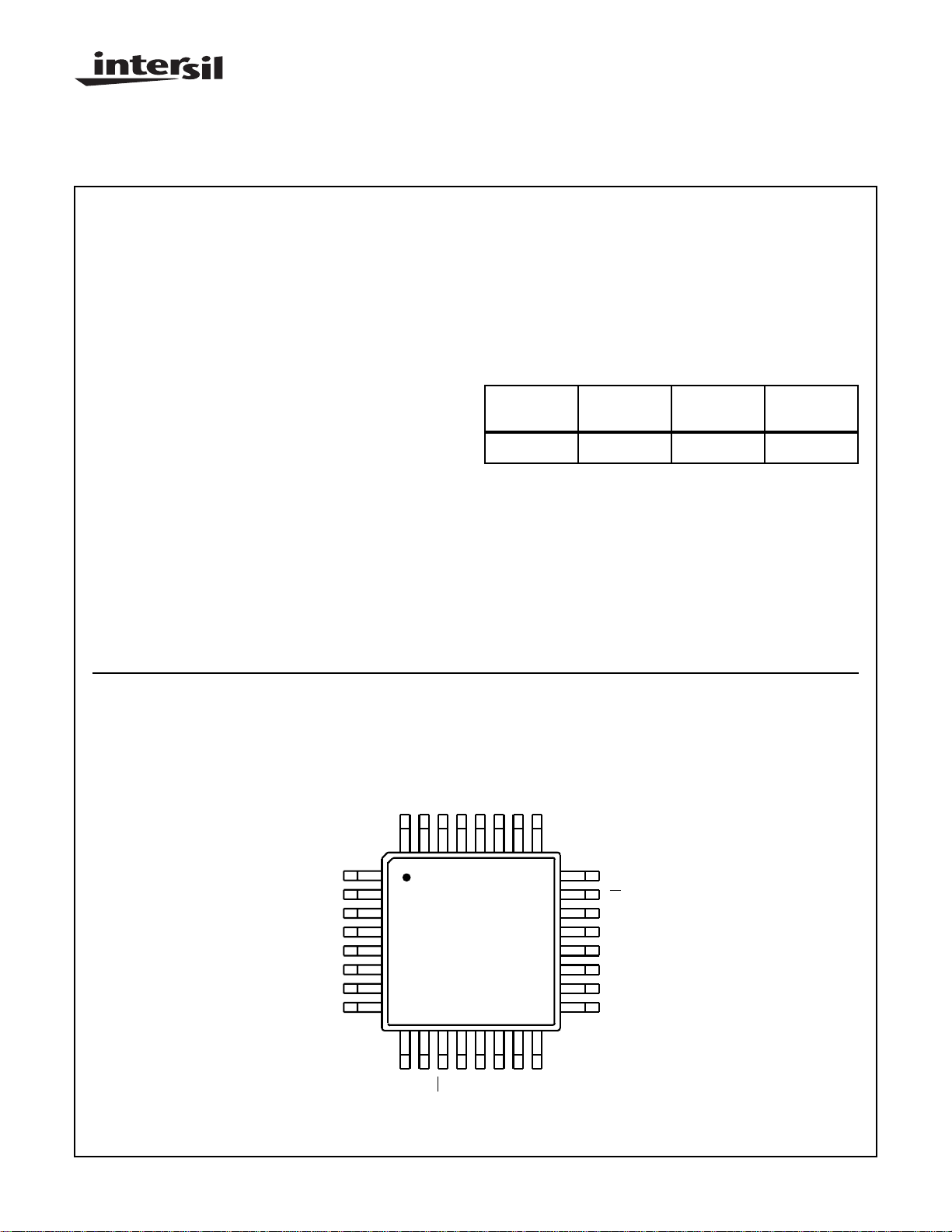
Ordering Information
PART
NUMBER
HI2315JCQ -20 to 75 32 Ld MQFP Q32.7x7-S
TEMP.
RANGE (oC) PACKAGE PKG. NO.
Pinout
D3
D4
D5
D6
D7
D8
D9 (MSB)
NC
HI2315
(MQFP)
TOP VIEW
SS
DD
NC
D0 (LSB)
D1
D2
32 31 30 29 28 27 26 25
1
2
3
4
5
6
7
8
9 10111213141516
CE
BLK
CLK
NC
DV
DV
DD
DV
VB
NC
DV
SS
AV
24
23
22
21
20
19
18
17
NC
SS
IO
IO
VG
AV
AV
V
S
I
REF
DD
DD
REF
REF
CAUTION: These devices are sensitive to electrostatic discharge; follow proper IC Handling Procedures.
http://www.intersil.com or 407-727-9207
| Copyright © Intersil Corporation 1999
10-1
File Number 4119.1
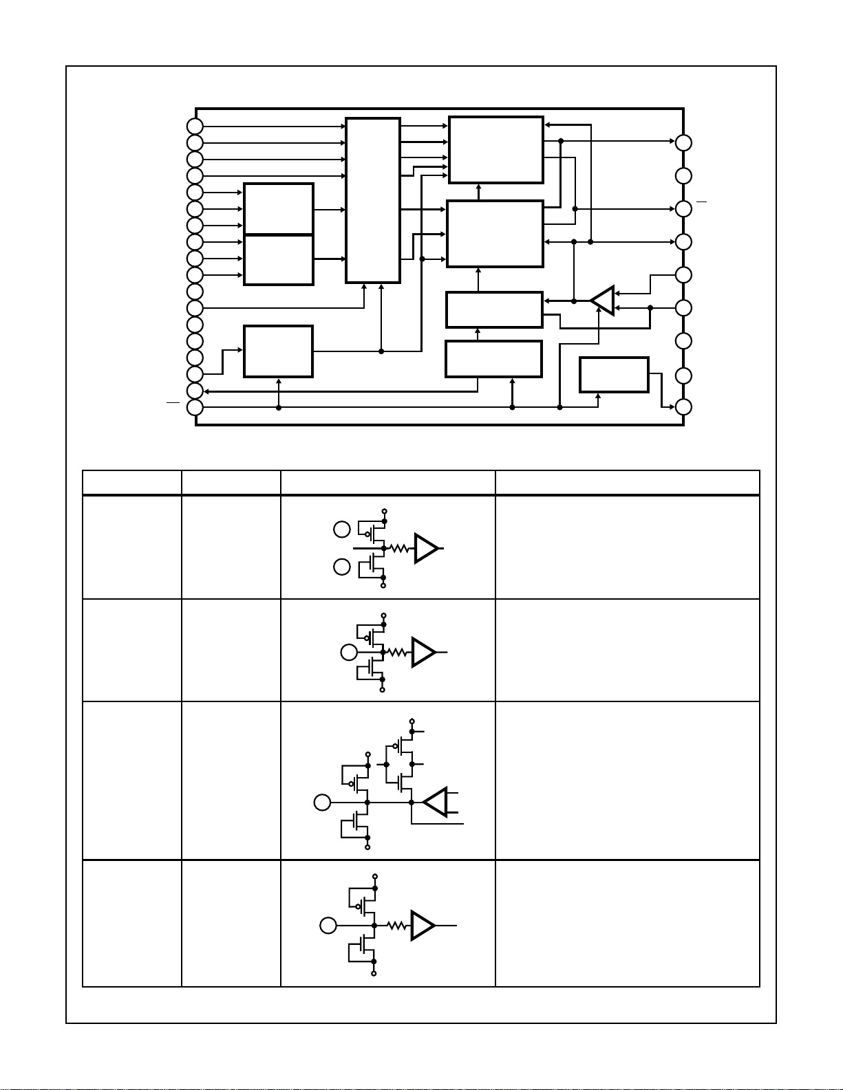
Functional Block Diagram
HI2315
DV
DV
DV
DV
D1
D2
D3
D4
D5
D6
D7
D8
D9
DD
BLK
DD
SS
SS
CLK
VB
CE
30
31
32
1
2
3
4
5
6
7
28
10
13
15
27
9
14
11
DECODER
DECODER
CLOCK
GENERATOR
LATCHES
4 LSBs
CURRENT
CELLS
6 MSBs
CURRENT
CELLS
CURRENT CELLS
(FOR FULL SCALE)
BIAS VOLTAGE
GENERATOR
BAND GAP
REFERENCE
(LSB) D0
Pin Descriptions
PIN NO. SYMBOL EQUIVALENT CIRCUIT DESCRIPTION
30 to 32
1 to 7
D0 to D9 Digital Input.
30
TO
7
DV
DV
DD
SS
IO
24
AV
25
SS
IO
23
22
VG
19
V
REF
-
+
17
I
REF
21
AV
DD
20
AV
DD
18
S
REF
10 BLK Blanking pin. No signal (0V output) at high and
10
14 VB Connect a capacitor of approximately 0.1µF.
14
9 CLK Clock pin.
9
DV
DD
DV
DV
DV
SS
DV
DV
DD
SS
DD
SS
DV
DD
output state at low.
+
-
10-2
HI2315
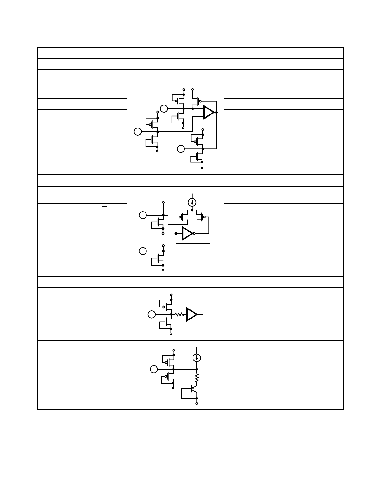
Pin Descriptions
(Continued)
PIN NO. SYMBOL EQUIVALENT CIRCUIT DESCRIPTION
15, 27 DV
25 AV
17 I
19 V
22 VG Connect a capacitor of approximately 0.1µF.
20, 21 AV
REF
REF
SS
SS
DD
AV
DD
17
AV
DD
AV
19
AV
SS
SS
AV
DD
+
-
AV
22
AV
SS
Digital GND.
Analog GND.
Connect resistance “16R” which is 16 times output
resistance “R”.
Sets output full scale value.
DD
Analog VDD.
24 IO Current Output pin. Output can be retrieved by
AV
DD
connecting resistance. The standard is 200Ω.
23 IO Inverted Current Output pin. Connect to GND
24
normally.
AV
SS
AV
DD
23
AV
SS
13, 28 DV
11 CE Chip Enable pin. No signal (0V output) at high makes
18 S
DD
REF
DV
DD
11
DV
SS
AV
DD
Digital VDD.
power consumption minimum.
Independent Constant-Voltage Source Output pin
using band gap reference. Stable voltage
independent of the fluctuation for supply voltage can
18
AV
SS
be obtained by connecting to V
Circuit 2 for details.
. See Application
REF
10-3

HI2315
Absolute Maximum Ratings T
Supply Voltage (VDD). . . . . . . . . . . . . . . . . . . . . . . . . . . . . . . . . . 7V
Input Voltage (VIN) . . . . . . . . . . . . . . . . . . .VSS -0.5V to VDD + 0.5V
Output Voltage (I
). . . . . . . . . . . . . . . . . . . . . . . . . .0mA to 15mA
OUT
Operating Conditions
Supply Voltage
=25oC Thermal Information
A
Thermal Resistance (Typical, Note 1) θJA (oC/W)
MQFP Package. . . . . . . . . . . . . . . . . . . . . . . . . . . . 122
Maximum Junction Temperature (MQFP Package) . . . . . . . . 150oC
Maximum Storage Temperature Range . . . . . . . . . .-65oC to 150oC
Maximum Lead Temperature (Soldering 10s). . . . . . . . . . . . . 300oC
(MQFP - Lead Tips Only)
AVDD, AVSS . . . . . . . . . . . . . . . . . . . . . . . . . . . . . . . 5.0V ±0.25V
DVDD, DVSS. . . . . . . . . . . . . . . . . . . . . . . . . . . . . . . .5.0V ±0.25V
Reference Input Voltage (V
Clock Pulse Width (t
Temperature Range (T
CAUTION: Stresses above those listed in “Absolute Maximum Ratings” may cause permanent damage to the device. This is a stress only rating and operation
of the device at these or any other conditions above those indicated in the operational sections of this specification is not implied.
PW1
OPR
). . . . . . . . . . . . . . . . . . .0.5V to 2.0V
REF
, t
). . . . . . . . . . . . . . . . . . 6.25ns (Min)
PW0
) . . . . . . . . . . . . . . . . . . . . -20oC to 75oC
NOTE:
1. θJA is measured with the component mounted on an evaluation PC board in free air.
Electrical Specifications T
= 25oC, f
A
= 80MHz, VDD = 5V, R = 200Ω, V
CLK
= 2.0V, 16R = 3.3kΩ
REF
PARAMETER SYMBOL TEST CONDITIONS MIN TYP MAX UNITS
Resolution n - 10 - Bit
Maximum Conversion Rate f
MAX
80 - - MHz
Linearity Error EL -1.5 - 1.5 LSB
Differential Linearity Error ED -0.5 - 0.5 LSB
Output Full-Scale Voltage V
Output Full-Scale Current I
Output Off-Set Voltage V
FS
FS
OS
1.8 1.94 2.0 V
9.0 9.7 10 mA
-- 1mV
Output Impedance - 300 - kΩ
Supply Current I
Digital Input Current High Level I
Low Level I
Digital Input Voltage High Level V
Low Level V
Accuracy Guarantee Output Voltage Range V
Setup Time t
Hold Time t
Rise Time t
Propagation Delay Time t
DD
IH
IL
IH
IL
OC
S
H
r
PD
Glitch Energy GE R
= 200Ω, 2V
OUT
P-P
- - 30 mA
-- 5µA
-5 - - µA
2.45 - - V
- - 0.85 V
1.8 1.94 2.0 V
3.0 - - ns
3.0 - - ns
5.0 - - ns
-5 - ns
- - 30 pV/s
Differential Gain DG - - 1.0 %
Differential Phase DP - - 1.0 Degrees
S
Output Voltage S
REF
REF
TA = 25oC 1.0 1.2 1.4 V
10-4

Test Circuits
10-BIT
COUNTER
WITH
LATCH
30
31
7
HI2315
D0 (LSB)
D9 (MSB)
VG
23
IO
0.1µ
22
AV
DD
OSCILLOSCOPE
200
80MHz (MAX)
SQUARE
CLK
10MHz (MAX)
SQUARE
WAVE
CLK
WAVE
CONTROLLER
SQUARE
FREQUENCY
DEMULTIPLIER
CLK
80MHz
WAVE
2V
3.3K
5K
AV
SS
0.1µ
9
CLK
BLK
10
11
CE
14
VB
19
V
REF
17
I
REF
FIGURE 1. MAXIMUM CONVERSION RATE TEST CIRCUIT
30
0.1µ
31
7
9
10
11
14
D0 (LSB)
D9 (MSB)
CLK
BLK
CE
VB
V
REF
I
REF
VG
23
IO
0.1µ
22
19
17
2V
3.3K
AV
5K
AV
FIGURE 2. DC CHARACTERISTICS TEST CIRCUIT
30
0.1µ
31
7
9
10
11
14
D0 (LSB)
D9 (MSB)
CLK
BLK
CE
VB
V
REF
I
REF
VG
23
IO
0.1µ
22
19
17
2V
3.3K
AV
5K
AV
DD
SS
DD
SS
DVM
200
OSCILLOSCOPE
200
CLK
1MHz
SQUARE
WAVE
FIGURE 3. PROPAGATION DELAY TIME TEST CIRCUIT
30
31
7
9
10
11
14
D0 (LSB)
D9 (MSB)
CLK
BLK
CE
VB
23
IO
0.1µ
22
VG
2V
19
V
REF
17
I
REF
3.3K
10-BIT
COUNTER
WITH
LATCH
DELAY
CONTROLLER
DELAY
CONTROLLER
0.1µ
FIGURE 4. SETUP HOLD TIME AND GLITCH ENERGY TEST CIRCUIT
10-5
5K
AV
AV
DD
SS
200
OSCILLOSCOPE

Timing Diagram
HI2315
t
t
PW1
PW0
CLK
t
t
S
H
t
PD
DAT A
D/A OUT
tSt
H
t
PD
Typical Application Circuits
25
26
27
28
C
29
t
t
S
H
t
PD
IO IO VG
AV
SS
NC
DV
SS
DV
DD
NC
R1
C
100%
50%
0%
C
AVDDAV
TABLE 1. I/O CORRESPONDENCE TABLE
(2.00V Output Full Scale Voltage)
INPUT CODE OUTPUT VOLTAGE
MSB LSB
1111111111 2.0V
•
•
•
1000000000 1.0V
•
•
•
0000000000 0V
AV
AV
DD
SS
DD
R3
R4
R2
1718192021222324
S
V
REF
REF
DV
DV
I
REF
NC
SS
VB
DD
NC
16
15
14
C
13
12
DV
DV
DD
SS
30
D0
31
D1
32
D2
D3
D4
D5
D6
D8 D9 NC
D7
CE
BLK
CLK
87654321
11
10
9
CLOCK INPUT
NOTE:
2. When 5.0V supply voltage (DVDD and AVDD). Digital input from pins 30 to 32 and pins 1 to 7. Pin 18 is Left Open When Using Normally.
R1 = 200Ω, R2 = 3.3Ω (Resistance 16 Times R1), R3 = 3.0kΩ, R4 = 2.0kΩ, C = 0.1µF.
FIGURE 5. APPLICATION CIRCUIT 1
10-6

HI2315
Typical Application Circuits
C
(Continued)
IO IO VG
25
AV
SS
26
NC
27
DV
SS
28
DV
DD
29
NC
30
D0
D1
31
D2
32
D3
R1
D4
C
AVDDAV
D5
D6
C
V
REF
DD
D8 D9 NC
D7
S
REF
DV
DV
1718192021222324
I
REF
BLK
CLK
87654321
NC
SS
VB
DD
NC
CE
R2
16
15
14
13
12
11
10
9
AV
DD
AV
SS
C
CLOCK INPUT
DV
DV
DD
SS
NOTE:
3. When 5.0V supply voltage (DVDD and AVDD). Digital input from pins 30 to 32 and pins 1 to 7. R1 = 200Ω, R2 = 2.0kΩ, C = 0.1µF.
FIGURE 6. APPLICATION CIRCUIT 2
Typical Performance Curves
2.0
1.0
OUTPUT FULL SCALE VOLTAGE (V)
REFERENCE VOLTAGE (V)
FIGURE 7. OUTPUT FULL SCALE VOL TAGE (VFS) vs
REFERENCE VOLTAGE (V
REF
)
∆V = 0.2mV/oC
1.95
1.93
OUTPUT FULL SCALE VOLTAGE (V)
0
2.01.0
-250 255075
AMBIENT TEMPERATURE (
o
C)
FIGURE 8. OUTPUT FULL SCALE VOL TAGE vs AMBIENT
TEMPERA TURE
10-7

HI2315
Typical Performance Curves
∆V = 0.7mV/oC
1.25
1.15
OUTPUT VOLTAGE (V)
REF
S
0
-250 255075
AMBIENT TEMPERATURE (
FIGURE 9. S
vs AMBIENT TEMPERATURE FIGURE 10. OUTPUT FREQUENCY vs CURRENT CONSUMPTION
REF
(Continued)
o
C)
30
20
CURRENT CONSUMPTION (mA)
0
110203040
OUTPUT FREQUENCY (MHz)
NOTE:
4. Standard Measurement Conditions and Description: VDD = 5.0V, V
= 2.0V, R = 200Ω, 16R - 3.3kΩ, TA = 25oC. The temperature
REF
characteristics of external input data in Figure 10 = all “0” and “1” of rectangular wave; clock frequency = 80MHz.
GE (Glitch Energy)
GE, as described in the HI2315, is a spike noise which
appears synchronizing with the clock falling edge when the
input data (for 1 to 1024 input) changes to 128, 256, 384,
512, 640, 768, 896, and 1024. Figure 11 shows the change
state of GE for the staircase wave output, and Figure 12
shows the repetitive output waveform where the GE
appears. These figures exhibit the difference of this IC from
the convention device.
The HI2315 reduces the GE as shown in Figures 11 and 12.
2.0
1.0
ANALOG OUTPUT (V)
0
DIGITAL INPUT (V)
FIGURE 11. CHANGE OF GE FOR STAIRCASE WAVE OUTPUT
512 1024
CONVENTIONAL
DEVICE
HI2315
CLK
10-8

HI2315
HI5780 (GE TYP = 200pV/S)
HI2315 (GE TYP = 10pV/S)
FIGURE 12. REPETITIVE OUTPUT WAVEFORM WHERE GE APPEARS (FOR 200Ω, 2V
Notes On Operation
• Selecting the Output Resistance
- HI2315 is a current output type D/A converter. To create
the output voltage, connect the resistor to the current
output pin.
Specifications:
Output full-scale voltage VFS (Max) = 2.0V
Output full-scale current I
- Calculate the output resistance from V
Connect a resistance sixteen times the output
resistance to the reference current pin I
cases, as this value may not exist, a similar value can
be used instead.
Note that the V
= V
V
FS
REF
will be the following:
FS
x 16 R/R’.
- R is the resistor to be connected to the IO and R’ is the
resistor to be connected to the I
tion can be reduced by increasing the resistance, but
this will on the contrary increase the glitch energy and
data settling time. Set the best values according to the
purpose of use.
• Correlation between Data and Clock
- For the HI2315 to display the desired performance as a
D/A converter, the data transmitted f orm outside and the
clock must be synchronized properly. Adjust the setup
time (t
) and hold time (tH) as specified in “Electrical
S
Characteristics.”
(Max) = 10mA
FS
REF
= IFS x R.
FS
. In some
REF
. Power consump-
OUTPUT)
P-P
• Latch up
- The AV
and DVDD pins must be able to share the
DD
same power supply of the board. This is prevent latch
up caused by potential difference between the two pins
when the power is turned on.
•I
pin
REF
- The I
pin is very sensitive to improve the AC
REF
characteristics. Pay attention for capacitance
component not to attach to this pin because its output
may become unstable.
• VG Pin
- It is recommended to use a 1µF capacitor to improve
the AC characteristics though the typical capacitance
value externally connected to the VG pin is 0.1µF.
•S
REF
- The S
connecting it to the V
is independent regulated current source. By
REF
, stable output amplitudes that
REF
do not depend on fluctuations in the power supply can
be obtained.
- In this case, as V
FS
= S
x 16R/R’, set the V
REF
according to R’.
- Do not use this pin as a reference power supply for
other ICs because this is dedicated for the D/A
converter.
FS
•V
, V
DD
SS
- Separate the analog and digital signals around the
device to reduce noise effects. By-pass the V
DD
pin to
each GND with a 0.1µF ceramics capacitor as near to
the pin as possible for both the digital and analog
signals.
All Intersil semiconductor products are manufactured, assembled and tested under ISO9000 quality systems certification.
Intersil products are sold by description only. Intersil Corporation reserves the right to make changes in circuit design and/or specifications at any time without
notice. Accordingly, the reader is cautioned to verify that data sheets are current before placing orders. Information furnished by Intersil is believed to be accurate
and reliable. However, no responsibility is assumed by Intersil or its subsidiaries for its use; nor f or any infringements of patents or other rights of third parties which
may result from its use. No license is granted by implication or otherwise under an y patent or patent rights of Intersil or its subsidiaries.
For information regarding Intersil Corporation and its products, see web site http://www.intersil.com
10-9
 Loading...