

August 1997
Semiconductor
See HI1178
NOT RECOMMENDED FOR NEW DESIGNS
HI2304
Triple 8-Bit, 20 MSPS, RGB,
3-Channel D/A Converter
Features
• Resolution . . . . . . . . . . . . . . . . . . . . . . . . . . .Triple 8-Bit
• Maximum Conversion Speed . . . . . . . . . . . . . . . 20MHz
• RGB 3-Channel Input/Output
• Differential Linearity Error . . . . . . . . . . . . . . . ±0.5 LSB
• Low Power Consumption . . . . . . . . . . . . . . . . . . .50mW
(330Ω Load for 1.2V
P-P
Output)
• Single Power Supply . . . . . . . . . . . . . . . . . . . . . . . +3.3V
• Low Glitch Noise
• Direct Replacement for Sony CXD2304
Applications
• Digital TV
• Graphics Display
• High Resolution Color Graphics
• Video Reconstruction
• Instrumentation
• Image Processing
• I/Q Modulation
Description
The HI2304 is a triple 8-bit, high-speed, CMOS D/A
converter designed for video band use. It has three
separate, 8-bit, pixel inputs, one each for red, green, and
blue video data. A single 3.3V power supply and pixel clock
input can be controlled individually, or connected together
as one. The HI2304 also has BLANK video control signal.
For faster speed and 5.0V operation, refer to the HI1178.
Ordering Information
PART
NUMBER
HI2304JCQ -20 to 75 48 Ld MQFP Q48.7x7-S
TEMP.
RANGE (oC) PACKAGE PKG. NO.
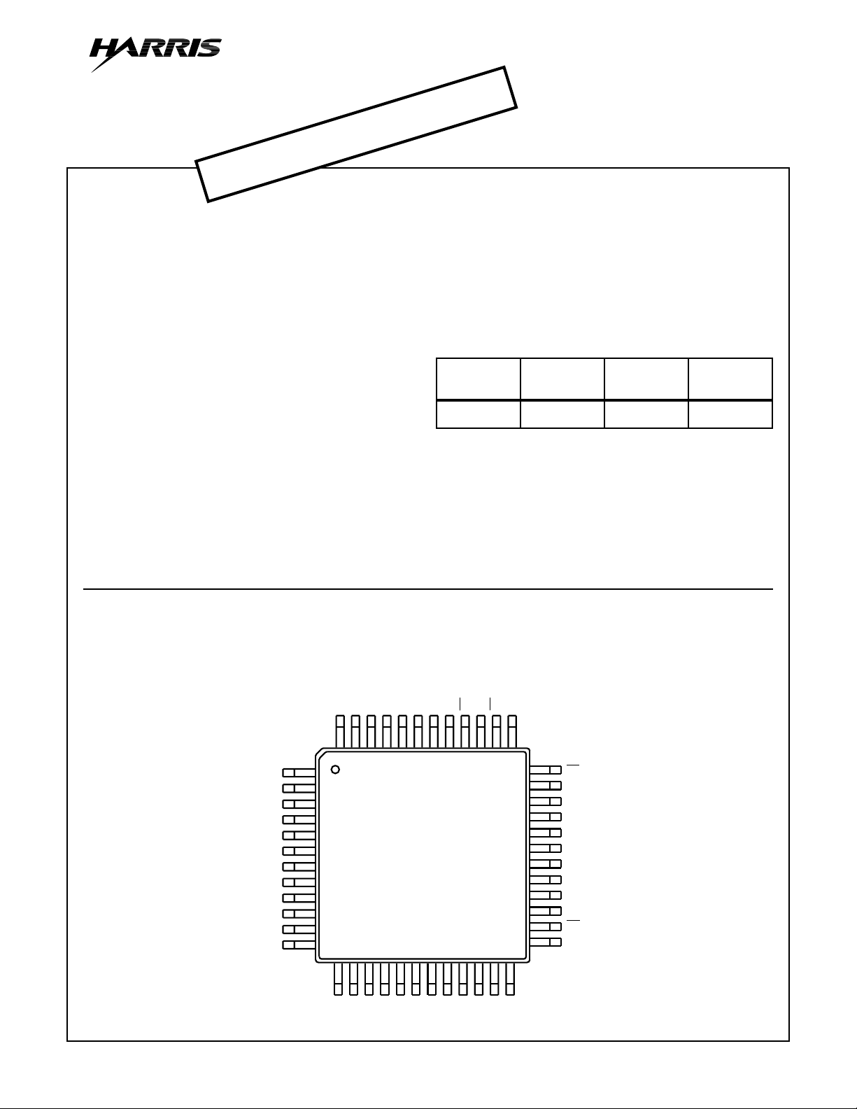
Pinout
R0
R1
R2
R3
R4
R5
R6
R7
G0
G1
G2
G3
DD
DVDDAV
DV
1
2
3
4
5
6
7
8
9
10
11
12
13 14 15 16
G5
G4
G6
DD
G7
HI2304
(MQFP)
TOP VIEW
DD
DD
AV
AVDDAV
B1
B0
VG
B2
B3
B0
B4
B0
B5
G0
G0
B6
R0
373839404142434445464748
36
35
34
33
32
31
30
29
28
27
26
25
2423222120191817
B7
R0
I
REF
V
REF
AV
VB
DV
DV
BCK
GCK
RCK
CE
BLK
SS
SS
SS
CAUTION: These devices are sensitive to electrostatic discharge. Users should follow proper IC Handling Procedures.
Copyright
© Harris Corporation 1997
10-1
File Number 4116.1
Functional Block Diagram
HI2304
(LSB) R0
R1
R2
R3
R4
R5
R6
R7
(LSB) G0
G1
G2
G3
G4
G5
G6
G7
(LSB) B0
B1
B2
B3
B4
B5
B6
B7
BLK
1
2
3
4
5
6
7
8
9
10
11
12
13
14
15
16
17
18
19
20
21
22
23
24
25
DECODER
DECODER
DECODER
DECODER
DECODER
DECODER
LATCHES
LATCHES
LATCHES
2 LSBs
CURRENT
CELLS
6 MSBs
CURRENT
CELLS
CLOCK
GENERATOR
2 LSBs
CURRENT
CELLS
6 MSBs
CURRENT
CELLS
CLOCK
GENERATOR
2 LSBs
CURRENT
CELLS
6 MSBs
CURRENT
CELLS
CLOCK
GENERATOR
CURRENT CELLS
(FOR FULL SCALE)
47
DV
DD
48
DV
DD
36
RO
37
RO
RCK
27
43
AV
DD
44
AV
DD
45
AV
DD
AV
46
DD
38
GO
39
GO
28
GCK
33
AV
SS
30
DV
SS
DV
31
SS
40
BO
BO
41
BCK
29
42
VG
34
V
3532I
REF
REF
-
+
CE
26
BIAS VOLTAGE
GENERATOR
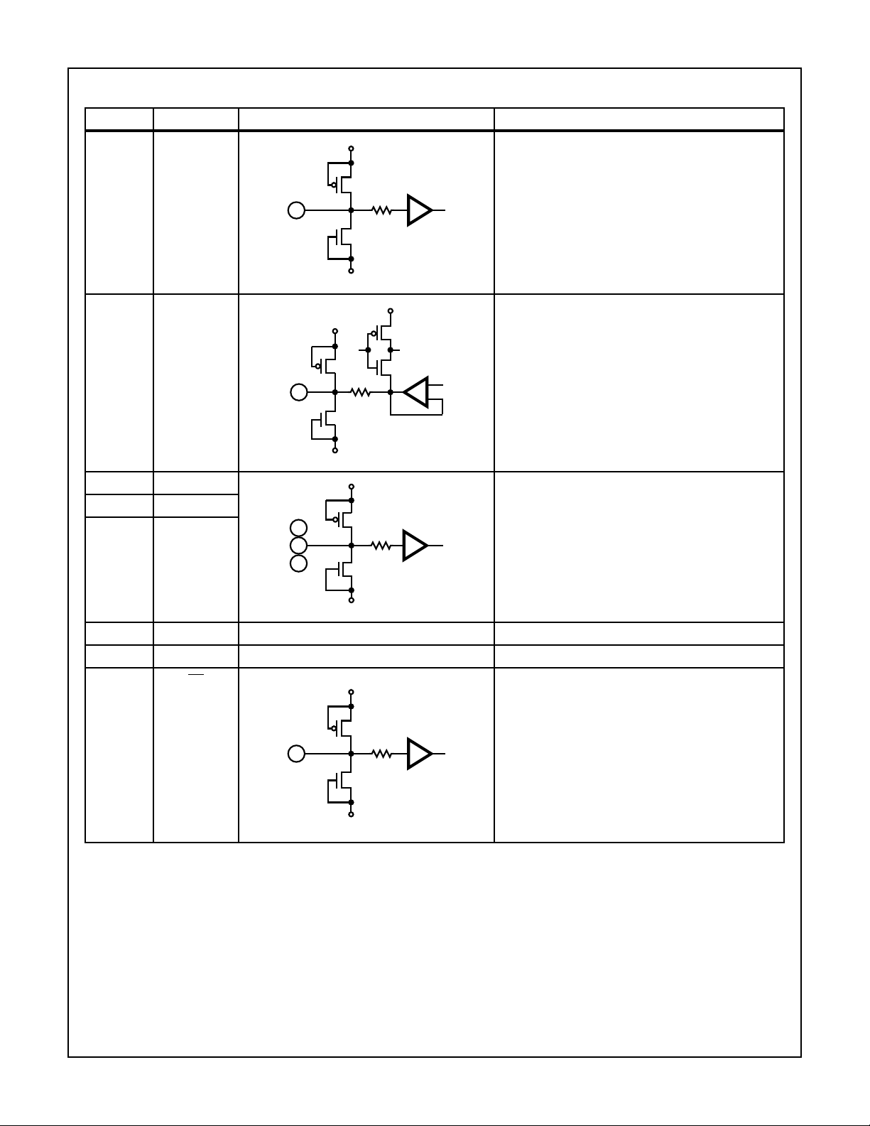
Pin Descriptions
PIN NO. SYMBOL EQUIVALENT CIRCUIT DESCRIPTION
1 to 8 R0 to R7 Digital Input.
9 to 16 G0 to G7
17 to 24 B0 to B7
1
TO
25
DV
DV
DD
SS
10-2
VB
HI2304
Pin Descriptions
(Continued)
PIN NO. SYMBOL EQUIVALENT CIRCUIT DESCRIPTION
25 BLK Blanking pin. No signal at “H” (Output 0V)
25
32 VB Connect a capacitor of about 0.1µF.
DV
32
DV
27 RCK Clock Pin.
DD
SS
DV
DV
DV
DD
SS
DD
DV
DD
Output condition at “L”.
+
-
28 GCK
29 BCK
27
28
29
30, 31 DV
33 AV
26
CE
SS
SS
DV
SS
Digital GND.
Analog GND.
Chip Enable Pin. No signal (Output 0V) at “H” and
DV
DD
26
DV
SS
minimizes power consumption.
10-3
HI2304
Pin Descriptions
(Continued)
PIN NO. SYMBOL EQUIVALENT CIRCUIT DESCRIPTION
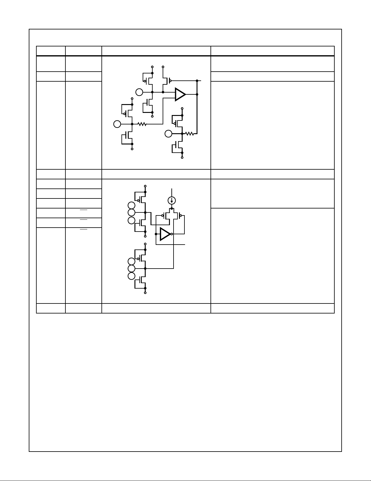
35 I
34 V
REF
REF
AV
DD
AV
DD
Connect a resistance 16 times “16R” that of output
resistance value “R”.
Set full scale output value.
42 VG Connect a capacitor of about 0.1µF.
35
AV
DD
AV
SS
34
AV
SS
43 to 46 AV
37 RO Current output pin. Voltage output can be obtained by
DD
AV
DD
39 GO
41 BO
36 RO Inverted current output pin. Normally dropped to analog
38 GO
40 BO
37
39
41
AV
SS
AV
DD
+
-
AV
DD
42
AV
SS
Analog VDD.
connecting a resistance.
GND.
47, 48 DV
DD
36
38
40
AV
SS
Digital VDD.
10-4

HI2304
Absolute Maximum Ratings T
Supply Voltage (VDD). . . . . . . . . . . . . . . . . . . . . . . . . . . . . . . . . . 7V
Input Voltage (VIN) . . . . . . . . . . . . . . . . . . . . . . . . . . . . . VDD to V
Output Current (I
(Every Each Channel)
). . . . . . . . . . . . . . . . . . . . . . . . . .0mA to 15mA
OUT
Operating Conditions
Temperature Range (T
Supply Voltage
AVDD, AVSS . . . . . . . . . . . . . . . . . . . . . . . . . . . . . . . .3.0V to 3.6V
DVDD, DVSS. . . . . . . . . . . . . . . . . . . . . . . . . . . . . . . .3.0V to 3.6V
Reference Input Voltage (V
Clock Pulse Width
t
. . . . . . . . . . . . . . . . . . . . . . . . . . . . . . . . . . . . . . . 25ns (Min)
PW1
t
. . . . . . . . . . . . . . . . . . . . . . . . . . . . . . . . . . . . . . . 25ns (Min)
PW0
CAUTION: Stresses above those listed in “Absolute Maxim um Ratings” ma y cause permanent damage to the device . This is a stress only rating and oper ation of
the device at these or any other conditions above those indicated in the operational sections of this specification is not implied.
NOTE:
1. θJA is measured with the component mounted on an evaluation PC board in free air.
) . . . . . . . . . . . . . . . . . . . . -20oC to 75oC
OPR
). . . . . . . . . . . . . . . . . . . . . . . . 1.2V
REF
Electrical Specifications f
PARAMETER SYMBOL TEST CONDITIONS MIN TYP MAX UNITS
Resolution
Maximum Conversion Speed f
Linearity Error INL -2.5 - 2.5 LSB
Differential Linearity Error DNL -0.5 - 0.5 LSB
Full Scale Output Voltage V
Full Scale Output Ratio (Note 1) F
Full Scale Output Current I
Offset Output Voltage V
Power supply Current I
Digital Input
Current
Set Up Time t
Hold Time t
Propagation Delay Time t
Glitch Energy GE - 150 - pV/s
Crosstalk CT 1MHz Sine Wave Output - 53 - dB
NOTE:
2. Full Scale Output Ratio = x 100(%).
H Level I
L Level I
-------------------------------------------------------------------------------------------------------------------------------
Average of the full-scale voltage of the channels
=25oC Thermal Information
A
Thermal Resistance (Typical, Note 1) θJA (oC/W)
SS
MQFP Package. . . . . . . . . . . . . . . . . . . . . . . . . . . . 104
Maximum Junction Temperature (Plastic Package) . . . . . . . . 150oC
Maximum Storage Temperature (T
Maximum Lead Temperature (Soldering 10s). . . . . . . . . . . . . 300oC
(Lead Tips Only)
= 20MHz, VDD= 3.3V, R
CLK
n
MAX
FS
SR
FS
OS
DD
IH
IL
S
H
PD
Full scale voltage of channel
14.3MHz, at Color Bar Data input - 15 - mA
= 330Ω, V
OUT
REF
1–
= 1.2V, R
) . . . . . . . . . .-65oC to 150oC
STG
= 5.1kΩ, TA = 25oC
IRF
- 8 - Bit
20 - - MHz
1.12 1.24 1.36 V
0 1.5 3 %
- 3.8 - mA
--1mV
--5µA
-5 - - µA
7--ns
3--ns
-20- ns
I/O Chart
(When Full Scale Output Voltage at 2.00V)
INPUT CODE OUTPUT VOLTAGE
MSB LSB
11111111 1.2V
•
•
•
10000000 0.6V
•
•
•
00000000 0V
10-5

HI2304
Timing Diagram
CLK
DAT A
D/A OUT
Typical Application Circuit
DV
(LSB)
1
2
3
(MSB)
(LSB)
4
5
6
7
8
9
10
11
12
R (RED) IN
t
PW1tPW1
tSt
H
t
PD
AV
DD
DD
48 47 46 45 44 43 42 41 40 39 38 37
13 14 15 16 17 18 19 20 21 22 23 24
0.1µ
HI2304
t
t
S
H
t
PD
t
S
(BCK)
(GCK)
(RCK)
t
H
100%
50%
t
PD
0%
B (BLUE) OUT
330
AV
SS
G (GREEN) OUT
330
AV
SS
R (RED) OUT
330
AV
1.2V
0.1µ
DV
DV
SS
1K
SS
SS
AV
AV
DD
SS
5.1K
AV
CLOCK IN
SS
36
35
34
33
32
31
30
29
28
27
26
25
G (GREEN) IN
(MSB)
(LSB)
(MSB)
B (BLUE) IN
10-6

Notes On Operation
• How to Select the Output Resistance
The HI2304 is a current output D/A converter. To obtain
the output voltage, connect the resistance to IO pin (RO,
GO, BO). For specifications we have:
Output Full Scale Voltage VFS = 1.2 [V].
Output Full Scale Current I
= 3.8 [mA].
FS
Calculate the output resistance value from the relation of
V
= IFS x R. Also, 16 times resistance of the output
FS
resistance is connected to reference current pin I
REF
some cases, however, this turns out to be a value that
does not actually exist. In such a case a value close to it
can be used as a substitute. Here, please note that V
becomes VFS = V
nected to IO while R is connected to I
x 16R/R. R is the resistance con-
REF
. Increasing the
REF
Test Circuits
HI2304
resistance value can curb power consumption. On the
other hand, glitch energy and data settling time will
inversely increase. Set the most suitable value according
to the desired application.
• Phase Relation Between Data and Clock
To obtain the expected performance as a D/A conver ter, it
is necessary to set properly the phase relation between
data and clock, applied from the exterior . Be sure to satisfy
the provisions of the set up time (t
stipulated in the Electrical Characteristics.
. In
•V
DD
, V
SS
To reduce noise effects, separate analog and digital systems
in the device periphery. For V
FS
log, bypass respective GNDs by using a cer amic capacitor of
DD
about 0.1µF, as close as possible to the pin.
) and hold time (tH) as
S
pins, both digital and ana-
CLK
1MHz
SQUARE
WAVE
CLK
20MHz
SQUARE
WAVE
8-BIT
COUNTER
WITH
LATCH
DV
0.1µ
SS
25
26
32
27
28
29
R0 TO R7
1 TO 8
G0 TO G7
9 TO 16
B0 TO B7
17 TO 24
BLK
CE
VB
HI2304
RCK
GCK
BCK
V
REF
I
REF
R0
G0
B0
VG
37
39
41
42
34
35
FIGURE 1. MAXIMUM CONVERSION RATE TEST CIRCUIT
8-BIT
COUNTER
WITH
LATCH
DELAY
CONTROLLER
DELAY
CONTROLLER
DV
SS
0.1µ
25
26
32
27
28
29
R0 TO R7
1 TO 8
G0 TO G7
9 TO 16
B0 TO B7
17 TO 24
BLK
CE
VB
HI2304
RCK
GCK
BCK
R0
G0
B0
VG
V
REF
I
REF
AV
AV
SS
SS
AV
0.1µ
5.1K
37
39
41
42
34
35
330
330
330
SS
AV
AV
AV
AV
AV
330
SS
330
SS
330
SS
DD
0.1µ
5.1K
OSCILLOSCOPE
DD
1K
AV
SS
1K
AV
SS
OSCILLOSCOPE
FIGURE 2. SET-UP HOLD TIME GLITCH ENERGY TEST CIRCUIT
10-7

HI2304
Test Circuits
(Continued)
DIGITAL
WAVEFORM
GENERATOR
R0 TO R7
1 TO 8
G0 TO G7
9 TO 16
B0 TO B7
17 TO 24
25
BLK
26
CE
32
VB
RCK
27
28
GCK
29
BCK
HI2304
37
R0
330
AV
SS
39
G0
330
AV
SS
41
B0
330
AV
SS
AV
DD
42
VG
0.1µ
34
V
REF
35
I
REF
5.1K
AV
1K
SS
CLK
20MHz
SQUARE
WAVE
ALL “1”
0.1µ
DV
SS
FIGURE 3. CROSSTALK TEST CIRCUIT (See Figure 7)
SPECTRUM
ANALYZER
CONTROLLER
SQUARE
R0 TO R7
CLK
20MHz
WAVE
DV
SS
0.1µ
1 TO 8
G0 TO G7
9 TO 16
B0 TO B7
17 TO 24
25
BLK
26
CE
32
VB
RCK
27
28
GCK
29
BCK
HI2304
37
R0
330
AV
SS
39
G0
330
AV
SS
41
B0
330
AV
SS
AV
DD
42
VG
0.1µ
34
V
REF
35
I
REF
5.1K
AV
FIGURE 4. DC CHARACTERISTICS TEST CIRCUIT
DVM
1K
SS
10-8

HI2304
Test Circuits
(Continued)
FREQUENCY
DEMULTIPLIER
CLK
1MHz
SQUARE
WAVE
R0 TO R7
DV
SS
0.1µ
1 TO 8
G0 TO G7
9 TO 16
B0 TO B7
17 TO 24
25
BLK
26
CE
32
VB
27
RCK
28
GCK
29
BCK
HI2304
37
R0
330
AV
SS
39
G0
330
AV
SS
41
B0
330
AV
SS
AV
DD
42
VG
0.1µ
34
V
REF
35
I
REF
5.1K
AV
1K
SS
FIGURE 5. PROPAGATION DELAY TIME TEST CIRCUIT
OSCILLOSCOPE
DIGITAL
WAVEFORM
GENERATOR
SQUARE
ALL “1”
R0 TO R7
CLK
20MHz
WAVE
ALL “1”
0.1µ
DV
SS
1 TO 8
G0 TO G7
9 TO 16
B0 TO B7
17 TO 24
25
BLK
26
CE
32
VB
RCK
27
28
GCK
29
BCK
HI2304
37
R0
39
G0
41
B0
42
VG
34
V
REF
35
I
REF
FIGURE 6. SNR TEST CIRCUIT (See Figure 8)
AV
AV
AV
AV
330
SS
330
SS
330
SS
DD
0.1µ
AV
SPECTRUM
ANALYZER
SNR: Difference between primary
component and secondary distortion.
1K
SS
10-9

Typical Performance Curves
HI2304
80
60
40
CROSSTALK (dB)
20
0
1.27
1.26
80
60
40
SNR (dB)
20
0
0.1M 1M 10M
OUTPUT FREQUENCY (Hz)
0.1M 1M 10M
OUTPUT FREQUENCY (Hz)
FIGURE 7. CROSSTALK FIGURE 8. SNR (DIFFERENCE BETWEEN PRIMARY
COMPONENT AND SECONDARY DISTORTION)
20
10
OUTPUT FULL SCALE VOLTAGE (V)
0
-25 0 25 50 75
AMBIENT TEMPERATURE (
o
C)
FIGURE 9. OUTPUT FULL SCALE VOLTAGE vs AMBIENT
TEMPERATURE
400
200
GLITCH ENERGY (pV/s)
0
200 400 600
FIGURE 11. OUTPUT RESISTANCE vs GLITCH ENERGY
CURRENT CONSUMPTION (mA)
0
10K 100K 1M 10M
OUTPUT FREQUENCY (Hz)
FIGURE 10. OUTPUT FREQUENCY vs CURRENT
CONSUMPTION
10-10

HI2304
Reference Measurement Condition and
Description
AVDD = 3.3V.
= 3.3V.
DV
DD
= 1.2V.
V
REF
= 5.1kΩ.
R
IRF
= 25oC.
T
A
Figure 7 and Figure 8 refer to the measurement circuit.
Figure 9 is input data = all 1.
Figure 10 is input data = output of incremental counter,
current consumption is total of 3ch.
10-11
 Loading...