

HI1177
Data Sheet January 1999 File Number 4114.2
8-Bit, 40MSPS, 2-Channel D/A Converter
The HI1177 is a dual 8-bit CMOS digital-to-analog converter.
It has input/output equivalent to 2 channels of Y and C for
video use or I and Q for modulators.
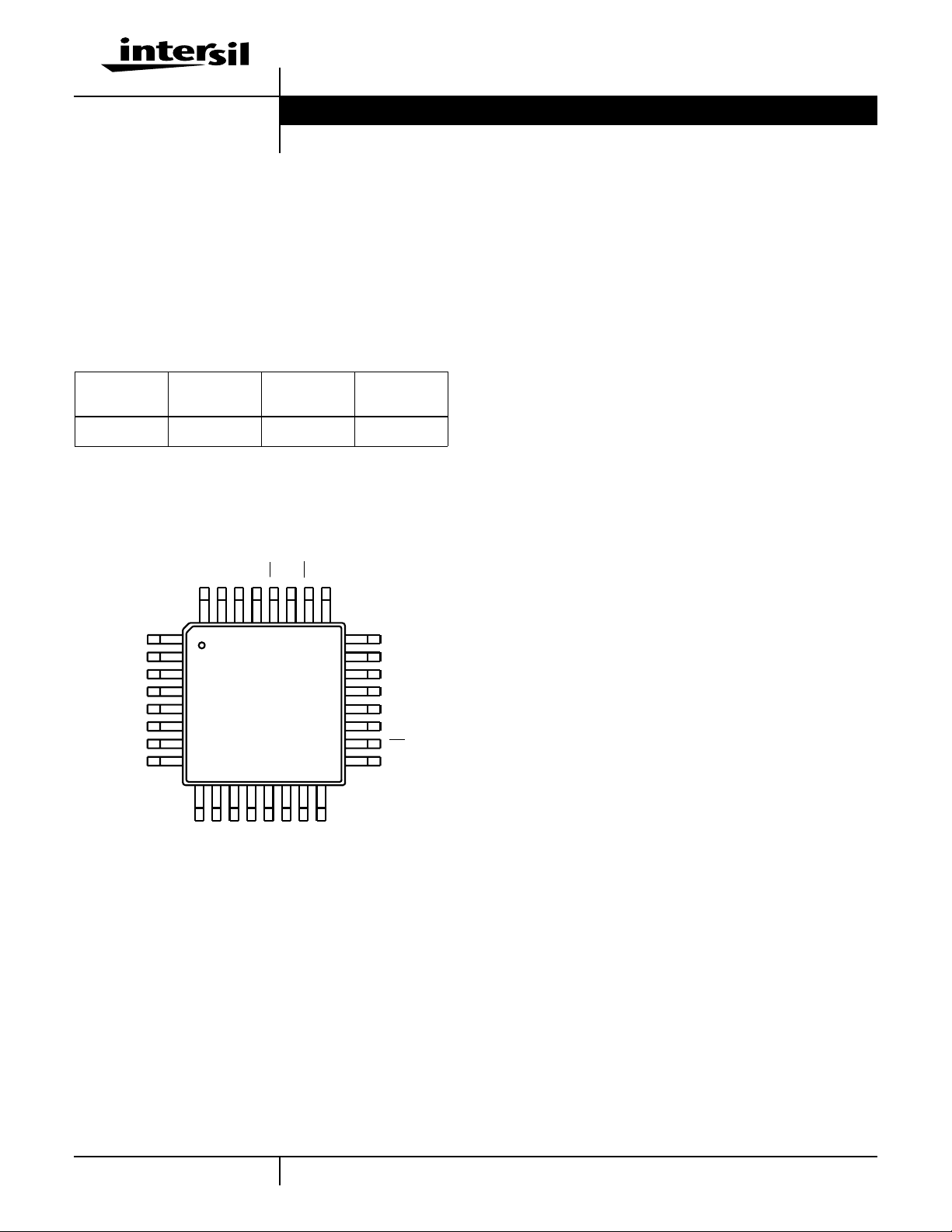
The HI1177 is available in the industrial temperature range
and is supplied in a 32 lead plastic metric quad flatpack
(MQFP) package.
Ordering Information
PART
NUMBER
HI1177JCQ -40 to 85 32 Ld MQFP Q32.7x7-S
TEMP.
RANGE (oC) PACKAGE PKG. NO.
Pinout
HI1177
(MQFP)
TOP VIEW
DD
Y0
Y1
Y2
Y3
Y4
Y5
Y6
Y7
DD
G
V
DV
32 31 30 29 28 27 26 25
1
2
3
4
5
6
7
8
AV
YO
YO
CO
CO
161514131211109
24
23
22
21
20
19
18
17
REF
V
I
REF
AV
V
B
DV
CCK
YCK
CE
BLK
SS
SS
Features
• Resolution . . . . . . . . . . . . . . . . . . . . . . . . . . . . . . . . . 8-Bit
• Maximum Conversion Speed. . . . . . . . . . . . . . . . . 40MHz
• YC 2-Channel Input/Output
• Differential Linearity Error. . . . . . . . . . . . . . . . . ± 0.3 LSB
• Low Power Consumption . . . . . . . . . . . . . . . . . . . .160mW
(200Ω Load for 2V
P-P
Output)
• Power Supply . . . . . . . . . . . . . . . . . . . . . . . . . . +5V Single
• Power-Down Mode
• Low Glitch Noise
• Direct Replacment for Sony CXD1177
Applications
• I/Q Modulation
• YC Video
• Digital TV
• Wireless Transmitters
C0
C1
C2
C3
C7
C6
C5
C4
5
CAUTION: These devices are sensitive to electrostatic discharge; follow proper IC Handling Procedures.
1-888-INTERSIL or 321-724-7143
| Copyright © Intersil Corporation 1999
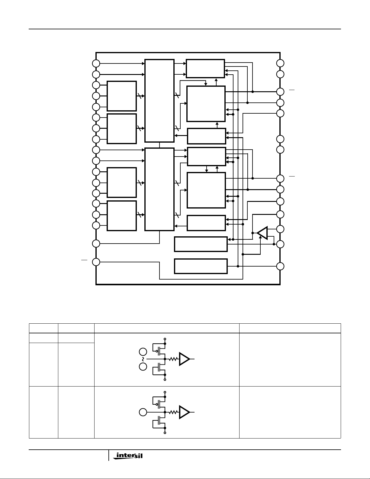
Functional Block Diagram
HI1177
(LSB) Y0
Y1
Y2
Y3
Y4
Y5
Y6
Y7
(LSB) C0
C1
C2
C3
C4
C5
C6
C7
BLK
1
2
3
4
DECODER
5
6
7
DECODER
8
9
10
11
DECODER
12
13
14
15
DECODER
16
17
LATCHES
LATCHES
2 LSBs
CURRENT
CELLS
6 MSBs
CURRENT
CELLS
CLOCK
GENERATOR
2 LSBs
CURRENT
CELLS
6 MSBs
CURRENT
CELLS
CLOCK
GENERATOR
CURRENT CELLS
(FOR FULL SCALE)
-
+
DV
32
DD
31
AV
DD
28
Y0
29
Y0
19
YCK
23
AV
SS
21
DV
SS
C0
26
27
C0
20
CCK
30
V
G
25
V
REF
24
I
REF
18
CE
BIAS VOLTAGE
GENERATOR
22
V
B
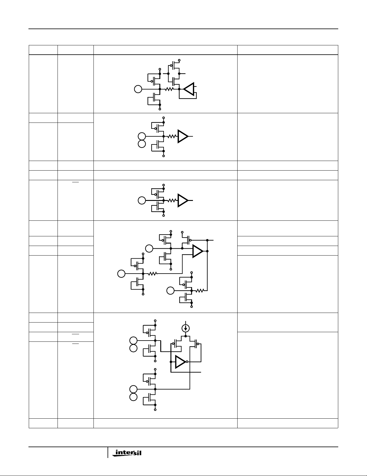
Pin Descriptions
NUMBER SYMBOL EQUIVALENT CIRCUIT DESCRIPTION
1 to 8 Y0 to Y7 Digital Input.
9 to 16 C0 to C7
1
16
17 BLK Blanking pin. No signal at “H” (Output 0V).
17
DV
DV
DV
DV
DD
SS
DD
SS
Output condition at “L”.
6
HI1177
Pin Descriptions (Continued)
NUMBER SYMBOL EQUIVALENT CIRCUIT DESCRIPTION
22 V
B
DV
DD
22
DV
19 YCK Clock pin. Moreover all input pins are
20 CLK
19
20
21 DV
23 AV
SS
SS
18 CE Chip enable pin. No signal (Output 0V) at “H”
18
DV
DV
DV
SS
DD
SS
DD
DV
DD
+
-
Connect a capacitor of about 0.1µF.
TTL-CMOS compatible.
Digital GND.
Analog GND.
and minimizes power consumption.
DV
SS
24 I
25 V
30 V
31 AV
27 CO Current output pin. Voltage output can be ob-
REF
REF
G
DD
AV
DD
AV
DD
+
24
AV
DD
-
AV
25
AV
SS
AV
SS
30
DD
AV
AV
DD
SS
29 YO
26 CO Inverted current output pin. Normally dropped
28 YO
27
29
AV
SS
AV
DD
26
28
Connect a resistance 16 times “16R” that of
output resistance value “R”.
Set full scale output value.
Connect a capacitor of about 0.1µF.
Analog VDD.
tained by connecting a resistance.
to analog GND.
32 DV
DD
AV
SS
Digital VDD.
7

HI1177
Absolute Maximum Ratings T
Supply Voltage, VDD . . . . . . . . . . . . . . . . . . . . . . . . . . . . . . . . . . .7V
Input Voltage, VIN . . . . . . . . . . . . . . . . . . . . . . . . . . . . . VDD to V
Output Current (For Each Channel), l
Operating Conditions
Supply Voltage
= 25oC Thermal Information
A
Thermal Resistance (Typical, Note 7) θJA (oC/W)
. . . . . . . . . .0mA to 15mA
OUT
SS
MQFP Package . . . . . . . . . . . . . . . . . . . . . . . . . . . . 122
Maximum Junction Temperature (Plastic Package) . . . . . . . .150oC
Maximum Storage Temperature Range. . . . . . . . . . -65oC to 150oC
Maximum Lead Temperature (Soldering 10s) . . . . . . . . . . . . .300oC
(MQFP - Lead Tips Only)
AVDD, AVSS. . . . . . . . . . . . . . . . . . . . . . . . . . . . . .4.75V to 5.25V
DVDD, DVSS. . . . . . . . . . . . . . . . . . . . . . . . . . . . . .4.75V to 5.25V
Reference Input Voltage, V
. . . . . . . . . . . . . . . . . . . . . . . . . 2.0V
REF
Clock Pulse Width
t
. . . . . . . . . . . . . . . . . . . . . . . . . . . . . . . . . . . . . .12.5ns (Min)
PW1
t
. . . . . . . . . . . . . . . . . . . . . . . . . . . . . . . . . . . . . .12.5ns (Min)
PW0
Temperature Range, T
CAUTION: Stresses above those listed in “Absolute Maximum Ratings” may cause permanent damage to the device. This is a stress only rating and operation of the
device at these or any other conditions above those indicated in the operational sections of this specification is not implied.
. . . . . . . . . . . . . . . . . . . . -40oC to 85oC
OPR
NOTE:
1. θJA is measured with the component mounted on an evaluation PC board in free air.
Electrical Specifications f
= 40MHz, VDD = 5V, R
CLK
= 200Ω, V
OUT
= 2.0V, TA = 25oC
REF
TEST
PARAMETER SYMBOL
TEST
CONDITIONS
LEVEL
OR NOTES MIN TYP MAX UNITS
Resolution n - 8 - bit
Maximum Conversion Speed f
Linearity Error E
Differential Linearity Error E
Full Scale Output Voltage V
Full Scale Output Ratio F
Full Scale Output Current I
Offset Output Voltage V
Power Supply Current I
Digital Input
Current
High Level I
Low Level I
Setup Time t
Hold Time t
Propagation Delay Time t
MAX
L
D
FS
SR
FS
OS
DD
IH
IL
S
H
PD
Glitch Energy GE R
Note 1 0 1.5 3 %
14.3MHz, at Color Bar Data Input - - 32 mA
= 75Ω - 30 - pV-s
OUT
40 - - MHz
-2.5 - 2.5 LSB
-0.3 - 0.3 LSB
1.9 2.0 2.2 V
-1015mA
--1mV
--5µA
-5 - - µA
5--ns
10 - - ns
-10-ns
Cross Talk CT 1MHz Sin Wave Output - 57 - dB
NOTE:
1. Full scale output ratio = .
-------------------------------------------------------------------------------------------------------------------------------
Average of the full-scale voltage of the channels
Full-scale voltage of channel
1–()x100(%)
I/O Correspondence Table (Output Full Scale Voltage: 2V)
INPUT CODE OUTPUT VOLTAGE
MSB LSB
11111111 2.0V
•
•
•
10000000 1.0V
•
•
•
00000000 0V
8

Timing Diagram
HI1177
CLK
DAT A
D/AOUT
Test Circuits
t
PW1
t
S
t
HL
t
PD
t
PW0
t
S
t
HL
t
PD
t
S
t
HL
100%
50%
t
PD
0%
FIGURE 1.
CLK
40MHz
SQUARE
WAVE
8-BIT
COUNTER
WITH
LATCH
Y0 ~ Y7
1
~ 8
~ C7
C0
9
~ 18
BLK
17
CE
18
0.1µ
DV
SS
V
22
B
YCK
19
CCK
20
V
I
FIGURE 2. MAXIMUM CONVERSION
Y0
C0
V
REF
REF
29
200
AV
SS
27
200
AV
SS
30
G
0.1µ
25
24
3.3K
OSCILLOSCOPE
AV
DD
1K
AV
SS
9

Test Circuits (Continued)
COUNTER
CONTROLLER
CLK
1MHz
SQUARE
WAVE
CONTROLLER
8-BIT
WITH
LATCH
DELAY
DELAY
HI1177
29
Y0 ~ Y7
1
~ 8
~ C7
C0
9
~ 18
17
BLK
18
SS
CE
22
V
B
19
YCK
20
CCK
0.1µ
DV
FIGURE 3. SETUP HOLD TIME AND GLITCH ENERGY
Y0
27
C0
V
30
G
25
V
REF
I
24
REF
AV
AV
0.1µ
1.2K
SS
SS
75
OSCILLOSCOPE
75
AV
DD
1K
AV
SS
DIGITAL
WAVEFORM
GENERATOR
CLK
40MHz
SQUARE
WAVE
CLK
40MHz
SQUARE
WAVE
CONTROLLER
ALL “1”
0.1µ
DV
Y0 ~ Y7
~ 8
1
~ C7
C0
9
~ 18
BLK
17
CE
18
0.1µ
DV
SS
V
22
B
YCK
19
CCK
20
FIGURE 4. CROSSTALK
Y0 ~ Y7
~ 8
1
~ C7
C0
9
~ 18
BLK
17
CE
18
V
22
B
SS
YCK
19
CCK
20
29
Y0
200
AV
AV
DD
SS
DD
SS
SPECTRUM
ANALIZER
DVM
AV
SS
27
C0
200
AV
SS
30
V
G
V
REF
I
REF
29
Y0
27
C0
30
V
G
25
V
REF
I
24
REF
0.1µ
25
24
3.3K
200
AV
SS
200
AV
SS
0.1µ
3.3K
1K
AV
1K
AV
10
FIGURE 5. DC CHARACTERISTICS

Test Circuits (Continued)
FREQUENCY
DEMULTIPLIER
CLK
10MHz
SQUARE
WAVE
Typical Performance Curves
HI1177
29
200
Y0
27
C0
V
30
G
V
25
REF
I
24
REF
Y0 ~ Y7
1
~ 8
~ C7
C0
9
~ 18
BLK
17
CE
18
0.1µ
DV
SS
V
22
B
YCK
19
CCK
20
FIGURE 6. PROPAGATION DELAY TIME
200
AV
200
AV
0.1µ
3.3K
SS
SS
OSCILLOSCOPE
AV
DD
1K
AV
SS
2
1
VDD = 5.0V
R = 200Ω
, OUTPUT FULL SCALE VOLTAGE (V)
FS
V
V
REF
16R = 3.3kΩ
T
= 25oC
A
12
, REFERENCE VOLTAGE (V)
FIGURE 7. OUTPUT FULL SCALE VOLTAGE vs REFERENCE
VOLTAGE
2.0
1.9
VDD = 5V
V
= 2V
REF
R = 200Ω
16R = 3.3kΩ
0
OUTPUT FULL SCALE VOLTAGE (V)
-25 2505075
AMBIENT TEMPERATURE (
o
C)
100
FIGURE 9. OUTPUT FULL SCALE VOLTAGE vs AMBIENT
TEMPERATURE
100
100 200
OUTPUT RESISTANCE (Ω)
FIGURE 8. GLITCH ENERGY vs OUTPUT RESISTANCE
60
50
CROSSTALK (dB)
40
100K 10M1M
OUTPUT FREQUENCY (Hz)
FIGURE 10. CROSSTALK vs OUTPUT FREQUENCY
11

Application Circuit
HI1177
Y IN
(LSB)
(MSB)
Y OUT
200
AV
SS
DV
DD
AV
DD
0.1µF
31
1
2
3
4
5
6
7
8
9 10 11 12 13 14 15 16
29 2832
30
C OUT
200
AV
SS
AV
DD
AV
SS
25
2627
1K
AV
SS
24
23
22
21
20
19
18
17
(MSB)(LSB)
3.3K
AV
0.1µF
DV
DV
SS
SS
CLOCK
SS
C IN
FIGURE 11.
Operation
• How to select the output resistance:
- The HI1177 is a D/A converter of the current output type.
To obtain the output voltage connect the resistance to IO
pin (Y0, C0). For specifications we have:
Output full scale voltage VFS = less than 2V
Output full scale current I
= less than 15mA
FS
- Calculate the output resistance value from the relation
of V
FS=IFS
resistance is connected to reference current pin I
X R. Also, 16 times resistance of the output
.In
REF
some cases, however, this turns out to be a value that
does not actually exist. In such a case a value close to it
can be used as a substitute. Here please note that V
becomes VFS=V
connected to IO while R’ is connected to I
X 16R/R’. R is the resistance
REF
REF
FS
. Increasing the resistance value can curb power consumption.
On the other hand glitch energy and data settling time
will inversely increase. Set the most suitable value
according to the desired application.
All Intersil semiconductor products are manufactured, assembled and tested under ISO9000 quality systems certification.
Intersil semiconductor products are sold by description only .Intersil Corporation reserves the right to make changes in circuit design and/or specifications at any time without notice. Accordingly, the reader is cautioned to verify that data sheets are current before placing orders. Information furnished by Intersil is believed to be accurate and
reliable. Howe ver, no responsibility is assumed by Intersil or its subsidiaries for its use; nor for any infringements of patents or other rights of third parties which may result
from its use. No license is granted by implication or otherwise under any patent or patent rights of Intersil or its subsidiaries.
For information regarding Intersil Corporation and its products, see web site http://www.intersil.com
• Phase relation between data and clock:
- To obtain the expected performance as a D/A converter,it
is necessary to set properly the phase relation between
data and clock applied from the exterior . Be sure to
satisfy the provisions of the set up time (t
(t
) as stipulated in the Electrical Characteristics.
H
, VSS:
•V
DD
) and hold time
S
- To reduce noise effects separate analog and digital
systems in the device periphery. For V
pins, both
DD
digital and analog, bypass respective GNDs by using a
ceramic capacitor of about 0.1µF, as close as possible
to the pin.
12
 Loading...