

HI1166
September 1998 File Number 3579.4
8-Bit, 250 MSPS, Flash A/D Converter
The HI1166 is an 8-bit, ultra high speed, flash Analog-toDigital converter IC capable of digitizing analog signals at a
maximum rate of 250 MSPS. The digital I/O levels of the
converter are compatible with ECL 100K/10KH/10K.
Applications
• Spectrum Analyzers • Video Digitizing
• Radar Systems • Communication Systems
• Direct RF Down-Conversion • Digital Oscilloscopes
Ordering Information
PART
NUMBER
HI1166AIL -20 to 100 68 Ld CLCC J68.A
HI1166-EV 25 Evaluation Board
TEMP. RANGE
(oC) PACKAGE PKG. NO.
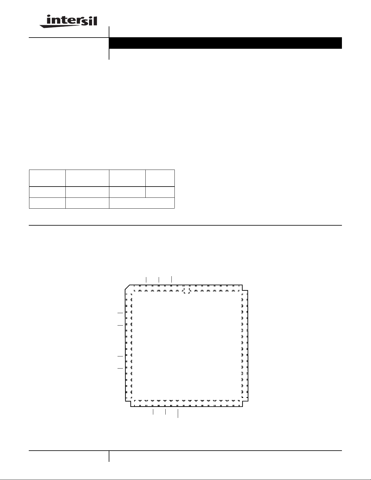
Pinout
Features
• Differential Linearity Error . . . . . . . . . . ±0.5 LSB or Less
• Integral Linearity Error . . . . . . . . . . . . . ±0.5 LSB or Less
• Built-In Integral Linearity Compensation Circuit
• Ultra High Speed Operation with Maximum
Conversion Rate (Min) . . . . . . . . . . . . . . . . . . . 250 MSPS
• Low Input Capacitance 18pF (Typ)
• Wide Analog Input Bandwidth
(Min for Full Scale Input) . . . . . . . . . . . . . . . . . . . 250MHz
• Single Power Supply . . . . . . . . . . . . . . . . . . . . . . . . -5.2V
• Low Power Consumption . . . . . . . . . . . . . . . . . 1.4W (Typ)
• Low Error Rate
• Capable of Driving 50Ω Loads
• Evaluation Board Available
• Direct Replacement for Sony CXA1166K
HI1166
(CLCC)
TOP VIEW
NC
NC
D2
D2
D3
D3
DGND2
DGND2
DGND1
D4
D4
D5
D5
NC
NC
NC
NC
EEAVEE
AV
RTSVRT
RBS
V
DVEED1D1D0D0ORORLINVNCAVEEAVEEV
NC
876543216867666564636261
9
10
11
12
13
14
15
16
17
18
19
20
21
22
23
24
25
26
27 28 29 30 31 32 33 34 35 36 37 38 39 40 41 42 43
EE
NC
D6D6D7
DV
D7
MINV
CLK
CLK
NC
EE
NC
AV
AGND
60
NC
59
NC
58
AV
EE
57
NC
56
AGND
55
V
IN1
54
V
IN1
53
AGND
52
V
RM
51
AGND
50
V
IN2
49
V
IN2
48
AGND
47
NC
46
NC
45
NC
44
NC
EE
RB
NC
V
AV
AGND
1
CAUTION: These devices are sensitive to electrostatic discharge; follow proper IC Handling Procedures.
http://www.intersil.com or 407-727-9207 | Copyright © Intersil Corporation 1999
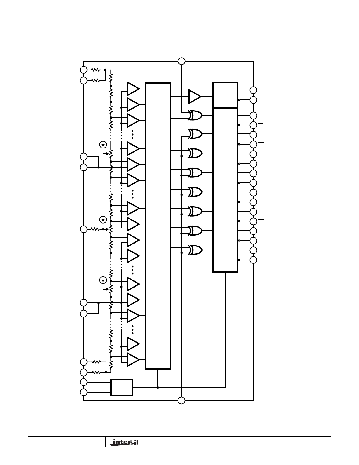
Functional Block Diagram
R1
64
V
RT
V
65
RTS
V
V
IN1
RM
R2
54
55
R3
52
R/2
R
R
R
R
R
R
R
R
R
COMPARATOR
0
1
2
63
64
65
126
127
ENCODE
LOGIC
128
129
HI1166
MINV
33
OUTPUT
2
3
31
32
29
30
21
22
19
20
14
15
12
13
6
7
4
5
OR
OR
D7 (MSB)
D7
D6
D6
D5
D5
D4
D4
D3
D3
D2
D2
D1
D1
D0 (LSB)
D0
V
V
IN2
RBS
V
RB
CLK
CLK
R
191
R
49
50
R4
39
40
R5
35
34
192
R
193
R
254
R
255
R/2
CLOCK
DRIVER
1
LINV
2
HI1166
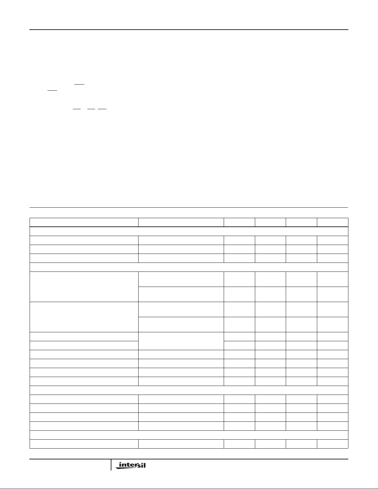
Absolute Maximum Ratings T
Supply Voltage (AVEE, DVEE) . . . . . . . . . . . . . . . . . . . .-7V to +0.5V
Analog Input Voltage (VIN). . . . . . . . . . . . . . . . . . . . . -2.7V to +0.5V
Reference Input Voltage
VRT, VRB, VRM. . . . . . . . . . . . . . . . . . . . . . . . . . . . -2.7V to +0.5V
|VRT-VRB|. . . . . . . . . . . . . . . . . . . . . . . . . . . . . . . . . . . . . . . 2.5V
Digital Input Voltage
= 25oC Thermal Information
A
Thermal Resistance (Typical, Note 2) θ
CLCC Package. . . . . . . . . . . . . . . . . . . 38 10
Maximum Power Dissipation . . . . . . . . . . . . . . . . . . . . . . . . . . .2.1W
Maximum Junction Temperature . . . . . . . . . . . . . . . . . . . . . . .175oC
Maximum Storage Temperature Range (T
Maximum Lead Temperature (Soldering, 10s). . . . . . . . . . . . .300oC
o
C/W θ
JA
). . . . -65oC to 150oC
STG
JC
o
C/W
MINV, LINV, CLK,CLK. . . . . . . . . . . . . . . . . . . . . . . .-4V to +0.5V
|CLK-CLK| . . . . . . . . . . . . . . . . . . . . . . . . . . . . . . . . . . . . . . . 2.7V
VRM Pin Input Current (I
) . . . . . . . . . . . . . . . . . . -3mA to +3mA
VRM
Digital Output Current
(ID0 to ID7, IOR, ID0 to ID7, IOR) . . . . . . . . . . . . . -30mA to 0mA
Temperature Range, TA (Note 5) . . . . . . . . . . . . . . . -20oC to 100oC
TC . . . . . . . . . . . . . . . . . . . . . -20oC to 125oC
Operating Conditions (Note 1)
Supply Voltage MIN TYP MAX
AVEE, DVEE. . . . . . . . . . . . . . . . . . . . . . . -5.5V -5.2 -4.95V
AVEE - DVEE . . . . . . . . . . . . . . . . . . . . . . -0.05V 0 0.05V
AGND - DGND. . . . . . . . . . . . . . . . . . . . .-0.05V 0 0.05V
CAUTION: Stresses above those listed in “Absolute Maximum Ratings” may cause permanent damage to the device. This is a stress only rating and operationofthe
device at these or any other conditions above those indicated in the operational sections of this specification is not implied.
NOTES:
1. Electrical Specifications guaranteed within stated operating conditions.
2. θJA is measured with the component mounted on an evaluation PC board in free air.
Electrical Specifications T
= 25oC, AVEE = DVEE = -5.2V, VRT, V
A
PARAMETER TEST CONDITIONS MIN TYP MAX UNIT
SYSTEM PERFORMANCE
Resolution - 8 - Bits
Integral Linearity Error, INL f
= 250 MSPS - ±0.3 ±0.5 LSB
C
Differential Linearity Error, DNL fC = 250 MSPS - ±0.3 ±0.5 LSB
DYNAMIC CHARACTERISTICS
Signal to Noise Ratio, SINAD Input = 1kHz, Full Scale
RMS Signal
----------------------------------------------------------------- -=
RMS Noise Distortion+
fC = 250MHz
Input = 60kHz, Full Scale
fC = 250MHz
Error Rate Input = 50MHz, Full Scale
Error > 16 LSB, fC = 250MHz
Input = 62.499MHz, Full Scale
Error > 16 LSB, fC = 250MHz
Differential Gain Error, DG NTSC 40 IRE Mod.
Differential Phase Error, DP - 0.5 - Degree
Ramp, fC = 250 MSPS
Overrange Recovery Time - 1.0 - ns
Maximum Conversion Rate, f
Aperture Jitter, t
Sampling Delay, t
AJ
DS
C
ANALOG INPUT
Analog Input Capacitance, C
Analog Input Resistance, R
Input Bias Current, I
IN
IN
IN
Full Scale Input Bandwidth VIN = 2V
VIN - 1V + 0.07V
RMS
VIN = -1V 20 - 450 µA
P-P
REFERENCE INPUTS
Reference Resistance, R
REF
Reference Input Voltage MIN TYP MAX
VRT. . . . . . . . . . . . . . . . . . . . . . . . . . . . . . -0.1V -2 0.1V
VRB . . . . . . . . . . . . . . . . . . . . . . . . . . . . . -2.2V -2 -1.8V
Analog Input Voltage, VIN . . . . . . . . . . . . . . . . . . . . . . . .VRB to V
= 0V, VRB, V
RTS
= -2V (Note 1)
RBS
44 46 - dB
-37-dB
--10-9TPS
(Note 3)
-10-810
-6
TPS
(Note 3)
- 1.0 - %
250 - - MSPS
-9-ps
0.4 1.4 2.4 ns
-18-pF
50 120 - kΩ
200 250 - MHz
83 125 182 Ω
RT
3
HI1166
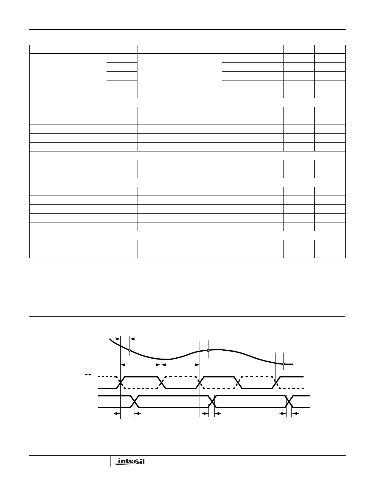
Electrical Specifications T
= 25oC, AVEE = DVEE = -5.2V, VRT, V
A
= 0V, VRB, V
RTS
= -2V (Note 1) (Continued)
RBS
PARAMETER TEST CONDITIONS MIN TYP MAX UNIT
Residual Resistance R1 Note 2 0.1 0.6 2.0 Ω
R2 300 500 700 Ω
R3 0.5 2.0 5.0 Ω
R4 300 500 700 Ω
R5 0.1 0.6 2.0 Ω
DIGITAL INPUTS
Logic H Level, V
Logic L Level, V
Logic H Current, I
Logic L Current, I
IH
IL
IH
IL
Input Connected to GND 0 - 70 µA
Input Connected to -2V -50 - 50 µA
-1.13 - - V
- - -1.5 V
Input Capacitance -4-pF
DIGITAL OUTPUTS
Logic H Level, V
Logic L Level, V
OH
OL
RL = 50Ω -1.0 - - V
RL = 50Ω - - -1.6 V
TIMING CHARACTERISTICS
H Pulse Width of Clock, t
L Pulse Width of Clock, t
Output Rise Time, t
Output Fall Time, t
Output Delay, t
r
f
OD
PW1
PW0
RL = 50Ω - 0.6 1.5 ns
RL = 50Ω - 0.6 1.5 ns
RL = 50Ω 1.8 2.5 3.2 ns
1.8 - - ns
1.8 - - ns
POWER SUPPLY CHARACTERISTICS
Supply Current, I
EE
Power Consumption, P
D
Note 4 - 1.4 1.9 W
-360 -270 - mA
NOTES:
1. Electrical Specifications guaranteed within stated operating conditions.
2. See Functional Block Diagram.
3. TPS: Times Per Sample.
4.
PD I
EEAAVEEIEEDDVEE
VRTVRB–()
-------------------------------------+•+•=
R
5. TAis specified instillairandwithoutheatsink. To extend temperature range, appropriate heat management techniques must be employed (See
2
REF
Figure 2).
Timing Diagram
ANALOG IN
DIGITAL OUT
CLK
CLK
t
SD
N
t
PW1
t
OD
t
PW0
20%
N + 1
80%
N + 2
NN - 1
t
r
80%
N + 1
20%
t
f
FIGURE 1.
4

Typical Performance Curves
HI1166
50
C/W)
o
(
JA
THERMAL RESISTANCEθ
40
30
0
SOCKET AMP:
173061-5 (WITHOUT HEAT SINK)
SOCKET AMP:
173257-3 (WITH HEAT SINK)
SOCKET:
YAMAICHI ELECTRONICS CO., LTD IC61-0684-048
1.0
2.0 3.0
AIR FLOW (m/s)
FIGURE 2. THERMAL RESISTANCE OF THE CONVERTER
MOUNTED ON A BOARD
150
125
100
25
20
15
INPUT CAPACITANCE (pF)
10
-2.0 -1.5 -1.0 -0.5 0
INPUT VOLTAGE (V)
FIGURE 3. VIN PIN CAPACITANCE vs VOLTAGE
CHARACTERISTICS
200
100
(µA)
IN
I
ANALOG INPUT RESISTANCE (kΩ)
10
-2.0 -1.5 -1.0 -0.5 0
INPUT VOLTAGE (V)
FIGURE 4. VIN PIN INPUT RESISTANCE vs VOLTAGE
CHARACTERISTICS
200
150
100
50
INPUT CURRENT (µA)
0
-50 0 50 100 150
CASE TEMPERATURE (
o
C)
FIGURE 6. VIN PIN INPUT CURRENT vs TEMPERATURE
CHARACTERISTICS
0
-2.0 -1.5 -1.0 -0.5 0
INPUT VOLTAGE (V)
FIGURE 5. VIN PIN INPUT CURRENT vs VOLTAGE
CHARACTERISTICS
-12
-14
-16
-18
-20
-22
RESISTOR STRING CURRENT (mA)
-24
-50 0 50 100 150
CASE TEMPERATURE (oC)
FIGURE 7. RESISTOR STRING CURRENT vs TEMPERATURE
CHARACTERISTICS
5

HI1166
Typical Performance Curves
-1.25
-1.30
-1.35
-1.40
CLK OPEN VOLTAGE (V)
-1.45
-50 0 50 100 150
CASE TEMPERATURE (oC)
(Continued)
FIGURE 8. CLK OPEN VOLTAGE vs TEMPERATURE
CHARACTERISTICS
-1.7
-1.8
-0.7
-0.8
(V)
-0.9
OH
V
-1.0
-1.1
-50 0 50 100 150
CASE TEMPERATURE (oC)
FIGURE 9. VOH vs TEMPERA TURE CHARACTERISTICS
50
45
40
(V)
-1.9
OL
V
-2.0
-2.1
-50 0 50 100 150
CASE TEMPERATURE (oC)
35
SINAD (dB)
30
25
1 10 100
INPUT FREQUENCY (MHz)
FIGURE 10. VOL vs TEMPERATURE CHARACTERISTICS FIGURE 11. SINAD vs INPUT FREQUENCY RESPONSE
CHARACTERISTICS
CLOCK FREQUENCY = 250MHz
-30
-40
-50
-60
-70
HIGH FREQUENCY DISTORTION (dB)
-80
0.1 1 10
THIRD HARMONIC
INPUT FREQUENCY (MHz)
SECOND HARMONIC
100 1000
300
250
200
CLK (MHz)
ERROR RATE = 10-8 TPS
INPUT FREQUENCY = CLOCK FREQUENCY/4 - 1kHz
150
ERROR RATE > 16 LSB
-25 25 75
AMBIENT TEMPERATURE (oC)
125
FIGURE 12. HARMONIC DISTORTION vs INPUT FREQUENCY
RESPONSE CHARACTERISTICS
6
FIGURE 13. MAXIMUM CONVERSIONRATEvs TEMPERATURE
CHARACTERISTICS

HI1166
Typical Performance Curves
INPUT FREQUENCY = CLOCK FREQUENCY/4 - 1kHz
ERROR RATE > 16 LSB
-7
10
-8
10
-9
ERROR RATE (TPS)
10
-10
10
200 250
CLOCK FREQUENCY (MHz)
(Continued)
300
INPUT = 125MHz, FULL SCALE
CLK = 250MHz, ERROR RATE > 16 LSB
-7
10
-8
10
ERROR RATE (TPS)
-9
10
25 35 50
30 40 45 55 65 70
CLK DUTY CYCLE (%)
FIGURE 14. ERROR RATE vs CONVERSION RATE FIGURE 15. ERROR RATE vs CLOCK DUTY CYCLE
-200
-250
60
-300
SUPPLY CURRENT (mA)
-350
-50 0 50 100 150
CASE TEMPERATURE (oC)
FIGURE 16. SUPPLY CURRENT vs TEMPERATURE CHARACTERISTICS
Pin Descriptions
PIN
NUMBER SYMBOL I/O
4, 5 D0, D0 O ECL LSB and complementary LSB
6, 7 D1, D1 D1 to D6: Data Output.
12, 13 D2, D2
14, 15 D3, D3
19, 20 D4, D4
21, 22 D5, D5
29, 30 D6, D6
31, 32 D7, D7 MSB Complementary MSB Data
2, 3 OR,OR Overrange and Complementary
ST ANDARD
VOLTAGE LEVEL EQUIVALENT CIRCUIT DESCRIPTION
DGND2
16
output.
D1 to D6: Complementary Data Output.
Di
Di
Output.
8
Overrange Output.
EE
28
DV
7

HI1166
Pin Descriptions
PIN
NUMBER SYMBOL I/O
1 LINV I ECL Polarity selection for LSBs (refer to
(Continued)
ST ANDARD
VOLTAGE LEVEL EQUIVALENT CIRCUIT DESCRIPTION
DGND1
18
the A/D Output Code Table.)
Pulled low when left open.
33 MINV I ECL Polarity selection for MSB (refer to
1
LINV
OR
MINV
33
8
28
DV
EE
35 CLK I ECL CLK Input.
34 CLK I ECL Complementary CLK Input.
DGND1
18
R
R
R
-1.3V
R
the A/D Output Code Table). Pulled
low when left open.
Pulled down to -1.3V when left open.
R
R
R
CLK
35
R
64 V
65 V
52 V
39 V
40 V
RT
RTS
RM
RBS
RB
34
CLK
DV
EE
8
28
I 0V Analog Reference Voltage (Top)
O 0V Reference Voltage Sense (Top).
IV
RB/2
V
V
RT
64
RTS
65
R2
RR
R1
R/2
(0V Typ).
ReferenceVoltage MidPoint.Can be
used for linearity compensation.
O -2V Reference Voltage Sense
R
(Bottom).
I -2V Analog Reference Voltage
(Bottom).
V
V
52
RBS
39
V
40
RM
RB
R3
R4
R
R
R/2
R5
TO
COMPARATORS
8

HI1166
Pin Descriptions
PIN
NUMBER SYMBOL I/O
49, 50 V
54, 55 V
43,48,51,
53, 56, 61
37,38,42,
58,62,66,
IN2
IN1
AGND 0V Analog ground.
AV
EE
(Continued)
ST ANDARD
VOLTAGE LEVEL EQUIVALENT CIRCUIT DESCRIPTION
IV
to V
RTS
RBS
-5.2V Analog supply. Internally connected
V
IN2
49
50
54
55
V
IN1
AGND
61
48 53
43 51 56
DGND1 DGND2
43, 48, 51,
53, 56, 61
AGND
TO COMP.
128 TO 255
0 TO 127
18 16 17
Analog Input.
All of the pins must be wired
externally.
to DVEE (resistance: 4Ω to 6Ω).
67
18 DGND1 0V Digital ground.
16, 17 DGND2 0V Digital ground for output drive.
8, 28 DV
EE
-5.2V Digital supply. Internally connected
INTERNAL
ANALOG
CIRCUIT
42 37 58
62
38 66
AV
EE
4Ω TO 6Ω
67
INTERNAL
DIGITAL
CIRCUIT
8 28
DV
EE
D1
D1
to AVEE (resistance: 4Ω to 6Ω).
TABLE 1. A/D OUTPUT CODE
V
IN
(NOTE 6) STEP
MINV 1, LINV 1 0, 1 1, 0 0, 0
OR D7 D0 OR D7 D0 OR D7 D0 OR D0 D7
0V 0 000 • • • • • 00 0 100 • • • • • 00 0 011 • • • • • 11 0 111 • • • • • 11
0 1 000 • • • • • 00 1 100 • • • • • 00 1 011 • • • • • 11 1 111 • • • • • 11
1 1 000 • • • • • 01 1 100 • • • • • 01 1 011 • • • • • 10 1 111 • • • • • 10
•
•
•
•
•
•
•
•
•
-1V 127 1 011 • • • • • 11 1 111 • • • • • 11 1 000 • • • • • 00 1 100 • • • • • 00
128 1 100 • • • • • 00 1 000 • • • • • 00 1 111 • • • • • 11 1 011 • • • • • 11
•
•
•
•
•
•
•
•
•
254 1 111 • • • • • 10 1 011 • • • • • 10 1 100 • • • • • 01 1 000 • • • • • 01
255 1 111 • • • • • 11 1 011 • • • • • 11 1 100 • • • • • 00 1 000 • • • • • 00
-2V 1 111 • • • • • 11 1 011 • • • • • 11 1 100 • • • • • 00 1 000 • • • • • 00
NOTE:
6. VRT = V
= 0V, VRM = -1V or open, VRB = V
RTS
RBS
= -2V.
•
•
•
•
•
•
9

Test Circuits and Waveforms
FUNC.
GENERATOR
V
IN
2Ω
DUTY
DUT
HI1166
CLK
FIGURE 17. MAXIMUM CONVERSION RATE TEST CIRCUIT
NTSC
SIGNAL
SOURCE
SG (CW)
1
AMP
2
50
HI1166
100 100
8
110
CLK
-4.5V
SWITCH POSITION
1. MAXIMUM CONVERSION RATE
2. DG/DP
ECL
LATCH
+V
8
110
DIVIDER
HI20201
10-BIT
D/A
VECTOR
SCOPE
DG/DP
AMP
1
2
OSCILLO-
SCOPE
MAXIMUM
CONVERSION RATE
fms
0V
-2V
S2
DVM
V
IN
CLK (250MHz)
-
+
DUT
HI1166
S1
-V
A<B A>B
COMP ARAT OR
8
A8
TO
A1
A0
“0” “1”
CONTROLLER
S1 : A < B : ON
S2 : A > B : ON
B8
TO
B1
B0
8
BUFFER
8
000 • • • 00
TO
111 • • • 10
FIGURE 18. INTEGRAL AND DIFFERENTIAL LINEARITY ERROR TEST CIRCUIT
10

HI1166
Test Circuits and Waveforms
(Continued)
60 59 58 57 56 55 54 53 52 51 50 49 48 47 46 45 44
61
62
63
64
65
66
67
68
1
2
3
4
5
6
7
8
9
HI1166
I
IN
A
-1V
43
42
41
40
39
38
37
36
35
34
33
32
31
30
29
28
27
2610 11 12 13 14 15 16 17 18 19 20 21 22 23 24 25
-2V
60MHz
OSC1
φ: V ARIABLE
f
R
OSC2
60MHz
A
-5.2V
I
EEA
A
-5.2V
I
EED
FIGURE 19. POWER SUPPLY AND ANALOG INPUT BIAS CURRENT TEST CIRCUIT
V
IN
CLK
∆υ
∆t
APERTURE JITTER IS DEFINED AS FOLLOWS:
t
AJ
AMP
CLK
ECL
BUFFER
V
IN
V
IN
HI1166
8
LOGIC
ANALYZER
1024
SAMPLES
CLK
Where σ (unit: LSB) is the deviation of the output codes when the
input frequency is exactly the same as the clock and is sampled at
the largest slew rate point.
129
t
128
127
126
125
APERTURE JITTER
∆υ
-------
σ
⁄σ
∆t
256
--------- -
⁄==
2
0V
-1V
-2V
σ (LSB)
2πf×
FIGURE 20A. FIGURE 20B. APERTURE JITTER TEST METHOD
FIGURE 20. SAMPLING DELAY AND APERTURE JITTER TEST CIRCUIT
11

HI1166
Ceramic Leadless Chip Carrier Packages (CLCC)
j x 45
E1
o
B
h x 45
-E-
E2
e1
o
A
-F-
0.010 E HS S
L
D
D3
0.007 E FM S HS
B1
L2
D1
-H-
D2
B2
J68.A
68 PAD CERAMIC LEADLESS CHIP CARRIER PACKAGE
INCHES MILLIMETERS
SYMBOL
A 0.067 0.087 1.70 2.20 6, 7
A1 0.058 0.072 1.47 1.83 -
B-----
B1 0.033 0.039 0.85 0.99 2, 4
E3
E
B3 0.006 0.022 0.15 0.56 -
D 0.940 0.965 23.88 24.51 D1 0.800 BSC 20.32 BSC D2 0.400 BSC 10.16 BSC D3 0.616 0.632 15.65 16.05 2
E 0.940 0.965 23.88 24.51 -
0.010 E FSS
A1
PLANE 2
PLANE 1
E1 0.800 BSC 20.32 BSC E2 0.400 BSC 10.16 BSC E3 0.616 0.632 15.65 16.05 2
e 0.050 BSC 1.27 BSC -
e1 0.015 - 0.38 - 2
j 0.040 Ref 1.00 Ref 5
L 0.045 0.055 1.14 1.40 L1 0.045 0.055 1.14 1.40 L2 0.075 0.095 1.91 2.41 L3 0.003 0.015 0.08 0.38 -
e
L3
ND 17 17 3
NE 17 17 3
N68 683
NOTES:
1. Metallized castellations shall beconnected to plane 1 terminals
and extend toward plane 2 across at least two layers of ceramic
B3
or completely across all of the ceramic layers to make electrical
connection with the optional plane 2 terminals.
2. Unless otherwise specified, a minimum clearance of 0.015 inch
(0.38mm) shall be maintained between all metallized features
(e.g., lid, castellations, terminals, thermal pads, etc.)
3. Symbol “N” is themaximum number of terminals. Symbols “ND”
and “NE” are the number of terminals along the sides of length
L1
“D” and “E”, respectively.
4. The required plane 1 terminals and optional plane2terminals (if
used) shall be electrically connected.
5. The corner shape (square, notch, radius,etc.) mayvary at the
manufacturer’s option, from that shown on the drawing.
6. Chip carriers shall be constructed of a minimum of two ceramic
layers.
7. Dimension “A” controls the overall package thickness. The maximum “A”dimensionispackageheightbeforebeing solder dipped.
8. Dimensioning and tolerancing per ANSI Y14.5M-1982.
9. Controlling dimension: INCH.
NOTESMIN MAX MIN MAX
Rev. 0 5/18/94
All Intersil semiconductor products are manufactured, assembled and tested under ISO9000 quality systems certification.
Intersil semiconductor products are sold by description only. Intersil Corporation reserves the right to make changes in circuit design and/or specifications at any time without notice. Accordingly, the reader is cautioned to verify that data sheets are current before placing orders. Information furnished by Intersil is believed to be accurate and
reliable. However, no responsibility is assumed by Intersil or its subsidiaries for its use; nor for any infringements of patents or other rights of third parties which may result
from its use. No license is granted by implication or otherwise under any patent or patent rights of Intersil or its subsidiaries.
For information regarding Intersil Corporation and its products, see web site http://www.intersil.com
12
 Loading...