

Page 1
HGTP3N60B3D, HGT1S3N60B3DS
Data Sheet January 2000
7A, 600V, UFS Series N-Channel IGBT with
Anti-Parallel Hyperfast Diode
The HGTP3N60B3Dand HGT1S3N60B3DS are MOS gated
high voltage switching devices combining the best features
of MOSFETs and bipolar transistors. These devices have
the highinput impedanceof a MOSFET and the low on-state
conduction loss of a bipolar transistor. The much lower onstate voltage drop varies only moderately between25
o
150
C. The diode used in anti-parallel with the IGBT is the
o
C and
RHRD460. The IGBT used is TA49192.
The IGBT is ideal for many high voltage switching
applications operating at moderate frequencies where low
conduction losses are essential, such as: AC and DC motor
controls, power supplies and drivers for solenoids, relays
and contactors.
Formerly Developmental Type TA49193.
Ordering Information
PART NUMBER PACKAGE BRAND
HGTP3N60B3D TO-220AB G3N60B3D
HGT1S3N60B3DS TO-263AB G3N60B3D
NOTE: Whenordering, usethe entirepartnumber.Addthe suffix 9A
to obtain the TO-263AB variant in tape and reel, i.e.,
HGT1S3N60B3DS9A.
File Number 4414.1
Features
• 7A, 600V TC = 25oC
• 600V Switching SOA Capability
• Typical Fall Time. . . . . . . . . . . . . . . . 115ns at T
• Short Circuit Rating
• Low Conduction Loss
• Hyperfast Anti-Parallel Diode
• Related Literature
• TB334 “Guidelines for Soldering Surface Mount
- Components to PC Boards
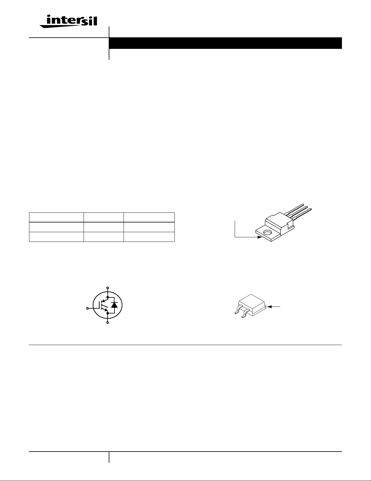
Packaging
JEDEC TO-220AB
E
COLLECTOR
(FLANGE)
C
= 125oC
J
G
Symbol
C
G
G
E
INTERSIL CORPORATION IGBT PRODUCT IS COVERED BY ONE OR MORE OF THE FOLLOWING U.S. PATENTS
4,364,073 4,417,385 4,430,792 4,443,931 4,466,176 4,516,143 4,532,534 4,587,713
4,598,461 4,605,948 4,620,211 4,631,564 4,639,754 4,639,762 4,641,162 4,644,637
4,682,195 4,684,413 4,694,313 4,717,679 4,743,952 4,783,690 4,794,432 4,801,986
4,803,533 4,809,045 4,809,047 4,810,665 4,823,176 4,837,606 4,860,080 4,883,767
4,888,627 4,890,143 4,901,127 4,904,609 4,933,740 4,963,951 4,969,027
TO-263, TO-263AB
COLLECTOR
(FLANGE)
E
1
CAUTION: These devices are sensitive to electrostatic discharge; follow proper ESD Handling Procedures.
1-888-INTERSIL or 321-724-7143
| Copyright © Intersil Corporation 2000
Page 2
HGTP3N60B3D, HGT1S3N60B3DS
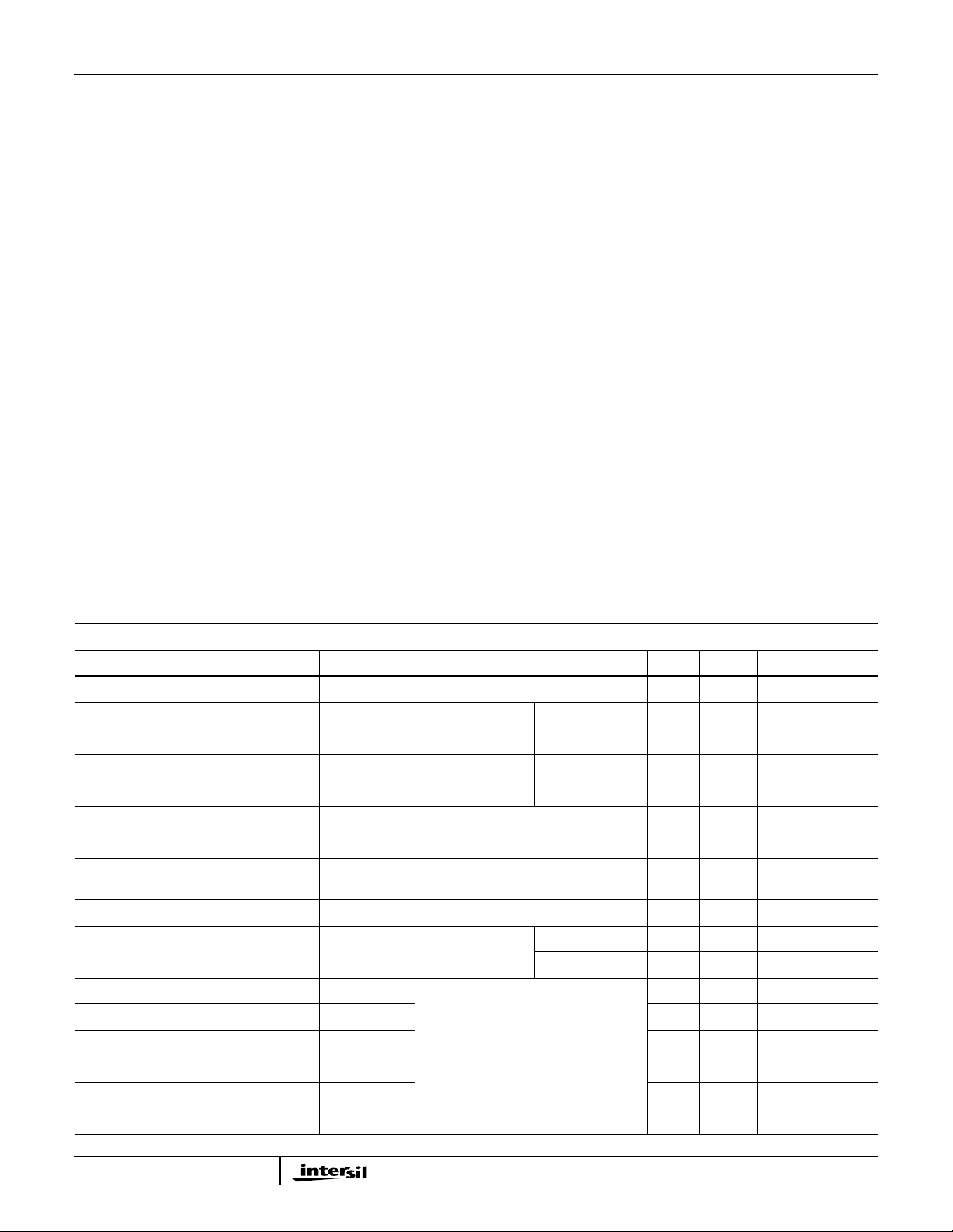
Absolute Maximum Ratings T
= 25oC, Unless Otherwise Specified
C
HGTP3N60B3D,
HGT1S3N60B3DS UNITS
Collector to Emitter Voltage. . . . . . . . . . . . . . . . . . . . . . . . . . . . . . . . . . . . . . . . . . . . . . . . . . . . . . BV
CES
600 V
Collector Current Continuous
At TC = 25oC . . . . . . . . . . . . . . . . . . . . . . . . . . . . . . . . . . . . . . . . . . . . . . . . . . . . . . . . . . . . . . . . . I
At TC = 110oC . . . . . . . . . . . . . . . . . . . . . . . . . . . . . . . . . . . . . . . . . . . . . . . . . . . . . . . . . . . . . . . .I
Average Diode Forward Current . . . . . . . . . . . . . . . . . . . . . . . . . . . . . . . . . . . . . . . . . . . . . . . . .I
EC(AVG)
Collector Current Pulsed (Note 1) . . . . . . . . . . . . . . . . . . . . . . . . . . . . . . . . . . . . . . . . . . . . . . . . . . . . I
Gate to Emitter Voltage Continuous. . . . . . . . . . . . . . . . . . . . . . . . . . . . . . . . . . . . . . . . . . . . . . . . . V
Gate to Emitter Voltage Pulsed . . . . . . . . . . . . . . . . . . . . . . . . . . . . . . . . . . . . . . . . . . . . . . . . . . . . V
C25
C110
CM
GES
GEM
7.0 A
3.5 A
4.0
20 A
±20 V
±30 V
Switching Safe Operating Area at TJ = 150oC (Figure 2) . . . . . . . . . . . . . . . . . . . . . . . . . . . . . . . . SSOA 18A at 600V
Power Dissipation Total at TC = 25oC . . . . . . . . . . . . . . . . . . . . . . . . . . . . . . . . . . . . . . . . . . . . . . . . . .P
D
33.3 W
Power Dissipation Derating TC > 25oC . . . . . . . . . . . . . . . . . . . . . . . . . . . . . . . . . . . . . . . . . . . . . . . . . . . 0.27 W/oC
Operating and Storage Junction Temperature Range . . . . . . . . . . . . . . . . . . . . . . . . . . . . . . . . .TJ, T
STG
-55 to 150
Maximum Lead Temperature for Soldering
Leads at 0.063in (1.6mm) from Case for 10s. . . . . . . . . . . . . . . . . . . . . . . . . . . . . . . . . . . . . . . . . . . T
Package Body for 10s, See Tech Brief 334 . . . . . . . . . . . . . . . . . . . . . . . . . . . . . . . . . . . . . . . . . T
Short Circuit Withstand Time (Note 2) at VGE = 12V. . . . . . . . . . . . . . . . . . . . . . . . . . . . . . . . . . . . . . t
Short Circuit Withstand Time (Note 2) at VGE = 10V. . . . . . . . . . . . . . . . . . . . . . . . . . . . . . . . . . . . . . t
CAUTION: Stresses above those listed in “Absolute Maximum Ratings” may cause permanent damage to the device. This is a stress only rating and operation of the
device at these or any other conditions above those indicated in the operational sections of this specification is not implied.
L
PKG
SC
SC
300
260
5 µs
10 µs
o
C
o
C
o
C
NOTES:
1. Pulse width limited by maximum junction temperature.
2. V
= 360V, TJ = 125oC, RG = 82Ω.
CE(PK)
Electrical Specifications T
= 25oC, Unless Otherwise Specified
C
PARAMETER SYMBOL TEST CONDITIONS MIN TYP MAX UNITS
Collector to Emitter Breakdown Voltage BV
Collector to Emitter Leakage Current I
Collector to Emitter Saturation Voltage V
Gate to Emitter Threshold Voltage V
Gate to Emitter Leakage Current I
CES
CES
CE(SAT)IC
GE(TH)
GES
Switching SOA SSOA T
Gate to Emitter Plateau Voltage V
On-State Gate Charge Q
Current Turn-On Delay Time t
Current Rise Time t
Current Turn-Off Delay Time t
Current Fall Time t
Turn-On Energy E
Turn-Off Energy (Note 1) E
GEP
g(ON)
d(ON)I
rI
d(OFF)I
fI
ON
OFF
IC = 250µA, VGE = 0V 600 - - V
VCE = BV
= I
C110
CES
,
VGE = 15V
IC = 250µA, VCE = V
TC = 25oC - - 250 µA
= 150oC - - 2.0 mA
T
C
TC = 25oC - 1.8 2.1 V
= 150oC - 2.1 2.5 V
T
C
GE
4.5 5.4 6.0 V
VGE = ±20V - - ±250 nA
= 150oC, RG = 82Ω, VGE = 15V
J
18 - - A
L = 500µH, VCE= 600V
IC = I
IC = I
VCE = 0.5 BV
IGBT and Diode at TJ = 25oC
ICE = I
VCE = 0.8 BV
VGE = 15V
RG = 82Ω
L = 1mH
Test Circuit (Figure 19)
, VCE = 0.5 BV
C110
,
C110
C110
CES
- 7.9 - V
VGE = 15V - 18 22 nC
CES
V
= 20V - 21 25 nC
GE
-18- ns
CES
-16- ns
- 105 - ns
-70- ns
-6675µJ
- 88 160 µJ
2
Page 3
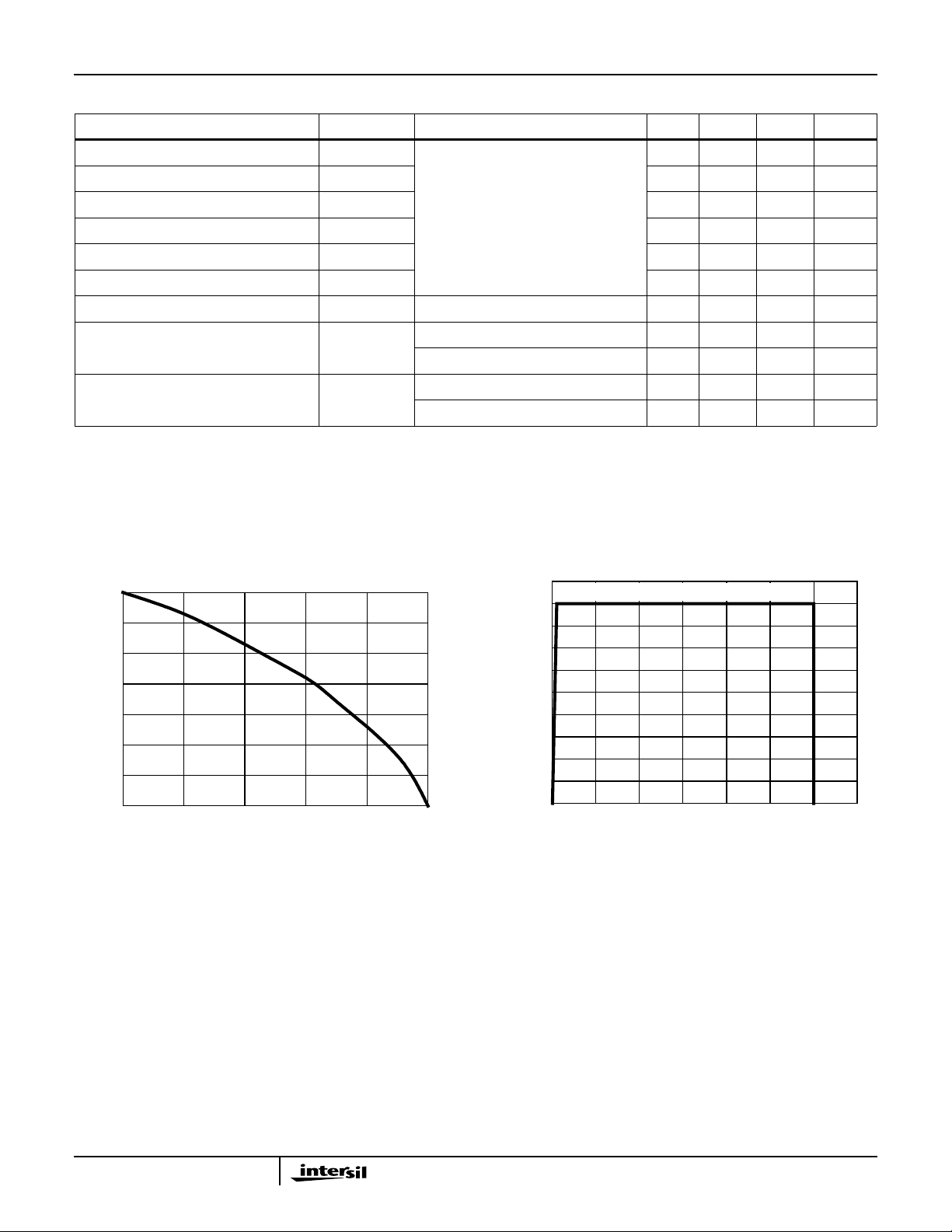
HGTP3N60B3D, HGT1S3N60B3DS
Electrical Specifications T
= 25oC, Unless Otherwise Specified (Continued)
C
PARAMETER SYMBOL TEST CONDITIONS MIN TYP MAX UNITS
Current Turn-On Delay Time t
d(ON)I
Current Rise Time t
Current Turn-Off Delay Time t
d(OFF)I
Current Fall Time t
Turn-On Energy E
Turn-Off Energy (Note 1) E
Diode Forward Voltage V
Diode Reverse Recovery Time t
Thermal Resistance Junction To Case R
rI
fI
ON
OFF
EC
rr
θJC
IGBT and Diode at TJ = 150oC
ICE = I
C110
VCE = 0.8 BV
CES
VGE = 15V
RG = 82Ω
L = 1mH
Test Circuit (Figure 19)
-16- ns
-18- ns
- 220 295 ns
- 115 175 ns
- 130 140 µJ
- 210 325 µJ
IEC = 3A - 2.0 2.5 V
IEC = 1A, dIEC/dt = 200A/µs--22ns
I
= 3A, dIEC/dt = 200A/µs--28ns
EC
IGBT - - 3.75
Diode 3.0
NOTE:
3. Turn-OffEnergy Loss (E
) is definedas theintegral of theinstantaneous powerloss starting atthe trailing edgeof theinput pulse andending
OFF
at the pointwhere the collector current equalszero (ICE= 0A). Alldevices were tested per JEDECStandard No. 24-1 Methodfor Measurement
of Power Device Turn-Off Switching Loss. This test method produces the true total Turn-Off Energy Loss. Turn-On losses include losses due
to diode recovery.
Typical Performance Curves Unless Otherwise Specified
o
o
C/W
C/W
20
7
6
5
4
3
2
, DC COLLECTOR CURRENT (A)
1
CE
I
0
25 50 75 100 125 150
TC, CASE TEMPERATURE (oC)
V
GE
= 15V
TJ= 150oC, RG = 82Ω, VGE= 15V L = 500µH
18
16
14
12
10
8
6
4
2
, COLLECTOR TO EMITTER CURRENT (A)
CE
0
I
0
200
100 500 600
, COLLECTOR TO EMITTER VOLTAGE (V)
V
CE
300 400
700
FIGURE 1. DC COLLECT OR CURRENT vs CASE TEMPERATURE FIGURE 2. MINIMUM SWITCHING SAFE OPERATING AREA
3
Page 4

HGTP3N60B3D, HGT1S3N60B3DS
Typical Performance Curves Unless Otherwise Specified (Continued)
200
100
10
f
MAX1
f
MAX2
= CONDUCTION DISSIPATION
P
, OPERATING FREQUENCY (kHz)
C
MAX
f
R
ØJC
1
1
TJ= 150oC, RG = 82Ω, L = 1mH, VCE= 480V
T
C
o
75
C
o
75
C
o
C
110
110oC
= 0.05 / (t
= (PD- PC) / (EON + E
(DUTY FACTOR = 50%)
= 3.75oC/W, SEE NOTES
246
, COLLECTOR TO EMITTER CURRENT (A)
I
CE
+ t
d(OFF)I
357
d(ON)I
OFF
)
)
V
GE
15V
10V
15V
10V
FIGURE 3. OPERATINGFREQUENCY vsCOLLECTOR TO
EMITTER CURRENT
14
DUTY CYCLE <0.5%, V
PULSE DURATION = 250µs
12
10
8
6
4
2
, COLLECTOR TO EMITTER CURRENT (A)
0
CE
I
012345
, COLLECTOR TO EMITTER VOLTAGE (V)
V
CE
GE
= 10V
T
= 25oC
C
678910
TC = -55oC
TC = 150oC
SC
45
40
35
30
25
20
, PEAK SHORT CIRCUIT CURRENT (A)
SC
I
15
16
VCE = 360V, RG = 82Ω, TJ= 125oC
14
12
10
8
6
, SHORT CIRCUIT WITHSTAND TIME (µs)
4
SC
t
8
10 11 12 13 14 15
VGE, GATE TO EMITTER VOLTAGE (V)
I
t
SC
FIGURE 4. SHORT CIRCUIT WITHSTAND TIME
30
DUTY CYCLE <0.5%, VGE = 15V
PULSE DURATION = 250µs
25
20
15
10
5
, COLLECTOR TO EMITTER CURRENT (A)
0
CE
I
01234
VCE, COLLECTOR TO EMITTER VOLTAGE (V)
TC = 25oC
5678910
TC = -55oC
TC = 150oC
FIGURE 5. COLLECTOR TO EMITTER ON-STATE VOLTAGE FIGURE 6. COLLECTOR TO EMITTER ON-STATE VOLTAGE
0.7
RG = 82Ω, L = 1mH, VCE = 480V
0.6
0.5
0.4
0.3
0.2
, TURN-ON ENERGY LOSS (mJ)
0.1
ON
E
0
, COLLECTOR TO EMITTER CURRENT (A)
I
CE
TJ = 25oC, TJ = 150oC, VGE = 10V
VGE = 15V, TJ = 150oC, TJ = 25oC
7641
FIGURE 7. TURN-ON ENERGYLOSS vs COLLECTORTO
EMITTER CURRENT
8523
0.6
RG = 82Ω, L = 1mH, VCE = 480V
0.5
0.4
0.3
0.2
, TURN-OFF ENERGY LOSS (mJ)
0.1
OFF
E
0
TJ = 150oC; VGE = 10V OR 15V
TJ = 25oC; VGE = 10V OR 15V
3571
ICE, COLLECTOR TO EMITTER CURRENT (A)
FIGURE 8. TURN-OFF ENERGYLOSS vs COLLECTORTO
EMITTER CURRENT
4
8642
Page 5

HGTP3N60B3D, HGT1S3N60B3DS
Typical Performance Curves Unless Otherwise Specified (Continued)
45
RG = 82Ω, L = 1mH, VCE = 480V
40
TJ = 25oC, TJ = 150oC, VGE = 10V
35
30
25
20
, TURN-ON DELAY TIME (ns)
dI
15
t
10
ICE, COLLECTOR TO EMITTER CURRENT (A)
TJ = 25oC, TJ = 150oC, VGE = 15V
42581
763
FIGURE 9. TURN-ON DELAY TIME vs COLLECTOR TO
EMITTER CURRENT
250
225
200
175
150
125
, TURN-OFF DELAY TIME (ns)
100
d(OFF)I
t
75
T
= 25oC, VGE = 15V
J
T
= 25oC, VGE = 10V
J
2
ICE, COLLECTOR TO EMITTER CURRENT (A)
RG = 82Ω, L = 1mH, VCE = 480V
TJ = 150oC, VGE = 15V
T
= 150oC, VGE = 10V
J
4681
753
80
RG = 82Ω, L = 1mH, VCE = 480V
70
60
TJ = 25oC AND TJ = 150oC, VGE= 10V
50
40
, RISE TIME (ns)
rI
t
30
20
10
2
3681
ICE, COLLECTOR TO EMITTER CURRENT (A)
TJ = 25oC, TJ = 150oC, VGE= 15V
FIGURE 10. TURN-ON RISETIME vs COLLECTORTO
EMITTER CURRENT
140
RG = 82Ω, L = 1mH, VCE = 480V
120
TJ = 150oC, VGE = 10V OR 15V
100
, FALL TIME (ns)
fI
t
80
60
24681
ICE, COLLECTOR TO EMITTER CURRENT (A)
TJ = 25oC, VGE = 10V OR 15V
754
753
FIGURE 11. TURN-OFF DELAY TIME vs COLLECTOR TO
EMITTER CURRENT
30
PULSE DURATION = 250µs
25
20
15
10
5
, COLLECTOR TO EMITTER CURRENT (A)
0
CE
I
5789106
V
, GATE TO EMITTER VOLTAGE (V)
GE
TC = -55oC
11 12 13 14 15
= 25oC
T
C
TC = 150oC
FIGURE 13. TRANSFER CHARACTERISTIC FIGURE 14. GATE CHARGE WAVEFORMS
5
FIGURE 12. FALLTIME vs COLLECTORTO EMITTER
CURRENT
15
I
= 1mA,
G(REF)
RL = 171Ω, TC= 25oC
12
9
6
3
, GATE TO EMITTER VOLTAGE (V)
GE
V
0
01051525
VCE = 200V
VCE = 400V VCE = 600V
Qg, GATE CHARGE (nC)
20
Page 6

HGTP3N60B3D, HGT1S3N60B3DS
Typical Performance Curves Unless Otherwise Specified (Continued)
FIGURE 15. CAPACITANCE vs COLLECTOR TO EMITTER VOLTAGE
0
10
0.5
0.2
0.1
-1
10
0.05
0.02
0.01
, NORMALIZED THERMAL RESPONSE
θJC
Z
-2
10
10
SINGLE PULSE
-5
-4
10
500
400
C
IES
300
200
C
C, CAPACITANCE (pF)
100
0
0 5 10 15 20 25
VCE, COLLECTOR TO EMITTER VOLTAGE (V)
-3
10
OES
C
RES
t1, RECTANGULAR PULSE DURATION (s)
FREQUENCY = 1MHz
-2
10
DUTY FACTOR, D = t1 / t
PEAK TJ = (PDX Z
-1
10
θJC
10
P
0
D
X R
t
1
t
2
2
) + T
θJC
C
1
10
FIGURE 16. NORMALIZED TRANSIENT THERMAL RESPONSE, JUNCTION TO CASE
15
12
o
150
9
6
, FORWARD CURRENT (A)
3
EC
I
0
25oC
VEC, FORWARD VOLTAGE (V)
C
o
-55
C
2.0 2.51.51.00.50
FIGURE 17. DIODE FORWARD CURRENT vsFORWARD
VOLTAGE DROP
6
3.0
30
TC = 25oC, dIEC/dt = 200A/µs
25
20
15
10
t, RECOVERY TIMES (ns)
5
0
0.5
14
IEC, FORWARD CURRENT (A)
t
rr
t
a
t
b
23
FIGURE 18. RECOVERY TIME vs FORWARD CURRENT
Page 7

Test Circuit and Waveforms
HGTP3N60B3D, HGT1S3N60B3DS
HGTP3N60B3D
V
GE
V
L = 1mH
RG = 82Ω
FIGURE 19. INDUCTIVE SWITCHING TEST CIRCUIT FIGURE 20. SWITCHING TEST WAVEFORMS
DUT
+
V
= 480V
DD
-
Handling Precautions for IGBTs
Insulated Gate Bipolar Transistors are susceptible to
gate-insulation damage by the electrostatic discharge of
energy through the devices. When handling these de vices ,
care should be exercised to assure that the static charge built
in the handler’s body capacitance is not discharged through
the device. With proper handling and application procedures,
howev er, IGBTs are currently being extensively used in
production by numerous equipment manufacturers in military,
industrial and consumer applications, with virtually no
damage problems due to electrostatic discharge. IGBTs can
be handled safely if the follo wing basic precautions are taken:
1. Prior to assemblyinto a circuit,all leads shouldbe kept
shorted together either by the use of metal shorting
springs or by the insertion into conductive material such
as “ECCOSORBD LD26™” or equivalent.
2. When devicesare removedby hand from their carriers,
the handbeing usedshould begrounded byany suitable
means - for example, with a metallic wristband.
3. Tips of soldering irons should be grounded.
4. Devices shouldnever beinserted into orremoved from
circuits with power on.
5. Gate Voltage Rating -Never exceed the gate-voltage
rating of V
permanent damage to the oxide layer in the gate region.
6. Gate Termination -The gates ofthese devicesare
essentially capacitors. Circuits that leave the gate opencircuited orfloating should be avoided. These conditions
can result in turn-on of the devicedue to voltage buildup
on the input capacitor due to leakage currents or pickup.
7. Gate Protection- These devicesdo nothavean internal
monolithic Zener diode from gate to emitter. If gate
protection is requiredan external Zeneris recommended.
. Exceeding the rated VGE can result in
GEM
CE
90%
I
CE
t
d(OFF)I
10%
t
Operating Frequency Information
Operating frequency information for a typical device
(Figure 3) is presented as a guide for estimating device
performance for a specific application. Other typical
frequency vs collector current (I
the information shownfor a typical unitin Figures5, 6,7, 8, 9
and 11. The operating frequency plot (Figure 3) of a typical
device shows f
point. The information is based on measurements of a
typical device and is bounded by the maximum rated
junction temperature.
f
is defined by f
MAX1
Deadtime (the denominator) hasbeen arbitrarilyheld to10%
of the on-state time for a 50% duty factor. Other definitions
are possible. t
Device turn-off delay can establish an additional frequency
limiting condition for an application other than T
is important when controlling output ripple under a lightly
loaded condition.
f
is defined by f
MAX2
allowable dissipation (P
The sum of device switching and conduction losses must
not exceed P
the conduction losses (P
P
C=VCE
EON and E
x ICE)/2.
OFF
shown in Figure 20. E
power loss (I
integral of the instantaneous power loss (I
turn-off. All tail losses are included in the calculation for
E
; i.e., the collector current equals zero (ICE = 0).
OFF
or f
MAX1
MAX1
and t
d(OFF)I
MAX2
D
. A 50% duty factor was used (Figure 3) and
D
are defined in the switching waveforms
ON
x VCE) during turn-on and E
CE
90%
E
E
OFF
fI
; whichever is smaller at each
MAX2
= 0.05/(t
d(ON)I
ON
) plots are possible using
CE
d(OFF)I
are defined in Figure 20.
= (PD - PC)/(E
) is defined by PD = (TJM - TC)/R
) are approximated by
C
is the integral of the instantaneous
10%
t
rI
t
d(ON)I
+ t
d(ON)I
+ EON). The
OFF
OFF
x VCE) during
CE
. t
JM
is the
).
d(OFF)I
θJC
.
All Intersil semiconductor products are manufactured, assembled and tested under ISO9000 quality systems certification.
Intersil semiconductor products are sold by description only. Intersil Corporation reserves the right to makechanges in circuit design and/or specificationsat any time without notice.Accordingly , the reader is cautioned to verify that data sheets are current before placing orders. Information furnished b y Intersil is believed to be accurate and
reliable. However, no responsibilityis assumed by Intersil or its subsidiaries for its use; nor for anyinfringements of patents or other rights of third parties which may result
from its use. No license is granted by implication or otherwise under any patent or patent rights of Intersil or its subsidiaries.
For information regarding Intersil Corporation and its products, see web site www.intersil.com
7
ECCOSORBD is a Trademark of Emerson and Cumming, Inc.
 Loading...