

Page 1
April 1995
SEMICONDUCTOR
HGTP14N40F3VL
14A, 400V N-Channel,
Logic Level Voltage Clamping IGBT
Features
• Logic Level Gate Drive
• Internal Voltage Clamp
• ESD Gate Protection
•T
= +150oC
J
• Ignition Energy Capable
Applications
• Automotive Ignition
• Small Engine Ignition
• Fuel Ignitor
Description
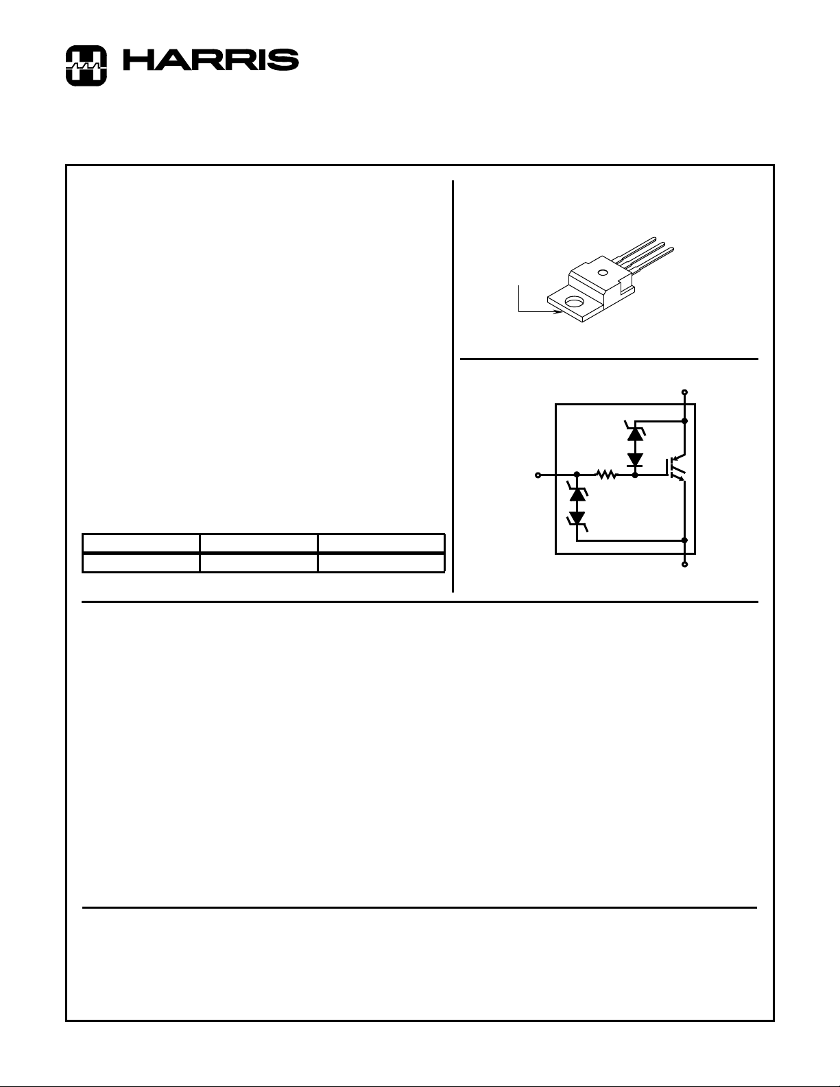
This N-Channel IGBT is a MOS gated, logic level device which is
intended to be used as an ignition coil driver in automotive ignition
circuits. Unique features include an active voltage clamp between
the drain and the gate and ESD protection for the logic level gate.
Some specifications are unique to this automotive application and
are intended to assure device survival in this harsh environment.
The development type number for this device is TA49023.
PACKAGING AVAILABILITY
PART NUMBER PACKAGE BRAND
HGTP14N40F3VL TO-220AB 14N40FVL
NOTE: When ordering, use the entire part number.
Package
COLLECTOR
(FLANGE)
Symbol
GATE
JEDEC TO-220AB
EMITTER
COLLECTOR
EMITTER
COLLECTOR
GATE
Absolute Maximum Ratings T
Collector-Emitter Breakdown Voltage at 10mA . . . . . . . . . . . . . . . . . . . . . . . . . . . . . . . BV
Collector-Gate Breakdown Voltage RGE = 10kΩ . . . . . . . . . . . . . . . . . . . . . . . . . . . . . . BV
Collector Current Continuous
VGE = 4.5V at TC = +25oC . . . . . . . . . . . . . . . . . . . . . . . . . . . . . . . . . . . . . . . . . . . . . . . .I
VGE = 4.5V at TC = +90oC . . . . . . . . . . . . . . . . . . . . . . . . . . . . . . . . . . . . . . . . . . . . . . . .I
Gate-Emitter Voltage Continuous. . . . . . . . . . . . . . . . . . . . . . . . . . . . . . . . . . . . . . . . . . . V
Gate-Emitter Voltage Pulsed or . . . . . . . . . . . . . . . . . . . . . . . . . . . . . . . . . . . . . . . . . . . . V
Gate-Emitter Current Pulsed . . . . . . . . . . . . . . . . . . . . . . . . . . . . . . . . . . . . . . . . . . . . . . . I
Open Secondary Turn-Off Current
L = 2.3mH at +25oC . . . . . . . . . . . . . . . . . . . . . . . . . . . . . . . . . . . . . . . . . . . . . . . . . . . . . I
L = 2.3mH at +150oC . . . . . . . . . . . . . . . . . . . . . . . . . . . . . . . . . . . . . . . . . . . . . . . . . . . . I
Drain to Source Avalanche Energy at L = 2.3mH, TC = +25oC . . . . . . . . . . . . . . . . . . . . . EAS 330 mJ
Power Dissipation Total at TC = +25oC . . . . . . . . . . . . . . . . . . . . . . . . . . . . . . . . . . . . . . . . .P
Power Dissipation Derating TC > +25oC 0.67 W/oC
Operating and Storage Junction Temperature Range . . . . . . . . . . . . . . . . . . . . . . . . .TJ, T
Maximum Lead Temperature for Soldering . . . . . . . . . . . . . . . . . . . . . . . . . . . . . . . . . . . . . .T
Electrostatic Voltage at 100pF, 1500Ω. . . . . . . . . . . . . . . . . . . . . . . . . . . . . . . . . . . . . . . . ESD 6 KV
HARRIS SEMICONDUCTOR IGBT PRODUCT IS COVERED BY ONE OR MORE OF THE FOLLOWING U.S. PATENTS:
4,364,073 4,417,385 4,430,792 4,443,931 4,466,176 4,516,143 4,532,534 4,567,641
4,587,713 4,598,461 4,605,948 4,618,872 4,620,211 4,631,564 4,639,754 4,639,762
4,641,162 4,644,637 4,682,195 4,684,413 4,694,313 4,717,679 4,743,952 4,783,690
4,794,432 4,801,986 4,803,533 4,809,045 4,809,047 4,810,665 4,823,176 4,837,606
4,860,080 4,883,767 4,888,627 4,890,143 4,901,127 4,904,609 4,933,740 4,963,951
4,969,027
= +25oC, Unless Otherwise Specified
C
CES
CGR
C25
C90
GES
GEM
GEM
CO
CO
STG
HGTP14N40F3VL UNITS
420 V
420 V
19
14
±10 V
±12 V
±10 mA
17
12
T
L
83 W
-40 to +150
260
A
A
A
A
o
C
o
C
CAUTION: These devices are sensitive to electrostatic discharge. Users should follow proper ESD Handling Procedures.
Copyright
© Harris Corporation 1995
3-50
File Number 3407.2
Page 2
Specifications HGTP14N40F3VL
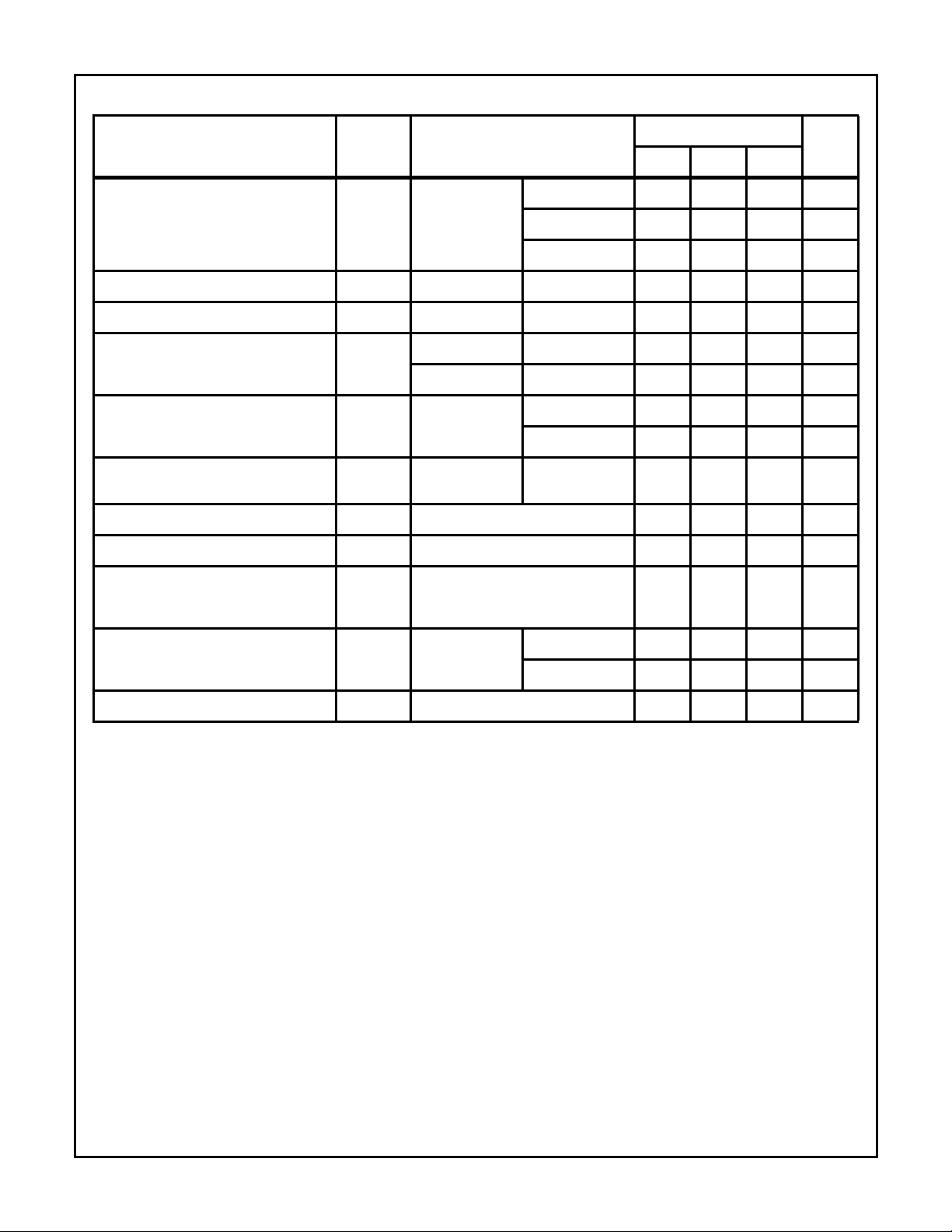
Electrical Specifications T
= +25oC, Unless Otherwise Specified
C
PARAMETERS SYMBOL TEST CONDITIONS
Collector-Emitter Breakdown Voltage BV
Collector-Emitter Clamp Bkdn. Voltage BV
Emitter-Collector Breakdown Voltage BV
Collector-Emitter Leakage Current I
Collector-Emitter Saturation Voltage V
Gate-Emitter Threshold Voltage V
Gate-Emitter Leakage Current I
CES
CE(CL)IC
ECS
CES
CE(SAT)IC
GE(TH)IC
GES
LIMITS
UNITSMIN TYP MAX
IC = 10mA,
TC = +150oC 345 370 415 V
VGE = 0V
TC = +25oC 350 375 420 V
TC = -40oC 355 380 425 V
= 10A TC = +150oC 350 385 430 V
IC = 1.0mA TC = +25oC24--V
VCE = 250V TC = +25oC-- 50µA
V
= 250V TC = +150oC - - 250 µA
CE
= 10A
TC = +25oC - - 2.0 V
VGE = 4.5V
TC = +150oC - - 2.3 V
= 1.0mA
VCE = V
GE
TC = +25oC 1.0 1.5 2.0 V
VGE = ±10V - - ±10 µA
Gate-Emitter Breakdown Voltage BV
Current Turn-off Time-Inductive Load t
D(OFF)I
t
F(OFF)I
GESIGES
+
= ±1.0mA ±12 - - V
RL = 32Ω, IC = 10A, RG = 25Ω,
L = 550µH, VCL = 320V, VGE = 5V,
TC= +125oC
Inductive Use Test UIS L = 2.3mH,
VG = 5V,
Figure 13
Thermal Resistance R
θJC
-1216µs
TC = +150oC12--A
T
= +25oC17--A
C
- 1.5 -
o
C/W
3-51
Page 3
HGTP14N40F3VL
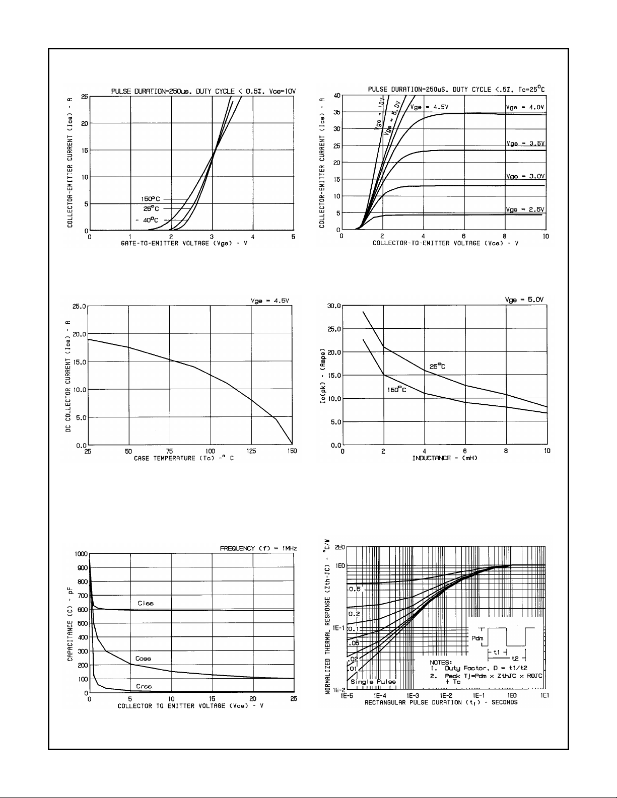
Typical Performance Curves
FIGURE 1. TRANSFER CHARACTERISTICS (TYP.) FIGURE 2. SATURATION CHARACTERISTIC (TYP.)
FIGURE 3. MAXIMUM DC COLLECTOR CURRENT AS A
FUNCTION OF CASE TEMPERATURE
FIGURE 5. CAPACITANCE AS A FUNCTION OF COLLECTOR -
EMITTER VOLTAGE (TYP.)
FIGURE4. OPEN SECONDARY CURRENT AS A FUNCTION OF
INDUCTANCE (TYP.)
FIGURE6. MAXIMUM EFFECTIVE TRANSIENT THERMAL IMPED-
ANCE, JUNCTION-TO-CASE, vs PULSE DURA TION
3-52
Page 4
HGTP14N40F3VL
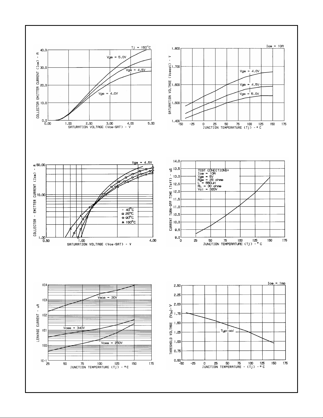
Typical Performance Curves
FIGURE 7. COLLECTOR-EMITTER CURRENT AS A FUNCTION
OF SATURATION VOLTAGE; TJ = +150oC (TYP.)
(Continued)
FIGURE 8. SATURATION VOLTAGE AS A FUNCTION OF
JUNCTION TEMPERATURE (TYP.)
FIGURE 9. COLLECTOR-EMITTER CURRENT AS A FUNCTION
OF SATURATION VOL TAGE (TYP.)
FIGURE 11. LEAKAGE CURRENTS AS A FUNCTION OF
JUNCTION TEMPERATURE (TYP.)
FIGURE 10. INDUCTIVE CURRENT TURN-OFF TIME AS A
FUNCTION OF JUNCTION TEMPERATURE (TYP.)
FIGURE 12. THRESHOLD VOLTAGE AS A FUNCTION OF
JUNCTION TEMPERATURE (TYP.)
3-53
Page 5
Test Circuits
HGTP14N40F3VL
PULSE
GEN
2.3mH
C
R
G
DUT
G
E
V
DD
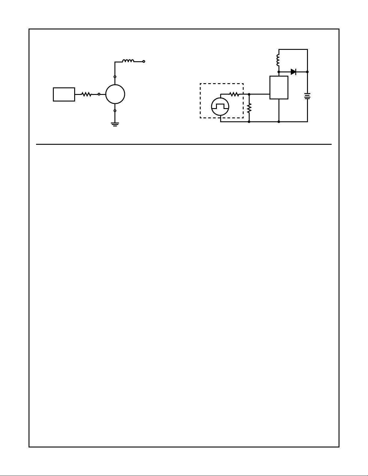
FIGURE 13. USE TEST CIRCUIT FIGURE 14. INDUCTIVE SWITCHING TEST CIRCUIT
Handling Precautions for IGBT’s
Insulated Gate Bipolar Transistors are susceptible to gateinsulation damage by the electrostatic discharge of energy
through the devices. When handling these devices, care
should be exercised to assure that the static charge built in
the handler’s body capacitance is not discharged through
the device. With proper handling and application procedures,
however, IGBT’s are currently being extensively used in
production by numerous equipment manufacturers in
military, industrial and consumer applications, with virtually
no damage problems due to electrostatic discharge. IGBT’s
can be handled safely if the following basic precautions are
taken:
1. Prior to assembly into a circuit, all leads should be kept
shorted together either by the use of metal shorting
springs or by the insertion into conductive material such
as “†ECCOSORBD LD26” or equivalent.
L = 550µH
C
= 1/R
1/R
G
+ 1/R
GEN
R
GEN
5V
= 50Ω
GE
G
R
GE
DUT
= 50Ω
E
+
-
V
CC
320V
2. When devices are removed by hand from their carriers,
the hand being used should be grounded by any suitable
means - for example, with a metallic wristband.
3. Tips of soldering irons should be grounded.
4. Devices should never be inserted into or removed from
circuits with power on.
5. Gate Voltage Rating - Never exceed the gate-voltage
rating of V
. Exceeding the rated VGE can result in per-
GEM
manent damage to the oxide layer in the gate region.
6. Gate Termination - The gates of these devices are
essentially capacitors. Circuits that leave the gate opencircuited or floating should be avoided. These conditions
can result in turn-on of the device due to voltage buildup
on the input capacitor due to leakage currents or pickup.
† Trademark Emerson and Cumming, Inc.
3-54
 Loading...