

Page 1
HGT1S7N60A4S9A, HGTG7N60A4
Data Sheet August 2003
HGTP7N60A4
600V, SMPS Series N-Channel IGBT
The HGT1S7N60A4S9A, HGTG7N6 0A4 and HGTP7N 60A4
are MOS gated high voltage switching devices combining
the best fe atures of MOSFETs and bipolar t ransistors . These
devices have the high input impedance of a MOSFET and
the low on-state conduction loss of a bipolar transistor. The
much lower on-state voltage drop varies only moderately
between 25
This IGBT is ideal for many high voltage switching
applications operating at high frequencies where low
conduction losses are essential. This device has been
optimized for high frequency switch mode power supplies.
Formerly Developmental Type TA49331.
PART NUMBER PACKAGE BRAND
HGT1S7N60A4S9A TO-263AB 7N60A4
HGTG7N60A4 TO-247 7N60A4
HGTP7N60A4 TO-220AB 7N60A4
NOTE: When ordering, use the entire part number.
o
C and 150oC.
Features
• >100kHz Operation at 390V, 7A
• 200kHz Operation at 390V, 5A
• 600V Switching SOA Capability
• Typical Fall Time
. . . . . . . . . . . . . . . . . . . 75ns at T
• Low Conduction Loss
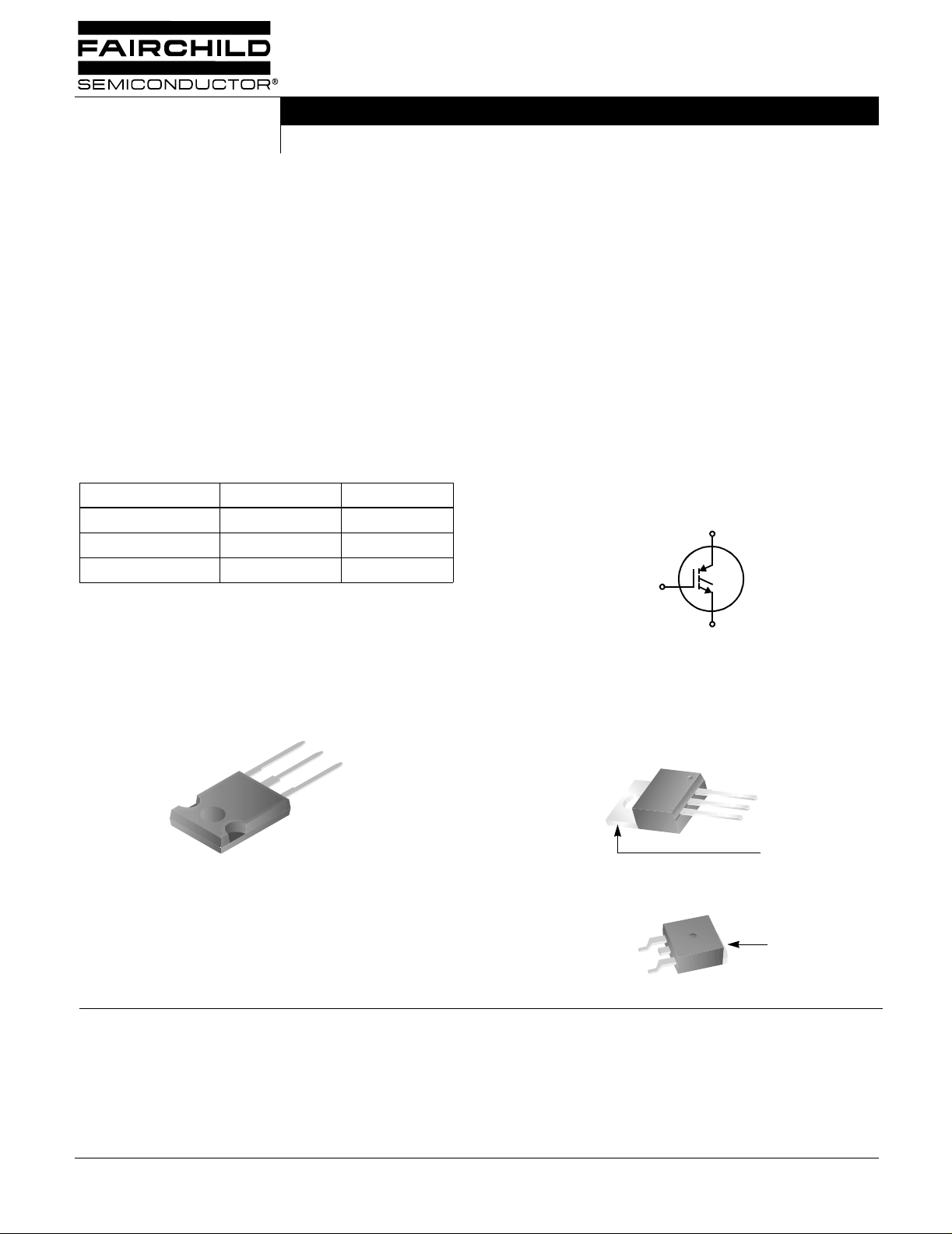
SymbolOrdering Information
G
= 125oC
J
C
E
Packaging
JEDEC STYLE TO-247 JEDEC TO-220AB
E
C
G
E
C
G
COLLECTOR
COLLECTOR
(BOTTOM SIDE METAL)
FAIRCHILD CORPORATION IGBT PRODUCT IS COVERED BY ONE OR MORE OF THE FOLLOWING U.S. PATENTS
4,364,073 4,417,385 4,430,792 4,443,931 4,466,176 4,516,143 4,532,534 4,587,713
4,598,461 4,605,948 4,620,211 4,631,564 4,639,754 4,639,762 4,641,162 4,644,637
4,682,195 4,684,413 4,694,313 4,717,679 4,743,952 4,783,690 4,794,432 4,801,986
4,803,533 4,809,045 4,809,047 4,810,665 4,823,176 4,837,606 4,860,080 4,883,767
4,888,627 4,890,143 4,901,127 4,904,609 4,933,740 4,963,951 4,969,027
JEDEC TO-263AB
G
E
(FLANGE)
COLLECTOR
(FLANGE)
©2003 Fairchild Semiconductor Corporation HGT1S7N60A4S9A, HGTG7N60A4, HGTP7N60A4 Rev. B1
Page 2
HGT1S7N60A4S9A, HGTG7N60A4, HGTP7N60A4
Absolute Maximum Ratings T
= 25oC, Unless Otherwise Specified
C
ALL TYPES UNITS
Collector to Emitter Voltage . . . . . . . . . . . . . . . . . . . . . . . . . . . . . . . . . . . . . . . . . . . . . . . . . BV
CES
600 V
Collector Current Continuous
= 25oC . . . . . . . . . . . . . . . . . . . . . . . . . . . . . . . . . . . . . . . . . . . . . . . . . . . . . . . . . . . . I
At T
C
= 110oC . . . . . . . . . . . . . . . . . . . . . . . . . . . . . . . . . . . . . . . . . . . . . . . . . . . . . . . . . . I
At T
C
Collector Current Pulsed (N o t e 1 ) . . . . . . . . . . . . . . . . . . . . . . . . . . . . . . . . . . . . . . . . . . . . . . .I
Gate to Emitter Voltage Continuous. . . . . . . . . . . . . . . . . . . . . . . . . . . . . . . . . . . . . . . . . . . . V
Gate to Emitter Voltage Pulsed . . . . . . . . . . . . . . . . . . . . . . . . . . . . . . . . . . . . . . . . . . . . . . .V
Switching Safe Operating Area at T
Single Pulse Avalanche Energy at T
Powe r Dissipation Total at T
C
Power Dissipation Derating T
= 150oC, Figure 2 . . . . . . . . . . . . . . . . . . . . . . . . . . . .SSOA 35A at 600V
J
= 25oC. . . . . . . . . . . . . . . . . . . . . . . . . . . . . . . . . . . . . E
C
= 25oC . . . . . . . . . . . . . . . . . . . . . . . . . . . . . . . . . . . . . . . . . . . . P
> 25oC . . . . . . . . . . . . . . . . . . . . . . . . . . . . . . . . . . . . . . . . . . . . . . 1.0 W/oC
C
Operating and Storage Junction Temperature Range . . . . . . . . . . . . . . . . . . . . . . . . . . . T
C25
C110
CM
GES
GEM
AS
D
, T
J
STG
Maximum Lead T emperature for Soldering
Leads at 0.063in (1.6mm) from Case for 10s. . . . . . . . . . . . . . . . . . . . . . . . . . . . . . . . . . . . . .T
Package Body for 10s, See Tech Brief 334 . . . . . . . . . . . . . . . . . . . . . . . . . . . . . . . . . . . . T
CAUTION: Stresses above those listed in “Device M aximum Ratings” m ay cause permanent da mage to the device. This is a stress only rating and operation of th e
device at these or any other conditions above those indicated in the operational sections of this specification is not implied.
L
PKG
34 A
14 A
56 A
±20 V
±30 V
25mJ at 7A
125 W
-55 to 150
300
260
o
C
o
C
o
C
NOTE:
1. Pulse width limited by maximum junction temperature.
Electrical Specifications T
= 25oC, Unless Otherwise Specified
J
PARAMETER SYMBOL TEST CONDITIONS MIN TYP MAX UNITS
Collector to Emitter Breakdown Voltage BV
Emitter to Collector Breakdown Voltage BV
Collector to Emitter Leakage Current I
Collector to Emitter Saturation Voltage V
Gate to Emitter Threshold Voltage V
Gate to Emitter Leakage Current I
CES
ECS
CES
CE(SAT)IC
GE(TH)
GES
Switching SOA SSOA T
Pulsed Avalanche Energy E
Gate to Emitter Plateau Voltage V
On-State Gate Charge Q
Current Turn-On Delay Time t
Current Rise Time t
Current Turn-Off Delay Time t
Current Fall Time t
Turn-On Energy (Note 2) E
Turn-On Energy (Note 2) E
Turn-Off Energy (Note 3) E
AS
GEP
g(ON)
d(ON)I
rI
d(OFF)I
fI
ON1
ON2
OFF
IC = 250µA, VGE = 0V 600 - - V
IC = -10mA, V
= 0V 20 - - V
GE
VCE = 600V TJ = 25oC - - 250 µA
T
= 125oC--2mA
J
= 7A,
V
GE
= 15V
T
= 25oC-1.92.7V
J
T
= 125oC-1.62.2V
J
IC = 250µA, VCE = 600V 4.5 5.9 7.0 V
VGE = ±20V - - ±250 nA
= 150oC, RG = 25Ω, VGE = 15V
J
L = 100µH, V
CE
= 600V
35 - - A
ICE = 7A, L = 500µH25--mJ
IC = 7A, VCE = 300V - 9. 0 - V
IC = 7A,
= 300V
V
CE
IGBT and Diode at TJ = 25oC
I
= 7A
CE
= 390V
V
CE
= 15V
V
GE
R
= 25Ω
G
L = 1mH
Test Circuit (Figure 20)
V
= 15V - 37 45 nC
GE
V
= 20V - 48 60 nC
GE
-11- ns
-11- ns
- 100 - ns
-45- ns
-55- µJ
- 120 150 µJ
-6075µJ
©2003 Fairchild Semiconductor Corporation HGT1S7N60A4S9A, HGTG7N60A4, HGTP7N60A4 Rev. B1
Page 3
HGT1S7N60A4S9A, HGTG7N60A4, HGTP7N60A4
Electrical Specifications T
= 25oC, Unless Otherwise Specified (Continued)
J
PARAMETER SYMBOL TEST CONDITIONS MIN TYP MAX UNITS
Current Turn-On Delay Time t
d(ON)I
Current Rise Time t
Current Turn-Off Delay Time t
d(OFF)I
Current Fall Time t
Turn-On Energy (Note 2) E
Turn-On Energy (Note 2) E
Turn-Off Energy (Note 3) E
Thermal Resistance Junction To Case R
rI
fI
ON1
ON2
OFF
θJC
IGBT and Diode at TJ = 125oC
= 7A
I
CE
= 390V
V
CE
V
= 15V
GE
= 25Ω
R
G
L = 1mH
Test Circuit (Figure 20)
NOTES:
2. Values for two Turn-On loss conditions are shown for the convenience of the circuit designer. E
is the turn-on loss when a typical diode is used in the test circuit and the diode is at the same T
Figure 20.
3. Turn-Off Energy Loss (E
at the point where the collector current equals zero (I
) is defined as the integral of the instantaneous power loss starting at the trailing edge of the input pulse and ending
OFF
= 0A). All devices were tested per JEDEC Standard No. 24-1 Method for Measurement
CE
of Power Device Turn-Off Switching Loss. This test method produces the true total Turn-Off Energy Loss.
Typical Performance Curves Unless Otherwise Specified
35
30
25
V
= 15V
GE
40
TJ = 150oC, RG = 25Ω, V
30
-10- ns
-7-ns
- 130 150 ns
-7585ns
-50- µJ
- 200 215 µJ
- 125 170 µJ
--1.0oC/W
is the turn-on loss of the IGBT only. E
ON1
as the IGBT. The diode type is specified in
J
= 15V, L = 100µH
GE
ON2
20
15
10
, DC COLLECTOR CURRENT (A)
5
CE
I
0
25 75 100 125 150
50
TC, CASE TEMPERATURE (oC)
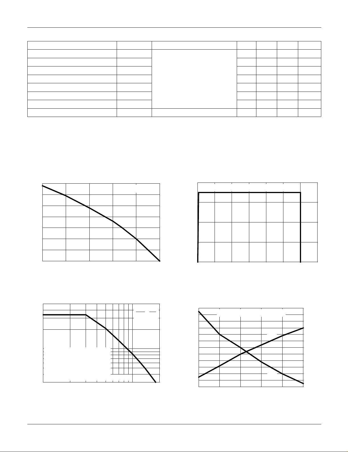
FIGURE 1. DC COLLECTOR CURRENT vs CASE
TEMPERATURE
500
200
100
f
= 0.05 / (t
MAX1
= (PD - PC) / (E
f
MAX2
P
= CONDUCTION DISSIPATION
C
, OPERATING FREQUENCY (kHz)
MAX
f
30
(DUTY FACTOR = 50%)
R
= 1.0oC/W, SEE NOTES
ØJC
TJ = 125oC, RG = 25Ω, L = 2mH, V
1
d(OFF)I
, COLLECTOR TO EMITTER CURRENT (A)
I
CE
ON2
+ t
d(ON)I
+ E
OFF
)
)
= 390V
CE
TCV
o
75
C
15V
FIGURE 3. OPERATING FREQUENCY vs COLLECT OR TO
EMITTER CURRENT
GE
20
10
, COLLECTOR TO EMITTER CURRENT (A)
CE
0
I
0
VCE, COLLECTOR TO EMITTER VOLTAGE (V)
300 400200100 500 600
700
FIGURE 2. MINIMUM SWITCHING SAFE OPERATING AREA
s)
µ
14
12
10
8
6
20510
, SHORT CIRCUIT WITHSTAND TIME (
4
SC
t
10
VCE = 390V, RG = 25Ω, TJ = 125oC
I
SC
t
SC
11 12 15
VGE, GATE TO EMITTER VOLTAGE (V)
13 14
14016
120
100
80
60
40
20
, PEAK SHORT CIRCUIT CURRENT (A )
SC
I
FIGURE 4. SHORT CIRCUIT WITHSTAND TIME
©2003 Fairchild Semiconductor Corporation HGT1S7N60A4S9A, HGTG7N60A4, HGTP7N60A4 Rev. B1
Page 4

HGT1S7N60A4S9A, HGTG7N60A4, HGTP7N60A4
Typical Performance Curves Unless Otherwise Specified (Continued)
30
DUTY CYCLE < 0.5%, V
PULSE DURATION = 250µs
25
20
15
10
5
, COLLECT O R TO EMITTER CURRENT (A)
CE
I
0
01.0
TJ = 150oC
0.5 2.5
, COLLECTOR TO EMITTER VOLTA GE (V)
V
CE
= 12V
GE
TJ = 125oC
TJ = 25oC
1.5 2.0 3.0
30
DUTY CYCLE < 0.5%, VGE = 15V
PULSE DURATION = 250µs
25
20
15
10
5
, COLLECTOR TO EMITTER CURRENT (A)
CE
0
I
0 1.0 1.5 2.0 3.00.5 2.5
VCE, COLLECTOR TO EMITTER VOLTAGE (V)
TJ = 125oC
TJ = 150oC TJ = 25oC
FIGURE 5. COLLECTOR TO EMITTER ON-STATE VOLTAGE FIGURE 6. COLLECTOR TO EMITTER ON-STATE VOLTAGE
500
RG = 25Ω, L = 1mH, VCE = 390V
400
TJ = 125oC, VGE = 12V, VGE = 15V
300
200
, TURN-ON ENERGY LOSS (µJ)
100
ON2
E
0
0
I
, COLLECTOR TO EMITTER CURRENT (A)
CE
TJ = 25oC, VGE = 12V, VGE = 15V
42 6 8 101214
350
RG = 25Ω, L = 1mH, VCE = 390V
300
250
200
TJ = 125oC, VGE = 12V OR 15V
150
100
, TURN-OFF ENERGY LOSS (µJ)
50
OFF
E
0
I
, COLLECTOR TO EMITTER CURRENT (A)
CE
TJ = 25oC, VGE = 12V OR 15V
42 6 8 1012140
FIGURE 7. TURN-ON ENERGY LOSS vs COLLECTOR TO
EMITTER CURRENT
16
RG = 25Ω, L = 1mH, VCE = 390V
TJ = 25oC, VGE = 12V
14
12
10
, TURN-ON DELAY TIME (ns)
d(ON)I
t
8
ICE, COLLECTOR TO EMITTER CURRENT (A)
42681012140
TJ = 125oC, VGE = 12V
TJ = 25oC, VGE = 15V
TJ = 125oC, VGE = 15V
FIGURE 9. TURN-ON DELAY TIME vs COLLECTOR T O
EMITTER CURRENT
©2003 Fairchild Semiconductor Corporation HGT1S7N60A4S9A, HGTG7N60A4, HGTP7N60A4 Rev. B1
FIGURE 8. TURN-OFF ENERGY LOSS vs COLLECTOR T O
EMITTER CURRENT
40
RG = 25Ω, L = 1mH, VCE = 390V
30
20
, RISE TIME (ns)
rI
t
10
0
TJ = 25oC, V
42681012140
ICE, COLLECTOR TO EMITTER CURRENT (A)
= 12V, V
GE
TJ = 125oC, V
GE
= 15V
GE
= 12V, V
GE
= 15V
FIGURE 10. TURN-ON RISE TIME vs COLLECTOR TO
EMITTER CURRENT
Page 5

HGT1S7N60A4S9A, HGTG7N60A4, HGTP7N60A4
Typical Performance Curves Unless Otherwise Specified (Continued)
180
160
140
120
100
, TURN-OFF DELAY TIME (ns)
80
d(OFF)I
t
60
RG = 25Ω, L = 1mH,
42681012140
, COLLECTOR TO EMITTER CURRENT (A)
I
CE
= 390V
V
CE
VGE = 15V, TJ = 125oC
VGE = 12V, TJ = 125oC
VGE = 15V, TJ = 25oC
VGE = 12V, TJ = 25oC
FIGURE 11. TURN-OFF DELA Y TIME vs COLLECT OR T O
EMITTER CURRENT
120
DUTY CYCLE < 0.5%, V
PULSE DURATION = 250µs
100
80
60
40
= 10V
CE
TJ = 25oC
TJ = 125oC TJ = -55oC
90
RG = 25Ω, L = 1mH, VCE = 390V
80
70
60
50
, FALL TIME (ns)
fI
t
40
30
20
ICE, COLLECTOR TO EMITTER CURRENT (A)
TJ = 125oC, VGE = 12V OR 15V
TJ = 25oC, VGE = 12V OR 15V
42 6 8 1012140
FIGURE 12. FALL TIME vs COLL ECT OR T O EMITTER
CURRENT
15
I
= 1mA, RL = 43Ω, TJ = 25oC
G(REF)
12
9
6
VCE = 600V
VCE = 400V
VCE = 200V
20
, COLLECTOR TO EMITTER CURRENT (A)
0
CE
I
7
8 9 11 12 15
, GATE TO EMITTER VOLTAGE (V)
V
GE
1310
FIGURE 13. TRANSFER CHARACTERISTIC FIGURE 14. GATE CHARGE WAVEFORMS
800
RG = 25Ω, L = 1mH, VCE = 390V, VGE = 15V
E
= E
TOTAL
600
400
200
, TOTAL SWITCHING ENERGY LOSS (µJ)
0
TOTAL
E
+ E
ON2
OFF
ICE = 14A
ICE = 7A
ICE = 3.5A
50 75 100
, CASE TEMPERATURE (oC)
T
C
FIGURE 15. TOTAL SWITCHING LOSS vs CASE
TEMPERATURE
14
12525 150
3
, GATE TO EMITTER VOLTAGE (V)
GE
V
0
, TOTAL SWITCHING ENERGY LOSS (mJ)
0.1
TOTAL
E
5101520 3025 35 400
QG, GATE CHARGE (nC)
10
TJ = 125oC, L = 1mH, VCE = 390V, VGE = 15V
E
= E
TOTAL
1
10 1000
+ E
ON2
OFF
ICE = 14A
ICE = 7A
ICE = 3.5A
, GATE RESISTANCE (Ω)
R
G
100
FIGURE 16. TOTAL SWITCHING LOSS vs GATE RESISTANCE
©2003 Fairchild Semiconductor Corporation HGT1S7N60A4S9A, HGTG7N60A4, HGTP7N60A4 Rev. B1
Page 6

HGT1S7N60A4S9A, HGTG7N60A4, HGTP7N60A4
Typical Performance Curves Unless Otherwise Specified (Continued)
1.4
FREQUENCY = 1MHz
1.2
1.0
0.8
0.6
0.4
C, CAPACITANCE (nF)
0.2
0
0 20406080100
C
IES
C
OES
C
RES
VCE, COLLECTOR TO EMITTER VOLTAGE (V)
FIGURE 17. CAPA CITANCE vs COLLECTOR T O EMITTER
VOLTAGE
0
10
0.5
2.8
2.6
2.4
2.2
2.0
, COLLECTOR TO EMITTER VOLTAGE (V)
CE
1.8
V
9
10 12
11 13 14 15 16
VGE, GATE TO EMITTER VOLTAGE (V)
DUTY CYCLE < 0.5%, TJ = 25oC
PULSE DURA TION = 250µs,
ICE = 14A
ICE = 7A
ICE = 3.5A
FIGURE 18. COLLECTOR T O EMITTER ON-STATE V OLTA GE
vs GATE TO EMITTER VOLTAGE
0.2
0.1
-1
10
0.05
0.02
0.01
, NORMALIZED THERMAL RESPONSE
Z
θJC
-2
10
-5
10
SINGLE PULSE
-4
10
FIGURE 19. IGBT NORMALIZED TRANSIENT THERMAL RESPONSE, JUNCTION TO CASE
Test Circuit and Waveforms
RHRP660
L = 1mH
RG = 25Ω
-3
10
t1, RECTANGULAR PULSE DURATION (s)
+
-
VDD = 390V
10
t
1
P
D
t
2
DUTY FACTOR, D = t1 / t
PEAK TJ = (PD X Z
-2
V
GE
V
CE
I
CE
-1
10
90%
t
d(OFF)I
10%
10
90%
E
OFF
t
fI
2
X R
10%
θJC
t
d(ON)I
t
) + T
rI
C
1
10
θJC
0
E
ON2
FIGURE 20. INDUCTIVE SWITCHING TEST CIRCUIT FIGURE 21. SWITCHING TEST WAVEFORMS
©2003 Fairchild Semiconductor Corporation HGT1S7N60A4S9A, HGTG7N60A4, HGTP7N60A4 Rev. B1
Page 7

HGT1S7N60A4S9A, HGTG7N60A4, HGTP7N60A4
Handling Precautions for IGBTs
Insulated Gate Bipolar Transistors are susceptible to
gate-insulation damage by the electrostatic discharge of
energy through the devices. When handling these devices,
care should be exercised to assure that the static charge
built in the handler’s body capacitance is not discharged
through the device. With proper handling and application
procedures, however, IGBTs are currently being ex tensively
used in production b y nume rous equipme nt manuf acturers i n
military, industrial and consumer applications, with virtually
no damage problems due to electrostatic discharge. IGBTs
can be handled safely if the following basic precautions are
taken:
1. Prior to assembly int o a circ uit, al l lead s sho uld be k ept
shorted together either by the use of metal shorting
springs or by the insertion into conductive material such
as “ECCOSORBD LD26” or equivalent.
2. When device s are remov ed b y hand from thei r carriers,
the hand being used should be grounde d b y any su itab le
means - for example, with a metallic wristband.
3. Tips of soldering irons should be grounded.
4. Devices sho uld n e ver be inserted into or removed from
circuits with power on.
5. Gate V olta ge Rating - Nev er e xceed the gate-v oltag e
rating of V
permanent damage to the oxide layer in the gate region.
6. Gate Termin ation - The gates of thes e de vices are
essentially capacitors. Circuits that leave the gate
open-circuited or floating should be avoided. These
conditions can result in turn-on of the device due to
voltage buildup on the input capacitor due to leakage
currents or pickup.
7. Gate Protection - These de vices do no t hav e an internal
monolithic Zener diode from gate to emitter. If gate
protection is required an external Zener is recommended.
. Exceeding the rated VGE can result in
GEM
Operating Frequency Information
Operating frequency information for a typical device
(Figure 3) is presented as a guide for estimating device
performance for a specific application. Other typical
frequency vs collector current (I
the information s hown f or a ty pical un it in Figure s 5, 6, 7, 8, 9
and 11. The operating frequency plot (Figure 3) of a typical
device shows f
MAX1
or f
MAX2
point. The information is based on measurements of a
typical device and is bounded by the maximum rated
junction temperature.
f
is defined by f
MAX1
MAX1
= 0.05/(t
Deadtime (the deno minator) ha s been a rbitra rily held to 10%
of the on-state time for a 50% duty factor. Other definitions
are possible. t
d(OFF)I
and t
d(ON)I
Device turn-off delay can establish an additional frequency
limiting condition for an application other than T
f
is defined by f
MAX2
allowable dissipation (P
= (PD - PC)/(E
MAX2
) is defined by PD = (TJM - TC)/R
D
The sum of device switching and conduction lo sses must
not exceed P
the conduction losse s (P
P
=(VCEx ICE)/2.
C
E
and E
ON2
shown in Figure 21. E
. A 50% duty factor was used (Figure 3) and
D
are defined in the switching waveforms
OFF
) are approximated by
C
is the integral of the
ON2
instantaneous power loss (I
E
is the integral of the instantan eou s power loss
OFF
(I
CExVCE
calculation for E
(I
CE
) during turn-off. All tail losses are incl ude d in the
; i.e., the collector current equals zero
OFF
= 0).
) plots are possible using
CE
; whichever is smaller at each
d(OFF)I
+ t
d(ON)I
).
are defined in Figure 21.
.
JM
+ E
OFF
x VCE) during turn-on and
CE
ON2
). The
θJC
.
©2003 Fairchild Semiconductor Corporation HGT1S7N60A4S9A, HGTG7N60A4, HGTP7N60A4 Rev. B1
Page 8

TRADEMARKS
The following are registered and unregistered trademarks Fairchild Semiconductor owns or is authorized to use and is not
intended to be an exhaustive list of all such trademarks.
ACEx™
ActiveArray™
Bottomless™
CoolFET™
CROSSVOLT™
DOME™
EcoSPARK™
2
CMOS™
E
EnSigna™
FACT™
FACT Quiet Series™
®
FAST
FASTr™
FRFET™
GlobalOptoisolator™
GTO™
HiSeC™
2
C™
I
ImpliedDisconnect™
ISOPLANAR™
Across the board. Around the world.™
The Power Franchise™
Programmable Active Droop™
LittleFET™
MICROCOUPLER™
MicroFET™
MicroPak™
MICROWIRE™
MSX™
MSXPro™
OCX™
OCXPro™
OPTOLOGIC
®
OPTOPLANAR™
PACMAN™
POP™
Power247™
PowerTrench
®
QFET
®
QS™
QT Optoelectronics™
Quiet Series™
RapidConfigure™
RapidConnect™
SILENT SWITCHER
SMART START™
SPM™
Stealth™
SuperSOT™-3
SuperSOT™-6
SuperSOT™-8
SyncFET™
TinyLogic
TINYOPTO™
TruTranslation™
UHC™
UltraFET
®
VCX™
®
®
DISCLAIMER
FAIRCHILD SEMICONDUCTOR RESERVES THE RIGHT TO MAKE CHANGES WITHOUT FURTHER NOTICE TO ANY
PRODUCTS HEREIN TO IMPROVE RELIABILITY, FUNCTION OR DESIGN. FAIRCHILD DOES NOT ASSUME ANY
LIABILITY ARISING OUT OF THE APPLICATION OR USE OF ANY PRODUCT OR CIRCUIT DESCRIBED HEREIN;
NEITHER DOES IT CONVEY ANY LICENSE UNDER ITS PATENT RIGHTS, NOR THE RIGHTS OF OTHERS.
LIFE SUPPORT POLICY
FAIRCHILD’S PRODUCTS ARE NOT AUTHORIZED FOR USE AS CRITICAL COMPONENTS IN LIFE SUPPORT
DEVICES OR SYSTEMS WITHOUT THE EXPRESS WRITTEN APPROVAL OF FAIRCHILD SEMICONDUCTOR
CORPORATION.
As used herein:
1. Life support devices or systems are devices or syst em s
which, (a) are intended for surgical implant into the body,
or (b) support or sustain life, or (c) whose failure to perform
when properly used in accordance with instructions for use
provided in the labeling, can be reasonably expected to
result in significant injury to the user.
2. A critical component is any component of a life support
device or system whose failure to perform can be
reasonably expected to cause the failure of the life support
device or system, or to affect its safety or effectiveness.
PRODUCT STATUS DEFINITIONS
Definition of Terms
Datasheet Identification Product Status Definition
Advance Information Formative or In
Design
Preliminary First Production This datasheet contains preliminary data, and
No Identification Needed Full Production This datasheet contains final specifications. Fairchild
Obsolete Not In Production This datasheet contains specifications on a product
This datasheet contains the design specifications for
product development. Specifications may change in
any manner without notice.
supplementary data will be published at a later date.
Fairchild Semiconductor reserves the right to make
changes at any time without notice in order to improve
design.
Semiconductor reserves the right to make changes at
any time without notice in order to improve design.
that has been discontinued by Fairchild semiconductor.
The datasheet is printed for reference information only.
Rev. I5
 Loading...