

Page 1
HGTP2N120BN, HGTD2N120BNS,
HGT1S2N120BNS
Data Sheet January 2000
12A, 1200V, NPT Series N-Channel IGBT
The HGTP2N120BN, HGTD2N120BNS, and
HGT1S2N120BNS are Non-Punch Through (NPT) IGBT
designs. They are new members of the MOS gated high
voltage switching IGBT family. IGBTs combine the best
features of MOSFETs and bipolar transistors. This device
has the high input impedance of a MOSFET and the low
on-state conduction loss of a bipolar transistor.
The IGBT is ideal for many high voltage switching
applications operating at moderate frequencies where low
conduction losses are essential, such as: AC and DC motor
controls, power supplies and drivers for solenoids, relays
and contactors.
Formerly Developmental Type TA49312.
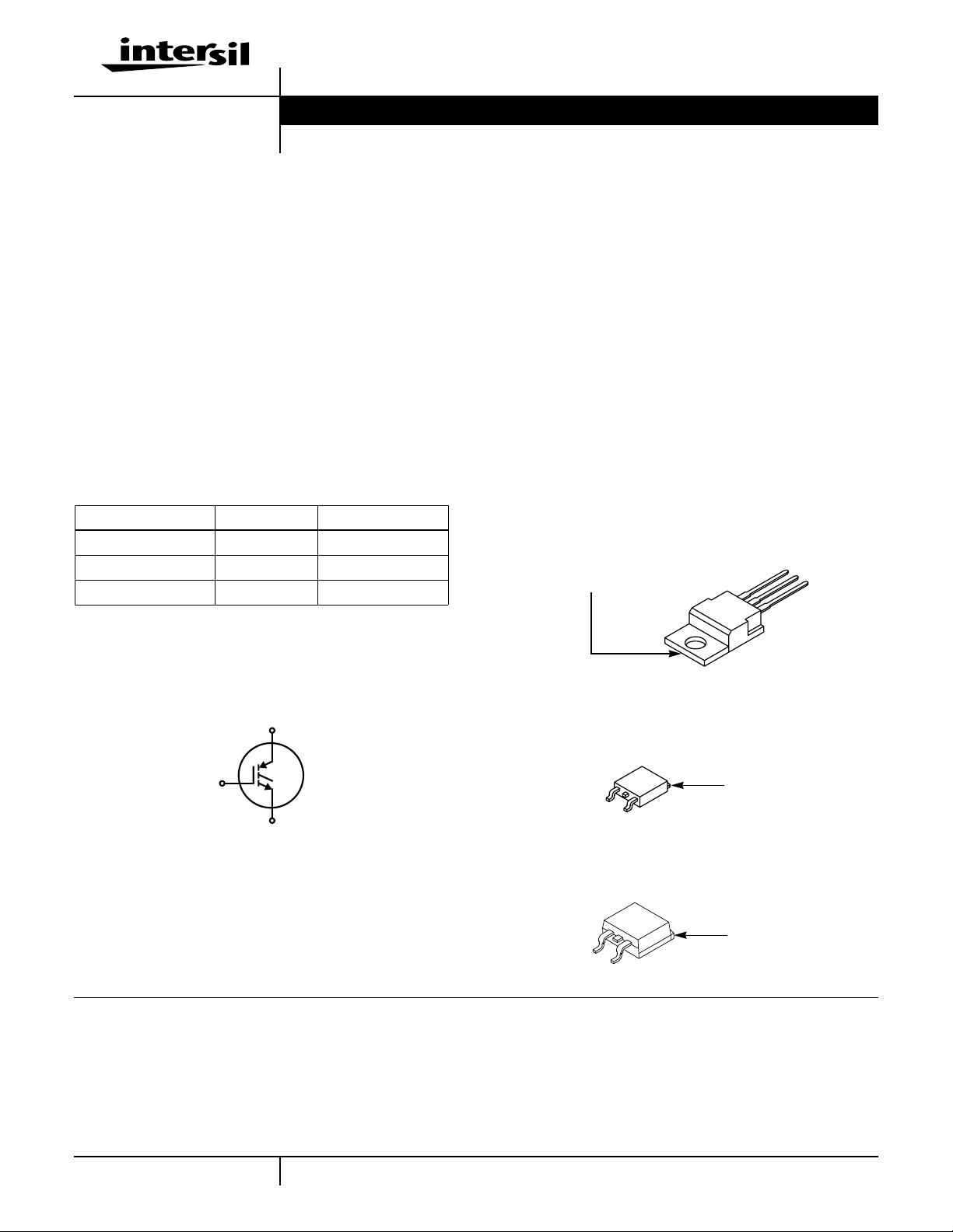
Ordering Information
PART NUMBER PACKAGE BRAND
HGTP2N120BN TO-220AB 2N120BN
HGTD2N120BNS TO-252AA 2N120BN
HGT1S2N120BNS TO-263AB 2N120BN
NOTE: When ordering,use theentirepart number. Addthesuffix 9A
to obtain the TO-263AB and TO-252AA variant in Tape and Reel,
e.g., HGT1S2N120BNS9A.
File Number 4696.2
Features
• 12A, 1200V, TC = 25oC
• 1200V Switching SOA Capability
• Typical Fall Time. . . . . . . . . . . . . . . . 160ns at T
• Short Circuit Rating
• Low Conduction Loss
• Avalanche Rated
• Thermal Impedance SPICE Model
Temperature Compensating SABER™ Model
www.intersil.com
• Related Literature
- TB334 “Guidelines for Soldering Surface Mount
Components to PC Boards”
Packaging
JEDEC TO-220AB
COLLECTOR
(FLANGE)
E
= 150oC
J
C
G
Symbol
C
JEDEC TO-252AA
G
G
E
E
JEDEC TO-263AB
G
E
INTERSIL CORPORATION IGBT PRODUCT IS COVERED BY ONE OR MORE OF THE FOLLOWING U.S. PATENTS
4,364,073 4,417,385 4,430,792 4,443,931 4,466,176 4,516,143 4,532,534 4,587,713
4,598,461 4,605,948 4,620,211 4,631,564 4,639,754 4,639,762 4,641,162 4,644,637
4,682,195 4,684,413 4,694,313 4,717,679 4,743,952 4,783,690 4,794,432 4,801,986
4,803,533 4,809,045 4,809,047 4,810,665 4,823,176 4,837,606 4,860,080 4,883,767
4,888,627 4,890,143 4,901,127 4,904,609 4,933,740 4,963,951 4,969,027
COLLECTOR
(FLANGE)
COLLECTOR
(FLANGE)
1
CAUTION: These devices are sensitive to electrostatic discharge; follow proper ESD Handling Procedures.
1-888-INTERSIL or 321-724-7143
| Copyright © Intersil Corporation 2000
SABER™ is a trademark of Analogy, Inc.
Page 2
HGTP2N120BN, HGTD2N120BNS, HGT1S120BNS
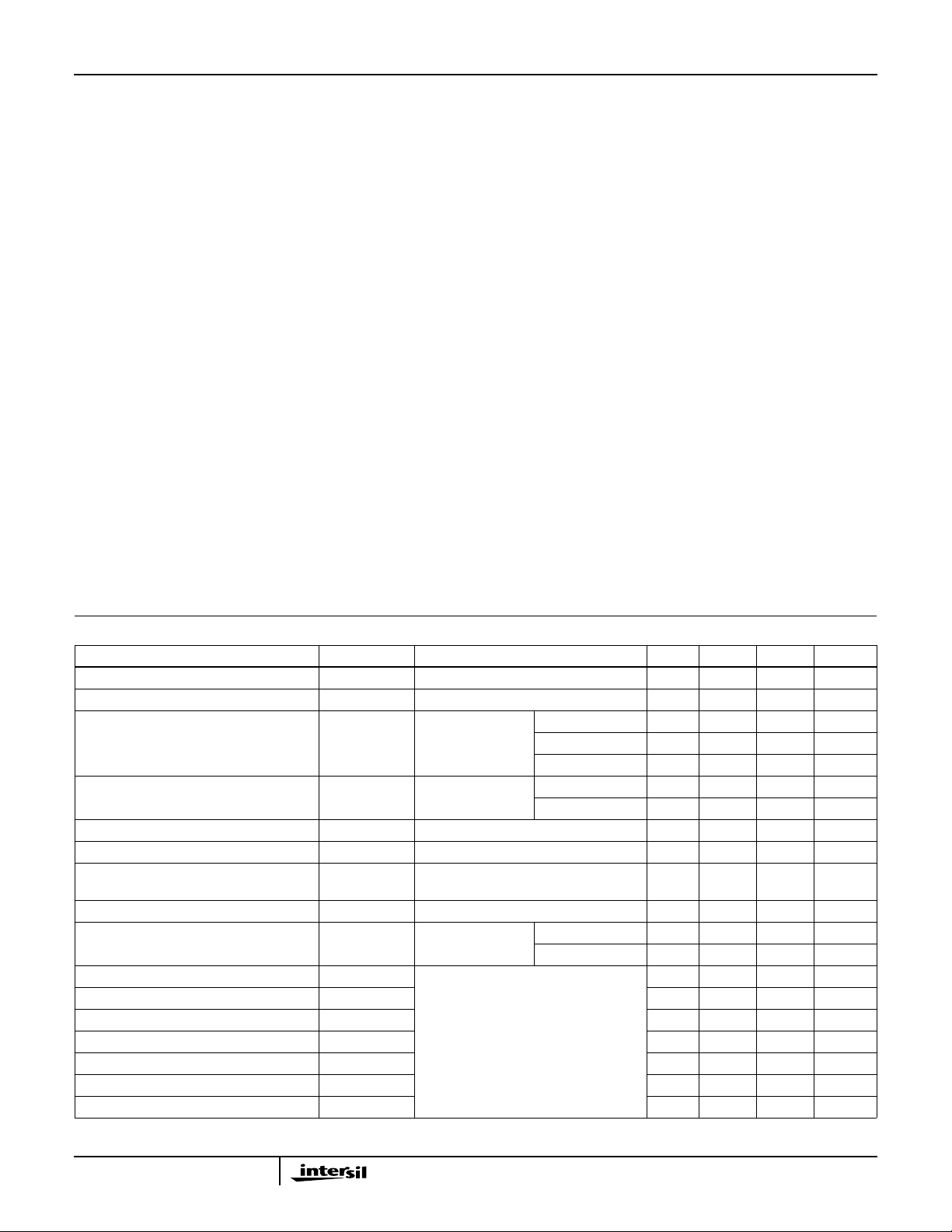
Absolute Maximum Ratings T
= 25oC, Unless Otherwise Specified
C
HGTP2N120BN,
HGTD2N120BNS
HGT1S2N120BNS UNITS
Collector to Emitter Voltage. . . . . . . . . . . . . . . . . . . . . . . . . . . . . . . . . . . . . . . . . . . . . .BV
CES
1200 V
Collector Current Continuous
At TC = 25oC . . . . . . . . . . . . . . . . . . . . . . . . . . . . . . . . . . . . . . . . . . . . . . . . . . . . . . . . .I
At TC = 110oC . . . . . . . . . . . . . . . . . . . . . . . . . . . . . . . . . . . . . . . . . . . . . . . . . . . . . . . I
Collector Current Pulsed (Note 1) . . . . . . . . . . . . . . . . . . . . . . . . . . . . . . . . . . . . . . . . . . . I
Gate to Emitter Voltage Continuous. . . . . . . . . . . . . . . . . . . . . . . . . . . . . . . . . . . . . . . . .V
Gate to Emitter Voltage Pulsed . . . . . . . . . . . . . . . . . . . . . . . . . . . . . . . . . . . . . . . . . . . V
C25
C110
CM
GES
GEM
12 A
5.6 A
20 A
±20 V
±30 V
Switching Safe Operating Area at TJ = 150oC (Figure 2) . . . . . . . . . . . . . . . . . . . . . . . SSOA 12A at 1200V
Power Dissipation Total at TC = 25oC . . . . . . . . . . . . . . . . . . . . . . . . . . . . . . . . . . . . . . . . . P
D
104 W
Power Dissipation Derating TC > 25oC . . . . . . . . . . . . . . . . . . . . . . . . . . . . . . . . . . . . . . . . . . 0.83 W/oC
Forward Voltage Avalanche Energy (Note 2). . . . . . . . . . . . . . . . . . . . . . . . . . . . . . . . . . . E
Operating and Storage Junction Temperature Range . . . . . . . . . . . . . . . . . . . . . . . . TJ, T
AV
STG
18 mJ
-55 to 150
o
C
Maximum Lead Temperature for Soldering
Leads at 0.063in (1.6mm) from case for 10s. . . . . . . . . . . . . . . . . . . . . . . . . . . . . . . . . . T
Package Body for 10s, see Tech Brief 334 . . . . . . . . . . . . . . . . . . . . . . . . . . . . . . . . . .T
Short Circuit Withstand Time (Note 3) at VGE = 15V. . . . . . . . . . . . . . . . . . . . . . . . . . . . . .t
Short Circuit Withstand Time (Note 3) at VGE = 12V. . . . . . . . . . . . . . . . . . . . . . . . . . . . . .t
CAUTION: Stresses above those listed in “Absolute Maximum Ratings” may cause permanent damage to the device. This is a stress only rating and operation of the
device at these or any other conditions above those indicated in the operational sections of this specification is not implied.
L
pkg
SC
SC
300
260
8 µs
15 µs
o
C
o
C
NOTES:
1. Pulse width limited by maximum junction temperature.
2. ICE= 3A, L = 4mH, TJ = 25oC.
3. V
= 840V, TJ = 125oC, RG = 51Ω.
CE(PK)
Electrical Specifications T
= 25oC, Unless Otherwise Specified
C
PARAMETER SYMBOL TEST CONDITIONS MIN TYP MAX UNITS
Collector to Emitter Breakdown Voltage BV
Emitter to Collector Breakdown Voltage BV
Collector to Emitter Leakage Current I
CES
ECS
CES
IC = 250µA, VGE = 0V 1200 - - V
IC = 10mA, VGE= 0V 15 - - V
VCE = BV
CES
TC = 25oC - - 250 µA
TC = 125oC - 40 - µA
TC = 150oC - - 0.5 mA
Collector to Emitter Saturation Voltage V
Gate to Emitter Threshold Voltage V
Gate to Emitter Leakage Current I
CE(SAT)IC
GE(TH)
GES
= 2.3A,
VGE = 15V
IC = 20µA, VCE = V
TC = 25oC - 2.45 2.7 V
TC = 150oC - 3.6 4.2 V
GE
VGE = ±20V - - ±250 nA
Switching SOA SSOA TJ = 150oC, RG = 51Ω, VGE = 15V,
Gate to Emitter Plateau Voltage V
On-State Gate Charge Q
Current Turn-On Delay Time t
d(ON)I
Current Rise Time t
Current Turn-Off Delay Time t
d(OFF)I
Current Fall Time t
Turn-On Energy (Note 4) E
Turn-On Energy (Note 4) E
Turn-Off Energy (Note 5) E
GEP
G(ON)
rI
fI
ON1
ON2
OFF
L = 400µH, V
IC = 2.3A, VCE = 0.5 BV
IC = 2.3A,
VCE = 0.5 BV
IGBT and Diode at TJ = 25oC
ICE = 2.3A
VCE = 0.8 BV
VGE = 15V
RG = 51Ω
L = 5mH
Test Circuit (Figure 18)
CE(PK)
CES
CES
= 1200V
CES
VGE = 15V - 24 30 nC
VGE = 20V - 32 39 nC
6.0 6.8 - V
12 - - A
- 10.2 - V
-2125ns
-1115ns
- 185 240 ns
- 100 130 ns
-83- µJ
- 370 500 µJ
- 195 270 µJ
2
Page 3
HGTP2N120BN, HGTD2N120BNS, HGT1S120BNS
Electrical Specifications T
= 25oC, Unless Otherwise Specified (Continued)
C
PARAMETER SYMBOL TEST CONDITIONS MIN TYP MAX UNITS
Current Turn-On Delay Time t
d(ON)I
Current Rise Time t
Current Turn-Off Delay Time t
d(OFF)I
Current Fall Time t
Turn-On Energy (Note 4) E
Turn-On Energy (Note 4) E
Turn-Off Energy (Note 5) E
Thermal Resistance Junction To Case R
rI
fI
ON1
ON2
OFF
θJC
IGBT and Diode at TJ = 150oC
ICE = 2.3A
VCE = 0.8 BV
CES
VGE = 15V
RG= 51Ω
L = 5mH
Test Circuit (Figure 18)
-2530ns
-1115ns
- 195 260 ns
- 160 200 ns
-83- µJ
- 725 1000 µJ
- 280 380 µJ
- - 1.2
NOTES:
4. Valuesfor two Turn-On loss conditions are shown forthe convenience of the circuit designer.E
is the turn-on loss of the IGBT only. E
ON1
ON2
turn-on loss when a typical diode is used in the test circuit and the diode is at the same TJ as the IGBT. The diode type is specified in Figure 18.
5. Turn-OffEnergy Loss (E
) is defined as the integral ofthe instantaneous powerloss starting atthe trailing edgeof the input pulse and ending
OFF
at the point where the collector current equalszero (ICE= 0A). All devices were tested per JEDEC Standard No. 24-1 Method for Measurement
of Power Device Turn-Off Switching Loss. This test method produces the true total Turn-Off Energy Loss.
Typical Performance Curves Unless Otherwise Specified
12
V
10
8
6
4
, DC COLLECTOR CURRENT (A)
2
CE
I
0
25 75 100 125 150
50
TC, CASE TEMPERATURE (oC)
GE
= 15V
14
TJ= 150oC, RG = 51Ω, VGE= 15V, L = 1mH
12
10
8
6
4
2
, COLLECTOR TO EMITTER CURRENT (A)
CE
I
0
0
VCE, COLLECTOR TO EMITTER VOLTAGE (V)
600 800400200 1000 1200
o
C/W
is the
1400
FIGURE 1. DC COLLECTOR CURRENT vs CASE
TEMPERATURE
TJ= 150oC, RG = 51Ω, L = 5mH, VCE= 960V
100
50
f
MAX1
f
MAX2
, OPERATING FREQUENCY (kHz)
P
MAX
f
R
10
0.5
TC = 75oC, VGE = 15V, IDEAL DIODE
= 0.05 / (t
= (PD- PC) / (E
= CONDUCTION DISSIPATION
C
(DUTY FACTOR = 50%)
= 1.2oC/W, SEE NOTES
ØJC
ICE, COLLECTOR TO EMITTER CURRENT (A)
d(OFF)I
1.0
ON2
+ t
d(ON)I
+ E
OFF
)
)
110oC
110
T
C
o
C
V
15V
12V
GE
T
V
C
o
15V
C
75
o
12V
75
C
FIGURE 3. OPERATINGFREQUENCY vs COLLECTOR TO
EMITTER CURRENT
3
GE
FIGURE 2. MINIMUM SWITCHING SAFE OPERATING AREA
25
VCE = 840V, RG = 51Ω, TJ= 125oC
20
15
10
, SHORT CIRCUIT WITHSTAND TIME (µs)
5
SC
t
5.02.0
12 13 14 15
VGE, GATE TO EMITTER VOLTAGE (V)
t
SC I
SC
40
35
30
25
, PEAK SHORT CIRCUIT CURRENT (A)
SC
I
20
FIGURE 4. SHORT CIRCUIT WITHSTAND TIME
Page 4

HGTP2N120BN, HGTD2N120BNS, HGT1S120BNS
Typical Performance Curves Unless Otherwise Specified (Continued)
10
8
6
4
2
, COLLECTOR TO EMITTER CURRENT (A)
CE
0
I
01 3
TC = -55oC
24
, COLLECTOR TO EMITTER VOLTAGE (V)
V
CE
TC = 25oC
TC = 150oC
DUTY CYCLE < 0.5%, V
250µs PULSE TEST
567
GE
= 12V
10
TC = -55oC
8
6
4
2
DUTY CYCLE < 0.5%, VGE = 15V
, COLLECTOR TO EMITTER CURRENT (A)
0
CE
I
01234 7
VCE, COLLECTOR TO EMITTER VOLTAGE (V)
250
TC = 25oC
µ
s PULSE TEST
TC = 150oC
56
FIGURE 5. COLLECTOR TO EMITTER ON-STATE VOLTAGE FIGURE 6. COLLECTOR TO EMITTER ON-STATE VOLTAGE
2.0
RG = 51Ω, L = 5mH, VCE = 960V
1.5
TJ = 150oC, VGE = 12V, VGE = 15V
1.0
0.5
, TURN-ON ENERGY LOSS (mJ)
ON2
E
0
10
, COLLECTOR TO EMITTER CURRENT (A)
I
CE
TJ = 25oC, VGE = 12V, VGE = 15V
2
3
45
400
RG = 51Ω, L = 5mH, VCE = 960V
350
300
TJ = 150oC, VGE = 12V OR 15V
250
200
150
100
, TURN-OFF ENERGY LOSS (mJ)
50
OFF
E
0
10
I
, COLLECTOR TO EMITTER CURRENT (A)
CE
2
TJ = 25oC, VGE = 12V OR 15V
3
45
FIGURE 7. TURN-ON ENERGY LOSS vs COLLECTORTO
EMITTER CURRENT
45
RG = 51Ω, L = 5mH, VCE = 960V
40
TJ = 25oC, TJ = 150oC, VGE = 12V
35
30
25
, TURN-ON DELAY TIME (ns)
20
dI
t
15
0
1
I
, COLLECTOR TO EMITTER CURRENT (A)
CE
TJ = 25oC, TJ = 150oC, VGE = 15V
2
3
45
FIGURE 9. TURN-ON DELAY TIME vs COLLECTORTO
EMITTER CURRENT
4
FIGURE 8. TURN-OFF ENERGY LOSS vs COLLECTORTO
EMITTER CURRENT
40
RG = 51Ω, L = 5mH, VCE = 960V
35
TJ = 25oC, TJ = 150oC, VGE= 12V
TJ = 25oC OR TJ = 150oC, VGE= 15V
2
ICE, COLLECTOR TO EMITTER CURRENT (A)
40315
, RISE TIME (ns)
rI
t
30
25
20
15
10
5
0
FIGURE 10. TURN-ON RISE TIME vs COLLECTORTO
EMITTER CURRENT
Page 5

HGTP2N120BN, HGTD2N120BNS, HGT1S120BNS
Typical Performance Curves Unless Otherwise Specified (Continued)
450
400
350
300
250
200
, TURN-OFF DELAY TIME (ns)
150
d(OFF)I
t
100
VGE = 12V, VGE = 15V, TJ = 25oC
0
1
, COLLECTOR TO EMITTER CURRENT (A)
I
CE
RG = 51Ω, L = 5mH, VCE = 960V
VGE = 12V, VGE = 15V, TJ = 150oC
2
4
FIGURE 11. TURN-OFF DELAY TIME vs COLLECTORTO
EMITTER CURRENT
30
DUTY CYCLE < 0.5%, V
250µs PULSE TEST
25
20
CE
= 20V
400
RG = 51Ω, L = 5mH, VCE = 960V
350
300
250
200
, FALL TIME (ns)
fI
t
150
100
TJ = 25oC, VGE = 12V OR 15V
50
53
0
ICE, COLLECTOR TO EMITTER CURRENT (A)
TJ = 150oC, VGE = 12V OR 15V
1
2
543
FIGURE 12. FALLTIME vs COLLECTORTO EMITTER
CURRENT
20
I
= 1mA, RL = 260Ω, TC = 25oC
G(REF)
15
VCE = 1200V
15
10
5
0
7
TC = 150oC
VGE, GATE TO EMITTER VOLTAGE (V)
, COLLECTOR TO EMITTER CURRENT (A)
CE
I
TC = 25oC
TC = -55oC
11
14 15
138 9 10 12
10
VCE = 400V
5
, GATE TO EMITTER VOLTAGE (V)
GE
V
0
020525
QG, GATE CHARGE (nC)
VCE = 800V
FIGURE 13. TRANSFER CHARACTERISTIC FIGURE 14. GATE CHARGE WAVEFORMS
0.8
FREQUENCY = 1MHz
0.6
C
IES
0.4
C, CAPACITANCE (nF)
0.2
C
RES
0
0 5 10 15 20 25
C
OES
VCE, COLLECTOR TO EMITTER VOLTAGE (V)
3.0
DUTY CYCLE < 0.5%, TC = 110oC
250µs PULSE TEST
2.5
2.0
1.5
1.0
0.5
, COLLECTOR TO EMITTER CURRENT (A)
CE
0
I
0 1.0
0.5 1.5 2.5 3.5
VCE, COLLECTOR TO EMITTER VOLTAGE (V)
VGE = 15V
2.0
3010 15
VGE = 10V
3.0 4.0
35
FIGURE 15. CAPACITANCE vs COLLECTOR TO EMITTER
VOLTAGE
5
FIGURE 16. COLLECTOR TO EMITTER ON-STATE VOLTAGE
Page 6

HGTP2N120BN, HGTD2N120BNS, HGT1S120BNS
Typical Performance Curves Unless Otherwise Specified (Continued)
0
10
0.5
0.2
0.1
-1
10
0.05
0.02
JC
θ
0.01
-5
SINGLE PULSE
-4
10
-2
10
10
, NORMALIZED THERMAL RESPONSE
Z
DUTY FACTOR, D = t1 / t
PEAK TJ = (PDX Z
-3
10
t
, RECTANGULAR PULSE DURATION (s)
1
θJC
2
X R
10
FIGURE 17. NORMALIZED TRANSIENT THERMAL RESPONSE, JUNCTION TO CASE
Test Circuit and Waveforms
θJC
t
1
P
) + T
C
-2
D
t
2
-1
10
0
10
HGTP2N120BND
90%
E
ON2
10%
t
d(ON)I
t
rI
RG = 51Ω
L = 5mH
V
GE
E
V
CE
90%
+
= 960V
V
DD
-
I
CE
t
d(OFF)I
10%
OFF
t
fI
FIGURE 18. INDUCTIVE SWITCHING TEST CIRCUIT FIGURE 19. SWITCHING TEST WAVEFORMS
6
Page 7

HGTP2N120BN, HGTD2N120BNS, HGT1S120BNS
Handling Precautions for IGBTs
Insulated Gate Bipolar Transistors are susceptible to
gate-insulation damage by the electrostatic discharge of
energy through the devices. When handling these devices,
care should be exercised to assure that the static charge
built in the handler’s body capacitance is not discharged
through the device. With proper handling and application
procedures, however, IGBTs are currently being extensively
used in production by numerousequipment manufacturersin
military, industrial and consumer applications, with virtually
no damage problems due to electrostatic discharge. IGBTs
can be handled safely if the following basic precautions are
taken:
1. Prior to assembly into a circuit, all leads should be kept
shorted together either by the use of metal shorting
springs or by the insertion into conductive material such
as “ECCOSORBD™ LD26” or equivalent.
2. When devices are removed by hand from their carriers,
the hand being used should be groundedby anysuitable
means - for example, with a metallic wristband.
3. Tips of soldering irons should be grounded.
4. Devices should never be inserted into or removed from
circuits with power on.
5. Gate Voltage Rating - Never exceedthe gate-voltage
rating of V
permanent damage to the oxide layer in the gate region.
6. Gate Termination- The gatesof these devicesare
essentially capacitors. Circuits that leave the gate
open-circuited or floating should be avoided. These
conditions can result in turn-on of the device due to
voltage buildup on the input capacitor due to leakage
currents or pickup.
7. Gate Protection- Thesedevices do not have an internal
monolithic Zener diode from gate to emitter. If gate
protection is requiredan external Zener is recommended.
. Exceeding the rated VGE can result in
GEM
Operating Frequency Information
Operating frequency information for a typical device
(Figure 3) is presented as a guide for estimating device
performance for a specific application. Other typical
frequency vs collector current (I
the information shown fora typicalunit in Figures 5, 6, 7, 8, 9
and 11. The operating frequency plot (Figure 3) of a typical
device shows f
MAX1
or f
MAX2
point. The information is based on measurements of a
typical device and is bounded by the maximum rated
junction temperature.
f
is defined by f
MAX1
MAX1
= 0.05/(t
Deadtime (the denominator) hasbeen arbitrarily held to 10%
of the on-state time for a 50% duty factor. Other definitions
are possible. t
d(OFF)I
and t
d(ON)I
Device turn-off delay can establish an additional frequency
limiting condition for an application other than T
is important when controlling output ripple under a lightly
loaded condition.
f
is defined by f
MAX2
allowabledissipation (P
= (PD - PC)/(E
MAX2
) is defined by PD=(TJM-TC)/R
D
The sum of device switching and conduction losses must
not exceed P
the conduction losses (P
P
=(VCExICE)/2.
C
E
and E
ON2
shown in Figure 19. E
. A 50% duty factor was used (Figure 3) and
D
are defined in the switching waveforms
OFF
) are approximated by
C
is the integral of the
ON2
instantaneous power loss (I
E
is the integral of the instantaneous power loss
OFF
(I
CExVCE
calculation for E
(I
CE
) during turn-off. All tail losses are included in the
; i.e., the collector current equals zero
OFF
= 0).
) plots are possible using
CE
; whichever is smaller at each
d(OFF)I
+ t
d(ON)I
).
are defined in Figure 19.
. t
JM
d(OFF)I
+ E
OFF
x VCE) during turn-on and
CE
ON2
). The
θJC
.
All Intersil semiconductor products are manufactured, assembled and tested under ISO9000 quality systems certification.
Intersil semiconductor products are sold by description only. Intersil Corporation reserves the right to make changes in circuit design and/or specifications at any time without notice. Accordingly, the reader is cautioned to verify that data sheets are current before placing orders. Information furnished by Intersil is believed to be accurate and
reliable. However,no responsibility is assumed by Intersil or its subsidiaries for its use; nor for any infringements of patents or other rights of third parties which may result
from its use. No license is granted by implication or otherwise under any patent or patent rights of Intersil or its subsidiaries.
For information regarding Intersil Corporation and its products, see web site www.intersil.com
7
ECCOSORBD™ is a trademark of Emerson and Cumming, Inc.
 Loading...