

Page 1
June 1995
HGTP14N36G3VL,
HGT1S14N36G3VL,
HGT1S14N36G3VLS
14A, 360V N-Channel,
Logic Level, Voltage Clamping IGBTs
Features
• Logic Level Gate Drive
• Internal Voltage Clamp
• ESD Gate Protection
= 175oC
•T
J
• Ignition Energy Capable
Description
This N-Channel IGBT is a MOS gated, logic level device
which is intended to be used as an ignition coil driver in automotive ignition circuits. Unique features include an active
voltage clamp between the collector and the gate which provides Self Clamped Inductive Switching (SCIS) capability in
ignition circuits. Internal diodes provide ESD protection for
the logic level gate. Both a series resistor and a shunt
resister are provided in the gate circuit.
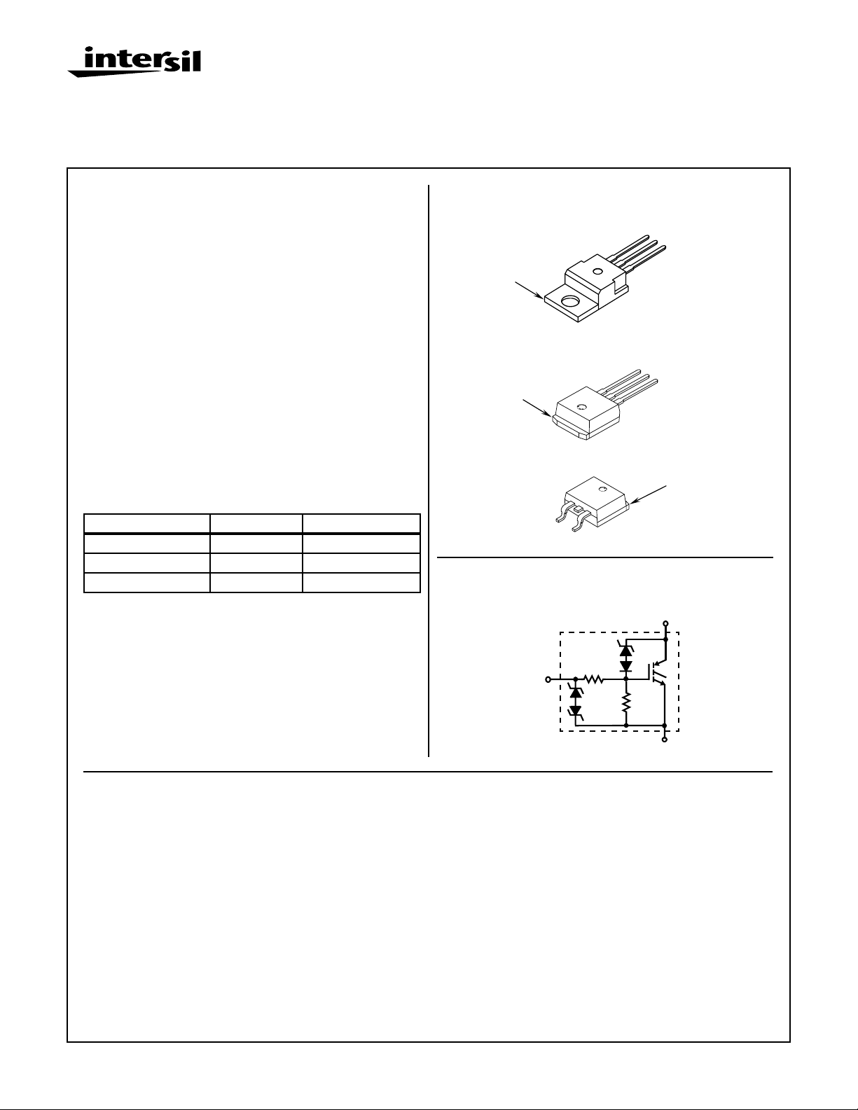
PACKAGING AVAILABILITY
PART NUMBER PACKAGE BRAND
HGTP14N36G3VL TO-220AB 14N36GVL
HGT1S14N36G3VL TO-262AA 14N36GVL
HGT1S14N36G3VLS TO-263AB 14N36GVL
NOTE: When ordering, use the entire part number. Add the suf fix 9A
to obtain the TO-263AB variant in the tape and reel, i.e.,
HGT1S14N36G3VLS9A.
The development type number for this device is TA49021.
Packages
JEDEC TO-220AB
COLLECTOR
(FLANGE)
JEDEC TO-262AA
COLLECTOR
(FLANGE)
JEDEC TO-263AB
GATE
EMITTER
Terminal Diagram
N-CHANNEL ENHANCEMENT MODE
GATE
EMITTER
COLLECTOR
GATE
EMITTER
COLLECTOR
GATE
A
A
M
A
R
1
COLLECTOR
(FLANGE)
COLLECTOR
R
2
EMITTER
Absolute Maximum Ratings T
= +25oC, Unless Otherwise Specified
C
HGTP14N36G3VL,
HGT1S14N36G3VL,
HGT1S14N36G3VLS UNITS
Collector-Emitter Bkdn Voltage at 10mA . . . . . . . . . . . . . . . . . . . . . . . . . . . . . . . . BV
Emitter-Collector Bkdn Voltage at 10mA . . . . . . . . . . . . . . . . . . . . . . . . . . . . . . . . BV
Collector Current Continuous at V
Gate-Emitter Voltage (Note). . . . . . . . . . . . . . . . . . . . . . . . . . . . . . . . . . . . . . . . . . . V
Inductive Switching Current at L = 2.3mH, T
at L = 2.3mH, T
Collector to Emitter Avalanche Energy at L = 2.3mH, T
Power Dissipation Total at T
Power Dissipation Derating T
Operating and Storage Junction Temperature Range . . . . . . . . . . . . . . . . . . . . .T
= 5V, TC = +25oC. . . . . . . . . . . . . . . . . . . . . . . I
GE
= 5V, TC = +100oC. . . . . . . . . . . . . . . . . . . . . .I
at V
GE
= +25oC . . . . . . . . . . . . . . . . . . . . . . .I
C
= + 175oC . . . . . . . . . . . . . . . . . . . . . .I
C
= +25oC . . . . . . . . . . . . . . . . . . . . . . . . . . . . . . . . . . . . P
C
> +25oC. . . . . . . . . . . . . . . . . . . . . . . . . . . . . . . . . . . . . . 0.67 W/oC
C
= +25oC. . . . . . . . . . . . . . . E
C
Maximum Lead Temperature for Soldering . . . . . . . . . . . . . . . . . . . . . . . . . . . . . . . . . .T
Electrostatic Voltage at 100pF, 1500Ω. . . . . . . . . . . . . . . . . . . . . . . . . . . . . . . . . . . . ESD 6 KV
NOTE: May be exceeded if I
CAUTION: These devices are sensitive to electrostatic discharge; follow proper IC Handling Procedures.
1-888-INTERSIL or 321-724-7143
is limited to 10mA.
GEM
| Copyright © Intersil Corporation 1999
3-55
CER
ECS
C25
C100
GEM
SCIS
SCIS
AS
D
, T
J
STG
L
390 V
24 V
18 A
14 A
±10 V
17 A
12 A
332 mJ
100 W
-40 to +175
260
File Number
o
C
o
C
4008
Page 2
Specifications HGTP14N36G3VL, HGT1S14N36G3VL, HGT1S14N36G3VLS
Electrical Specifications T
= +25oC, Unless Otherwise Specified
C
PARAMETERS SYMBOL TEST CONDITIONS
Collector-Emitter Breakdown Voltage BV
Gate-Emitter Plateau Voltage V
Gate Charge Q
Collector-Emitter Clamp Breakdown
Voltage
Emitter-Collector Breakdown Voltage BV
Collector-Emitter Leakage Current I
Collector-Emitter Saturation Voltage V
CER
GEP
G(ON)IC
BV
CE(CL)IC
ECS
CER
CE(SAT)IC
LIMITS
UNITSMIN TYP MAX
IC = 10mA,
TC = +175oC 320 355 400 V
VGE = 0V
RGE = 1kΩ
TC = +25oC 330 360 390 V
TC = -40oC 320 350 385 V
IC = 7A,
TC = +25oC - 2.7 - V
VCE = 12V
= 7A,
TC = +25oC - 24 - nC
VCE = 12V
= 7A
TC = +175oC 350 380 410 V
RG = 1000Ω
IC = 10mA TC = +25oC2428-V
VCE = 250V
TC = +25oC-- 25µA
RGE = 1kΩ
TC = +175oC - - 250 µA
= 7A
TC = +25oC - 1.25 1.45 V
VGE = 4.5V
TC = +175oC - 1.15 1.6 V
Gate-Emitter Threshold Voltage V
GE(TH)IC
Gate Series Resistance R
Gate-Emitter Resistance R
Gate-Emitter Leakage Current I
Gate-Emitter Breakdown Voltage BV
Current Turn-Off Time-Inductive Load t
D(OFF)I
t
F(OFF)I
Inductive Use Test I
Thermal Resistance R
GES
GES
SCIS
θJC
IC = 14A
TC = +25oC - 1.6 2.2 V
VGE = 5V
TC = +175oC - 1.7 2.9 V
= 1mA
VCE = V
GE
1
2
TC = +25oC 1.3 1.8 2.2 V
TC = +25oC - 75 - Ω
TC = +25oC 102030kΩ
VGE = ±10V ±330 ±500 ±1000 µA
I
= ±2mA ±12 ±14 - V
GES
+
IC = 7A, RL = 28Ω
-7-µs
RG = 25Ω, L = 550µH,
VCL = 300V, VGE = 5V,
TC = +175oC
L = 2.3mH,
TC = +175oC12--A
VG = 5V,
TC = +25oC17--A
- - 1.5
o
C/W
3-56
Page 3

HGTP14N36G3VL, HGT1S14N36G3VL, HGT1S14N36G3VLS
Typical Performance Curves
PULSE DURATION = 250µs, DUTY CYCLE <0.5%, V
25
CE
= 10V
PULSE DURATION = 250µs, DUTY CYCLE <0.5%, T
40
10V
20
30
15
20
10
o
+25
+175oC
5
, COLLECTOR-EMITTER CURRENT (A)
CE
I
0
VGE, GATE-TO-EMITTER VOLTAGE (V)
C
-40oC
21345
10
, COLLECTOR-EMITTER CURRENT (A)
CE
I
0
0246810
V
CE
, COLLECTOR-TO-EMITTER VOLTAGE (V)
FIGURE 1. TRANSFER CHARACTERISTICS FIGURE 2. SATURATION CHARACTERISTICS
35
30
25
20
15
TC = +175oC
VGE = 5.0V
V
= 4.5V
GE
V
= 4.0V
GE
35
VGE = 4.5V
30
25
20
15
3.5V
-40oC
5.0V
4.5V
4.0V
3.0V
2.5V
= +25oC
C
o
+25
+175oC
C
10
5
, COLLECTOR EMITTER CURRENT (A)
CE
I
0
, SATURATION VOLTAGE (V)
V
CE(SAT)
4
53210
FIGURE 3. COLLECTOR-EMITTER CURRENT AS A FUNCTION
OF SATURATION VOLTAGE
1.35
1.25
1.15
, SATURATION VOLTAGE (V)
CE(SAT)
V
1.05
-25 +25 +75 +125 +175
TJ, JUNCTION TEMPERATURE (oC)
ICE = 7A
VGE = 4.0V
VGE = 4.5V
VGE = 5.0V
FIGURE 5. SATURATION VOLTAGE AS A FUNCTION OF
JUNCTION TEMPERATURE
10
5
, COLLECTOR EMITTER CURRENT (A)
CE
I
0
01234 5
V
, SATURATION VOLTAGE (V)
CE(SAT)
FIGURE 4. COLLECTOR-EMITTER CURRENT AS A FUNCTION
OF SATURATION VOLTAGE
2.25
ICE = 14A
VGE = 4.0V
2.00
1.75
, SATURATION VOLTAGE (V)
CE(SAT)
V
1.50
-25 +25 +75
T
, JUNCTION TEMPERATURE (oC)
J
VGE = 4.5V
VGE = 5.0V
+125
+175
FIGURE 6. SATURATION VOLTAGE AS A FUNCTION OF
JUNCTION TEMPERATURE
3-57
Page 4

HGTP14N36G3VL, HGT1S14N36G3VL, HGT1S14N36G3VLS
Typical Performance Curves (Continued)
20
18
16
14
12
10
8
6
4
2
, COLLECTOR-EMITTER CURRENT (A)
CE
I
0
+25 +50 +75 +125 +150
, CASE TEMPERATURE (oC)
T
C
+100 +175
VGE = 5V
FIGURE 7. COLLECTOR-EMITTER CURRENT AS A FUNCTION
OF CASE TEMPERATURE
1E4
1E3
1E2
V
= 20V
ECS
1.2
1.1
1.0
0.9
0.8
0.7
NORMALIZED THRESHOLD VOLTAGE
0.6
GE(TH),
V
-25
+25 +75 +125 +175
T
, JUNCTION TEMPERATURE (oC)
J
ICE = 1ma
FIGURE 8. NORMALIZED THRESHOLD VOLTAGE AS A
FUNCTION OF JUNCTION TEMPERATURE
7.0
VCE = 300V, VGE = 5V
6.5
6.0
5.5
5.0
= 25Ω, L = 550µH
R
GE
I
= 37Ω,
R
L
CE
= 7A
1E1
LEAKAGE CURRENT (µA)
1E0
1E-1
+20 +60 +100 +140
V
= 250V
CES
T
, JUNCTION TEMPERATURE (oC)
J
FIGURE 9. LEAKAGE CURRENT AS A FUNCTION OF
JUNCTION TEMPERATURE
25
o
+25
C
20
+175oC
15
10
, INDUCTIVE SWITCHING CURRENT (A)
C
I
5
0
2
4
L, INDUCTANCE (mH)
6
V
GE
8
FIGURE 11. SELF CLAMPED INDUCTIVE SWITCHING
CURRENT AS A FUNCTION OF INDUCTANCE
+180
= 5V
4.5
TURN OFF TIME (µs)
4.0
(OFF)I,
t
3.5
3.0
+25 +50 + 75 +100 +150 +175+125
TJ, JUNCTION TEMPERATURE (oC)
FIGURE 10. TURN-OFF TIME AS A FUNCTION OF
JUNCTION TEMPERATURE
650
600
550
500
450
400
, ENERGY (mJ)
350
AS
E
300
250
200
10
150
= 5V
V
GE
o
+25
C
+175oC
0
2
4
L, INDUCTANCE (mH)
6
8
10
FIGURE 12. SELF CLAMPED INDUCTIVE SWITCHING ENERGY
AS A FUNCTION OF INDUCTANCE
3-58
Page 5

HGTP14N36G3VL, HGT1S14N36G3VL, HGT1S14N36G3VLS
Typical Performance Curves (Continued)
2000
1800
FREQUENCY = 1MHz
1600
C
1400
IES
1200
1000
800
600
C, CAPACITANCE (pF)
400
C
200
C
0
RES
OES
0 5 10 15 20 25
V
, COLLECTOR-TO-EMITTER VOLTAGE (V)
CE
FIGURE 13. CAPACITANCE AS A FUNCTION OF COLLECTOR-
EMITTER VOLTAGE
0
10
0.5
0.2
t
0.1
-1
10
0.05
PD
1
t
2
0.02
DUTY FACTOR, D = t1 / t
0.01
, NORMALIZED THERMAL RESPONSE
SINGLE PULSE
θJC
-2
Z
10
-5
10
-4
10
PEAK TJ = (PDX Z
-3
10
10
-2
θJC
10
X R
-1
2
) + T
θJC
C
1
0
10
10
t1, RECTANGULAR PULSE DURATION (s)
FIGURE 15. NORMALIZED TRANSIENT THERMAL
IMPEDANCE, JUNCTION TO CASE
REF IG= 1mA, RL= 1.7Ω, TC= +25oC
12
10
8
VCE= 12V
6
6
5
4
3
VCE= 4V
4
2
VCE= 8V
2
, COLLECTOR-EMITTER VOLTAGE (V)
CE
0
V
0
5
Q
15
10
, GATE CHARGE (nC)
G
20
25
1
0
30
FIGURE 14. GATE CHARGE WAVEFORMS
355
350
345
340
25oC
335
, COLLECTOR-EMITTER
BKDN VOLTAGE (V)
CER
330
BV
325
0
2000 4000 6000 8000 10000
175oC
RGE, GATE-TO- EMITTER RESISTANCE (Ω)
FIGURE 16. BREAKDOWN VOLTAGE AS A FUNCTION OF
GATE-EMITTER RESISTANCE
, GATE-EMITTER VOLTAGE (V)
GE
V
Test Circuits
2.3mH
C
R
= 25Ω
GEN
5V
FIGURE 17. SELF CLAMPED INDUCTIVE SWITCHING
CURRENT TEST CIRCUIT
R
G
DUT
G
E
R
L
V
DD
L = 550µH
C
1/R
= 1/R
G
R
10V
GEN
GEN
+ 1/R
= 50Ω
GE
G
R
GE
DUT
= 50Ω
+
-
V
CC
300V
E
FIGURE 18. CLAMPED INDUCTIVE SWITCHING TIME
TEST CIRCUIT
3-59
Page 6

HGTP14N36G3VL, HGT1S14N36G3VL, HGT1S14N36G3VLS
Handling Precautions for IGBT’s
Insulated Gate Bipolar Transistors are susceptible to gateinsulation damage by the electrostatic discharge of energy
through the devices. When handling these devices, care
should be exercised to assure that the static charge built in
the handler’s body capacitance is not discharged through
the device. With proper handling and application procedures, however, IGBT’s are currently being extensively used
in production by numerous equipment manufacturers in military, industrial and consumer applications, with virtually no
damage problems due to electrostatic discharge. IGBT’s can
be handled safely if the following basic precautions are
taken:
1. Prior to assembly into a circuit, all leads should be kept
shorted together either by the use of metal shorting
springs or by the insertion into conductive material such
as †“ECCOSORBD LD26” or equivalent.
2. When devices are removed by hand from their carriers,
the hand being used should be grounded by any suitable
means - for example, with a metallic wristband.
3. Tips of soldering irons should be grounded.
4. Devices should never be inserted into or removed from
circuits with power on.
5. Gate Voltage Rating -The gate-voltage rating of V
may be exceeded if I
is limited to 10mA.
GEM
† Trademark Emerson and Cumming, Inc
.
INTERSIL CORPORATION IGBT PRODUCT IS COVERED BY ONE OR MORE OF THE FOLLOWING U.S. PATENTS:
4,364,073 4,417,385 4,430,792 4,443,931 4,466,176 4,516,143 4,532,534 4,567,641
4,587,713 4,598,461 4,605,948 4,618,872 4,620,211 4,631,564 4,639,754 4,639,762
4,641,162 4,644,637 4,682,195 4,684,413 4,694,313 4,717,679 4,743,952 4,783,690
4,794,432 4,801,986 4,803,533 4,809,045 4,809,047 4,810,665 4,823,176 4,837,606
4,860,080 4,883,767 4,888,627 4,890,143 4,901,127 4,904,609 4,933,740 4,963,951
4,969,027
GEM
All Intersil semiconductor products are manufactured, assembled and tested under ISO9000 quality systems certification.
Intersil products are sold by description only. Intersil Corporation reserves the right to make changes in circuit design and/or specifications at any time without
notice. Accordingly, the reader is cautioned to verify that data sheets are current before placing orders. Information furnished by Intersil is believed to be accurate
and reliable. However, no responsibility is assumed by Intersil or its subsidiaries for its use; nor for any infringements of patents or other rights of third parties which
may result from its use. No license is granted by implication or otherwise under any patent or patent rights of Intersil or its subsidiaries.
For information regarding Intersil Corporation and its products, see web site http://www.intersil.com
Sales Office Headquarters
NORTH AMERICA
Intersil Corporation
P. O. Box 883, Mail Stop 53-204
Melbourne, FL 32902
TEL: (321) 724-7000
FAX: (321) 724-7240
EUROPE
Intersil SA
Mercure Center
100, Rue de la Fusee
1130 Brussels, Belgium
TEL: (32) 2.724.2111
FAX: (32) 2.724.22.05
3-60
ASIA
Intersil (Taiwan) Ltd.
Taiwan Limited
7F-6, No. 101 Fu Hsing North Road
Taipei, Taiwan
Republic of China
TEL: (886) 2 2716 9310
FAX: (886) 2 2715 3029
 Loading...