

Page 1
TM
Data Sheet February 2002
Direct Sequence Spread Spectrum
Baseband Processor
The Intersil HFA3861B Direct
Sequence Spread Spectrum (DSSS)
baseband processor is part of the
PRISM® 2.4GHz WLAN Chip Set,
and contains all the functions necessary for a full or half
duplex packet baseband transceiver.
The HFA3861B has on-board A/D’s and D/A for analog I and
Q inputs and outputs, for which the HFA3783 IF QMODEM is
recommended. Differential phase shift keying modulation
schemes DBPSK and DQPSK, with data scrambling
capability, are available along with Complementary Code
Keying to provide a variety of data rates. Built-in flexibility
allows the HFA3861B to be configured through a general
purpose control bus, for a range of applications. Both
Receive and Transmit AGC functions with 7-bit AGC control
obtain maximum performance in the analog portions of the
transceiver. The HFA3861B is housed in a thin plastic quad
flat package (TQFP) suitable for PCMCIA board
applications.
Ordering Information
TEMP.
PART NUMBER
RANGE (oC) PACKAGE PKG. NO.
HFA3861BIN -40 to 85 64 Ld TQFP Q64.10x10
HFA3861BIN96 -40 to 85 Tape and Reel
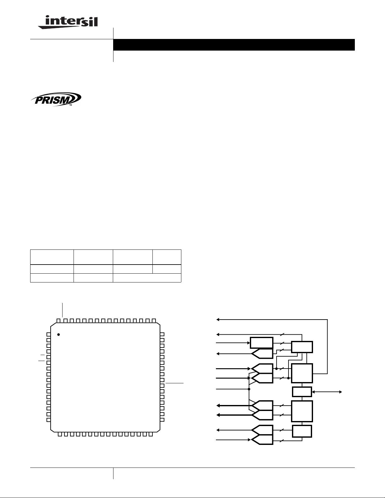
Pinout
HFA3861B
FN4816.2
Features
• Complete DSSS Baseband Processor
• Processing Gain. . . . . . . . . . . . . . . . . . . . FCC Compliant
• Programmable Data Rate. . . . . . . . 1, 2, 5.5, and 11Mbps
• Ultra Small Package. . . . . . . . . . . . . . . . . . . . . 10 x 10mm
• Single Supply Operation (44MHz Max) . . . . . 2.7V to 3.6V
• Modulation Methods. . . . . . . . DBPSK, DQPSK, and CCK
• Supports Full or Half Duplex Operations
• On-Chip A/D and D/A Converters for I/Q Data (6-Bit,
22MSPS), AGC, and Adaptive Power Control (7-Bit)
•Targeted for Multipath Delay Spreads ~50ns
• Supports Short Preamble Acquisition
• Supports Antenna Diversity
Applications
• Enterprise WLAN Systems
• Systems Targeting IEEE 802.11 Standard
• DSSS PCMCIA Wireless Transceiver
• Spread Spectrum WLAN RF Modems
• TDMA Packet Protocol Radios
•Part 15 Compliant Radio Links
•Portable PDA/Notebook Computer
• Wireless Digital Audio, Video, Multimedia
• PCN/Wireless PBX
• Wireless Bridges
GNDd
V
DDD
SD
SCLK
R/W
CS
GNDd
V
DDD
GNDa
RX_I+
RX_IV
DDA
RX_Q+
RX_Q-
GNDa
V
REF
ESET
SDI
R
TX_PE
RX_PE
CCA
6463 62 61 60 59 58 57 56 55 54 53 52 51 50 49
1
2
3
4
5
6
7
8
9
10
11
12
13
14
15
16
17 18 19 20 21 22 23 24 25 26 27 28 29 30 31 32
DDA
V
RX-IF_DET
TX_AGC_IN
I
GNDa
REF
TX_RDY
V
DDA
TXD
V
TX_I-
TX_I+
DDD
GNDd
GNDa
TXCLK
MD_RDY
RXD
GNDa
TX_Q+
COMPRES2
COMPCAP2
RXCLK
TEST7
TX_Q-
1
TEST6
TEST5
TEST4
48
TEST3
47
TEST2
46
TEST1
45
TEST0
44
GNDd
43
MCLK
42
NC
41
ANT-SEL
40
A
NT-SEL
39
RX-RF_AGC
38
V
37
DDD
GNDd
36
TX_IF_AGC
35
RX_IF_AGC
34
COMPCAP1
33
DDA
V
COMPRES1
CAUTION: These devices are sensitive to electrostatic discharge; follow proper IC Handling Procedures.
PRISM® is a registered trademark of Intersil Corporation. PRISM and design is a trademark of Intersil Corporation.
Simplified Block Diagram
ANT_SEL
RX_RF_AGC
RX_IF_DET
RX_IF_AGC
RX_I±
RX_Q±
V
REF
TX_I±
TX_Q±
TX_IF_AGC
TX_AGC_IN
44MHz MCLK
1-888-INTERSIL or 321-724-7143
THRESH.
DETECT
|
Intersil (and design) is a trademark of Intersil Americas Inc.
Copyright © Intersil Americas Inc. 2002. All Rights Reserved
IF
DAC
I ADC
Q ADC
I DAC
Q DAC
TX
DAC
TX
ADC
1
1
AGC
7
CTL
6
DEMOD
6
I/O
6
6
MOD
7
6
TX
ALC
HFA 3861B BBP
DATA I/O
Page 2
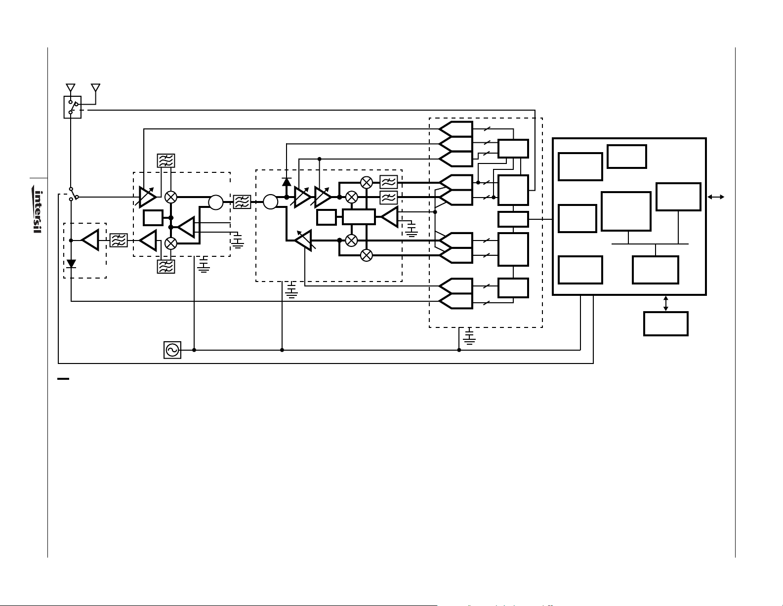
Typical Application Diagram
AntSel
2
PLL
HFA3963
RFPA
(FILE# 4635)
HFA3683A RF/IF
CONV (FILE# 4634)
Σ
REF IN
RF
LO
Σ
REF IN
I/O LO
PLL
HFA3783 QUAD IF
(FILE# 4633)
REFOUT
IF
LO
RF
DAC
RF
ADC
IF
DAC
I ADC
Q ADC
I DAC
Q DAC
TX
DAC
TX
ADC
REF IN
1
1
AGC
7
CTL
6
DEMOD
6
I/O
6
6
MOD
7
TX
ALC
6
HFA3861B BBP
(FILE# 4816)
RADIO
DATA
INTERFACE
RADIO
CONTROL
PORTS
GP SERIAL
PORTS
WEP
ENGINE
CPU
16-BIT
PIPELINED
CONTROL
PROCESSOR
HFA3841
(FILE# 4661)
INTERFACE
MEMORY
ACCESS
ARBITER
EXTERNAL
MEMORY
MAC
HOST
LOGIC
HOSTPC
INTERFACE
HFA3861B
T/Rsw
DIFFERENTIAL SIGNALS
44MHz MCLK
TYPICAL TRANSCEIVER APPLICATION CIRCUIT USING THE HFA3861B
For additional information on the PRISM® chip set, visit our web site
www.intersil.com or call 1-888-INTERSIL or 321-724-7143.
Page 3
HFA3861B
Pin Descriptions
NAME PIN TYPE I/O DESCRIPTION
V
(Analog) 12, 17, 22, 31Power DC power supply 2.7V - 3.6V (Not Hard wired Together On Chip).
DDA
V
(Digital) 2, 8, 37, 57 Power DC power supply 2.7 - 3.6V.
DDD
GNDa
(Analog)
GNDd (Digital) 1, 7, 36, 43, 56Ground DC power supply 2.7 - 3.6V, ground.
9, 15, 20,
25, 28,
Ground DC power supply 2.7 - 3.6V, ground (Not Hard wired Together On Chip).
V
REF
I
REF
RXI
, +/-
RXQ
, +/-
ANTSEL
ANTSEL 40 O The antenna select signal changes state as the receiver switches from antenna to antenna during the
RX_IF_DET 19 I Analog input to the receive power A/D converter for AGC control.
RX_IF_AGC 34 O Analog drive to the IF AGC control.
RX_RF_AGC 38 O Drive to the RF AGC stage attenuator. CMOS digital.
TX_AGC_IN 18 I Input to the transmit power A/D converter for transmit AGC control.
TX_IF_AGC 35 O Analog drive to the transmit IF power control.
TX_PE 62 I When active, the transmitter is configured to be operational, otherwise the transmitter is in standby
TXD 58 I TXD is an input, used to transfer MAC Payload Data Unit (MPDU) data from the MAC or network
TXCLK 55 O TXCLK is a clock output used to receive the data on the TXD from the MAC or network processor to
TX_RDY 59 O TX_RDY is an output to the external network processor indicating that Preamble and Header
CCA 60 O Clear Channel Assessment (CCA) is an output used to signal that the channel is clear to transmit. The
RXD 53 O RXD is an output to the external network processor transferring demodulated Header information and
RXCLK 52 O RXCLK is the bit clock output. This clock is used to transfer Header information and payload data
16 I Voltage reference for A/D’s and D/A’s.
21 I Current reference for internal ADC and DAC devices. Requires a 12k
10/11 I Analog input to the internal 6-bit A/D of the In-phase received data. Balanced differential 10+/11-.
13/14 I Analog input to the internal 6-bit A/D of the Quadrature received data. Balanced differential 13+/14-.
39 O The antenna select signal changes state as the receiver switches from antenna to antenna during the
acquisition process in the antenna diversity mode. This is a complement for ANTSEL (pin 40) for
differential drive of antenna switches.
acquisition process in the antenna diversity mode. This is a complement for ANTSEL (pin 39) for
differential drive of antenna switches.
mode. TX_PE is an input from the external Media Access Controller (MAC) or network processor to
the HFA3861B. The rising edge of TX_PE will start the internal transmit state machine and the falling
edge will initiate shut down of the state machine. TX_PE envelopes the transmit data except for the
last bit. The transmitter will continue to run for 4
down gracefully.
processor to the HFA3861B. The data is received serially with the LSB first. The data is clocked in the
HFA3861B at the rising edge of TXCLK.
the HFA3861B, synchronously. Transmit data on the TXD bus is clocked into the HFA3861B on the
rising edge. The clocking edge is also programmable to be on either phase of the clock. The rate of
the clock will be dependent upon the data rate that is programmed in the signalling field of the header.
information has been generated and that the HFA3861B is ready to receive the data packet from the
network processor over the TXD serial bus.
CCA may be configured to one of four possible algorithms. The CCA algorithm and its features are
described elsewhere in the data sheet.
Logic 0 = Channel is clear to transmit.
Logic 1 = Channel is NOT clear to transmit (busy).
This polarity is programmable and can be inverted.
data in a serial format. The data is sent serially with the LSB first. The data is frame aligned with
MD_RDY.
through the RXD serial bus to the network processor. This clock reflects the bit rate in use. RXCLK is
held to a logic “0” state during the CRC16 reception. RXCLK becomes active after the SFD has been
detected. Data should be sampled on the rising edge. This polarity is programmable and can be
inverted.
µ s after TX_PE goes inactive to allow the PA to shut
Ω resistor to ground.
3
Page 4
HFA3861B
Pin Descriptions
NAME PIN TYPE I/O DESCRIPTION
MD_RDY 54 O MD_RDY is an output signal to the network processor, indicating header data and a data packet are
RX_PE 61 I When active, the receiver is configured to be operational, otherwise the receiver is in standby mode.
SD 3 I/O SD is a serial bidirectional data bus which is used to transfer address and data to/from the internal
SCLK 4 I SCLK is the clock for the SD serial bus. The data on SD is clocked at the rising edge. SCLK is an input
SDI 64 I Serial Data Input in 3 wire mode described in Tech Brief 383. This pin is not used in the 4 wire interface
R/W 5IR/W is an input to the HFA3861B used to change the direction of the SD bus when reading or writing
CS 6ICS is a Chip select for the device to activate the serial control port. The CS doesn’t impact any of the
TEST 7:0 51, 50, 49,
48, 47, 46,
RESET 63 I Master reset for device. When active TX and RX functions are disabled. If RESET is kept low the
MCLK 42 I Master Clock for device. The nominal frequency of this clock is 44MHz. This is used internally to
TXI
+/-
TXQ
+/-
CompCap 33 I Compensation Capacitor.
CompCap2 26 I Compensation Capacitor.
CompRes1 32 I Compensation Resistor.
CompRes2 27 I Compensation Resistor.
NOTE: See CR10[3].
(Continued)
ready to be transferred to the processor. MD_RDY is an active high signal that signals the start of data
transfer over the RXD serial bus. MD_RDY goes active when the SFD (Note) is detected and returns
to its inactive state when RX_PE goes inactive or an error is detected in the header.
This is an active high input signal. In standby, RX_PE inactive, all RX A/D converters are disabled.
registers. The bit ordering of an 8-bit word is MSB first. The first 8 bits during transfers indicate the
register address immediately followed by 8 more bits representing the data that needs to be written or
read at that register. In the 4 wire interface mode, this pin is three-stated unless the R/W
clock and it is asynchronous to the internal master clock (MCLK). The maximum rate of this clock is
11MHz or one half the master clock frequency, whichever is lower.
described in this data sheet. It should not be left floating.
data on the SD bus. R/W must be set up prior to the rising edge of SCLK. A high level indicates read
while a low level is a write.
other interface ports and signals, i.e., the TX or RX ports and interface signals. This is an active low
signal. When inactive SD, SCLK, and R/W become “don’t care” signals.
I/O This is a data port that can be programmed to bring out internal signals or data for monitoring. These
bits are primarily reserved by the manufacturer for testing. A further description of the test port is given
45, 44
23/24 O TX Spread baseband I digital output data. Data is output at the chip rate. Balanced differential 23+/24-.
29/30 O TX Spread baseband Q digital output data. Data is output at the chip rate. Balanced differential
in the appropriate section of this data sheet.
HFA3861B goes into the power standby mode. RESET does not alter any of the configuration register
values nor does it preset any of the registers into default values. Device requires programming upon
power-up See the section on Control Register 12 bit 7 for important initialization information.
generate all other internal necessary clocks and is divided by 2 or 4 for the transceiver clocks.
29+/30-.
pin is high.
External Interfaces
There are three primary digital interface ports for the
HFA3861B that are used for configuration and during
normal operation of the device as shown in Figure 1. These
ports are:
• The
Control Port
read the status of the internal HFA3861B registers.
• The
TX Port
to be transmitted from the network processor.
• The
RX Port
demodulated data to the network processor.
In addition to these primary digital interfaces the device
includes a byte wide parallel
, which is used to configure, write and/or
, which is used to accept the data that needs
, which is used to output the received
Test Port
which can be
4
configured to output various internal signals and/or data. The
device can also be set into various power consumption
modes by external control. The HFA3861B contains three
Analog to Digital (A/D) converters and four Digital to Analog
converters. The analog interfaces to the HFA3861B include,
the In phase (I) and quadrature (Q) data component inputs/
outputs, and the RF and IF receive automatic gain control
and transmit output power control.
Page 5
HFA3861B
HFA3861B
ANALOG
INPUTS
REFERENCE
A/D
POWER
DOWN
SIGNALS
TEST
PORT
ANT_SEL
8
RXI
RXQ
AGC
V
REF
I
REF
TX_PE
RX_PE
RESET
TEST
AGC
TXI
TXQ
TXD
TXCLK
TX_RDY
RXD
RXC
MD_RDY
CS
SD
SCLK
R/W
SDI
ANALOG
OUTPUTS
TX_PORT
RX_PORT
CONTROL_PORT
FIGURE 1. EXTERNAL INTERFACES
Control Port (4 Wire)
The serial control port is used to serially write and read
data to/from the device. This serial port can operate up to a
11MHz rate or 1/2 the maximum master clock rate of the
device, MCLK (whichever is lower). MCLK must be running
and RESET must be inactive during programming. This
port is used to program and to read all internal registers.
The first 8 bits always represent the address followed
immediately by the 8 data bits for that register. The LSB of
the address is a don’t care, but reserved for future
expansion. The serial transfers are accomplished through
the serial data pin (SD). SD is a bidirectional serial data
bus. Chip Select (CS
), and Read/Write (R/W) are also
required as handshake signals for this port. The clock used
in conjunction with the address and data on SD is SCLK.
This clock is provided by the external source and it is an
input to the HFA3861B. The timing relationships of these
signals are illustrated in Figures 2 and 3. R/W
data is to be read, and low when it is to be written. CS
asynchronous reset to the state machine. CS
active (low) during the entire data transfer cycle. CS
is high when
is an
must be
selects
the serial control port device only. The serial control port
operates asynchronously from the TX and RX ports and it
can accomplish data transfers independent of the activity at
the other digital or analog ports.
The HFA3861B has 96 internal registers that can be
configured through the control port. These registers are
listed in the Configuration and Control Internal Register
table. Table 9 lists the configuration register number, a brief
name describing the register, the HEX address to access
each of the registers and typical values. The type indicates
whether the corresponding register is Read only (R) or
Read/Write (R/W). Some registers are two bytes wide as
indicated on the table (high and low bytes).
FIRST ADDRESS BIT FIRST DATABIT OUT
SCLK
SD
R/W
CS
7654321076543210
1234567 01234567
LSB DATA OUTMSBMSB ADDRESS IN
NOTES:
1. The HFA3861B always uses the rising edge of SCLK to sample address and data and to generate read data.
2. These figures show the controller using the falling edge of SCLK to generate address and data and to sample read data.
FIGURE 2. CONTROL PORT READ TIMING
SCLK
SD
R/W
7654321076543210
1234567 012345670
LSB DATA INMSBMSB ADDRESS IN
CS
FIGURE 3. CONTROL PORT WRITE TIMING
5
Page 6
HFA3861B
TX Port
The transmit data port accepts the data that needs to be
transmitted serially from an external data source. The data is
modulated and transmitted as soon as it is received from the
external data source. The serial data is input to the HFA3861B
through TXD using the next rising edge of TXCLK to clock it in
the HFA3861B. TXCLK is an output from the HFA3861B. A
timing scenario of the transmit signal handshakes and
sequence is shown on timing diagram Figure 4.
The external processor initiates the transmit sequence by
asserting TX_PE. TX_PE envelopes the transmit data packet
on TXD. The HFA3861B responds by generating a Preamble
and Header. Before the last bit of the Header is sent, the
HFA3861B begins generating TXCLK to input the serial data
on TXD. TXCLK will run until TX_PE goes back to its inactive
state indicating the end of the data packet. The user needs to
hold TX_PE high for as many clocks as there bits to transmit.
For the higher data rates, this will be in multiples of the
number of bits per symbol. The HFA3861B will continue to
output modulated signal for 4
to supply bits to flush the modulation path. TX_PE must be
held until the last data bit is output from the MAC/FIFO. The
minimum TX_PE inactive pulse required to restart the
preamble and header generation is 2.22
modulator is 4.22
µ
s.
µ
s after the last data bit is output,
µ s and to reset the
The HFA3861B internally generates the preamble and header
information from information supplied via the control registers.
The external source needs to provide only the data portion of
the packet and set the control registers. The timing diagram of
this process is illustrated on Figure 4. Assertion of TX_PE will
initialize the generation of the preamble and header. TX_RDY,
which is an output from the HFA3861B, is used (if needed) to
indicate to the external processor that the preamble has been
generated and the device is ready to receive the data packet
(MPDU) to be transmitted from the external processor.
Signals TX_RDY, TX_PE and TXCLK can be set individually,
by programming Configuration Register (CR) 1, as either
active high or active low signals.
The transmit port is completely independent from the
operation of the other interface ports including the RX port,
therefore supporting a full duplex mode.
RX Port
The timing diagram Figure 5 illustrates the relationships
between the various signals of the RX port. The receive data
port serially outputs the demodulated data from RXD. The
data is output as soon as it is demodulated by the HFA3861B.
RX_PE must be at its active state throughout the receive
operation. When RX_PE is inactive the device's receive
functions, including acquisition, will be in a stand by mode.
TXCLK
TX_PE
TXD
TX_RDY
NOTE: Preamble/Header and Data is transmitted LSB first. TXD shown generated from rising edge of TXCLK.
RXCLK
RX_PE
HEADER
FIELDS
PROCESSING
MD_RDY
RXD
PREAMBLE/HEADER
FIRST DATA BIT SAMPLED
LSB DATA PACKET
FIGURE 4. TX PORT TIMING
LSB DATA PACKET MSB
MSB
DATA
LAST DATA BIT SAMPLED
DEASSERTED WHEN LAST
CHIP OF MPDU CLEARS
MOD PATH OF 3861 EXCEPT FOR
TX FILTER AND D/A
NOTE: MD_RDY active after CRC16. See detailed timing diagrams (Figures 18, 19, 20).
FIGURE 5. RX PORT TIMING
6
Page 7
7
HFA3861B
RXCLK is an output from the HFA3861B and is the clock for
the serial demodulated data on RXD. MD_RDY is an output
from the HFA3861B and it may be set to go active after the
SFD or CRC fields. Note that RXCLK becomes active after
the Start Frame Delimiter (SFD) to clock out the Signal,
Service, and Length fields, then goes inactive during the
header CRC field. RXCLK becomes active again for the
data. MD_RDY returns to its inactive state after RX_PE is
deactivated by the external controller, or if a header error is
detected. A header error is either a failure of the CRC
check, or the failure of the received signal field to match
one of the 4 programmed signal fields. For either type of
header error, the HFA3861B will reset itself after reception
of the CRC field. If MD_RDY had been set to go active after
CRC, it will remain low.
MD_RDY and RXCLK can be configured through CR 1, bits
1 and 0 to be active low, or active high. The receive port is
completely independent from the operation of the other
interface ports including the TX port, supporting therefore a
full duplex mode.
RX I/Q A/D Interface
The PRISM baseband processor chip (HFA3861B) includes
two 6-bit Analog to Digital converters (A/Ds) that sample the
balanced differential analog input from the IF down
converter. The I/Q A/D clock, samples at twice the chip rate.
The nominal sampling rate is 22MHz.
The interface specifications for the I and Q A/Ds are listed in
Ta ble 1. The HFA3861B is designed to be DC coupled to the
HFA3783.
TABLE 1. I, Q, A/D SPECIFICATIONS
PARAMETER MIN TYP MAX
Full Scale Input Voltage (V
Input Bandwidth (-0.5dB) - 11MHz -
Input Capacitance (pF) - 2 -
Input Impedance (DC) 5k
(Sampling Frequency) - 22MHz -
f
S
The voltages applied to pin 16, V
the references for the internal I and Q A/D converters. In
addition, For a nominal I/Q input of 250mV
suggested V
voltage is 1.2V.
REF
) 0.90 1.00 1.10
P-P
Ω
and pin 21, I
REF
HFA3683 HFA3783
--
, the
P-P
REF
set
RX_RF_AGC
RX_IF_DET
RX_IF_AGC
RX_I±
RX_Q±
AGC Circuit
The AGC circuit is designed to optimize A/D performance for
the I and Q inputs by maintaining the proper headroom on
the 6-bit converters. There are two gain stages being
controlled. At RF, the gain control is a 30dB step in gain from
turning off the LNA. This RF gain control optimizes the
receiver dynamic range when the signal level is high and
maintains the noise figure of the receiver when it is needed
most. At IF the gain control is linear and covers the bulk of
the gain control range of the receiver.
The AGC sensing mechanism uses a combination of the
I and Q A/D converters and the detected signal level in the IF
to determine the gain settings. The A/D outputs are
monitored in the HFA3861B for the desired nominal level.
When it is reached, by adjusting the receiver gain, the gain
control is locked for the remainder of the packet.
RX_AGC_IN Interface
The signal level in the IF stage is monitored to determine
when to impose the up to 30dB gain reduction in the RF
stage. This maximizes the dynamic range of the receiver by
keeping the RF stages out of saturation at high signal levels.
When the IF circuits’ sensor output reaches 0.5V, the
HFA3861B comparator switches in the 30dB pad and
compensates the IF AGC and RSSI measures.
TX I/Q DAC Interface
The transmit section outputs balanced differential analog
signals from the transmit DACs to the HFA3783. These are
DC coupled and digitally filtered.
Test Port
The HFA3861B provides the capability to access a number of
internal signals and/or data through the Test port, pins TEST
7:0. The test port is programmable through configuration
register (CR 34). Any signal on the test port can also be read
from configuration register (CR50) via the serial control port.
Additionally, the transmit DACs can be configured to show
signals in the receiver via CR 14. This allows visibility to
analog like signals that would normally be very difficult to
capture.
1
THRESH.
DETECT
DAC
I ADC
Q ADC
1
AGC
7
6
6
CTL
DEMOD
IF
HFA3861B
FIGURE 6. AGC CIRCUIT
I/O
DATA I/O
Page 8
HFA3861B
TX
RX
Power Down Modes
The power consumption modes of the HFA3861B are
controlled by the following control signals.
Receiver Power Enable (RX_PE, pin 61), which disables the
receiver when inactive.
Tr ansmitter Power Enable (TX_PE, pin 62), which disables
the transmitter when inactive.
Reset (RESET
mode. The power down mode where, both RESET
RX_PE are used is the lowest possible power consumption
mode for the receiver. Exiting this mode requires a
maximum of 10
The contents of the Configuration Registers are not effected
by any of the power down modes. No reconfiguration is
required when returning to operational modes. Activation of
RESET does corrupt learned values of AGC settings and
noise floor values. Optimum receiver operation may not be
achieved until these values are reestablished (typically
<50
µ
s of operation in noise only needed). The power
savings of activating RESET must be weighed against this.
Ta ble 2 describes the power down modes available for the
HFA3861B (V
other inputs to the part (MCLK, SCLK, etc.) continue to run
except as noted.
, pin 63), which puts the receiver in a sleep
and
µ
s before the device is operational.
= 3.3V). The table values assume that all
CC
Transmitter Description
The HFA3861B transmitter is designed as a Direct
Sequence Spread Spectrum Phase Shift Keying (DSSS
PSK) modulator. It can handle data rates of up to 11Mbps
(refer to AC and DC specifications). The various modes of
the modulator are Differential Binary Phase Shift Keying
(DBPSK) for 1Mbps, Differential Quaternary Phase Shift
Keying (DQPSK) for 2Mbps, and Complementary Code
Keying (CCK) for 5.5Mbps and 11Mbps. These implement
data rates as shown in Table 3. The major functional blocks
of the transmitter include a network processor interface,
DPSK modulator, high rate modulator, a data scrambler and
a spreader, as shown in Figure 7. CCK is essentially a
quadra-phase form of M-ARY Orthogonal Keying. A
description of that modulation can be found in Chapter 5 of:
“Telecommunications System Engineering”, by Lindsey and
Simon, Prentis Hall publishing.
The preamble is always transmitted as the DBPSK
waveform while the header can be configured to be either
DBPSK, or DQPSK, and data packets can be configured for
DBPSK, DQPSK, or CCK. The preamble is used by the
receiver to achieve initial PN synchronization while the
header includes the necessary data fields of the
communications protocol to establish the physical layer
link. The transmitter generates the synchronization
preamble and header and knows when to make the DBPSK
to DQPSK or CCK switchover, as required.
TABLE 2. POWER DOWN MODES
AT
MODE RX_PE TX_PE RESET
SLEEP
STANDBY Inactive Inactive Inactive 1.5mA Both transmit and receive operations disabled. Device will resume its operational
NO CLOCK
DATA
MODULATION
DBPSK 22 00 00 1 1
DQPSK 22 01 01 2 1
CCK 22 10 10 5.5 1.375
CCK 22 11 11 11 1.375
Inactive Inactive Active 1mA Both transmit and receive functions disabled. Device in sleep mode. Control
Inactive Active Inactive 15mA Receiver operations disabled. Receiver will return in its operational state within 1 µ s
Active Inactive Inactive 50mA Transmitter operations disabled. Transmitter will return to its operational state within
Standby Active 300
I
CC
TABLE 3. BIT RATE TABLE EXAMPLES FOR MCLK = 44MHz
A/D SAMPLE CLOCK
(MHz)
44MHz DEVICE STATE
Interface is still active. Register values are maintained. Device will return to its active
state within 10
state within 1 µ s of RX_PE or TX_PE going active.
of RX_PE going active.
2 MCLKs of TX_PE going active.
µ A All inputs at V
TX SETUP CR 5
BITS 1, 0
µ s.
or GND.
CC
RX SIGNAL CR 63
BITS 7, 6 DATA RATE (Mbps)
SYMBOL RATE
(MSPS)
8
Page 9
HFA3861B
9
DATA
I
OUT
Q
OUT
CHIP
RATE
SYMBOL
RATE
I vs Q
802.11 DSSS BPSK 802.11 DSSS QPSK
1Mbps
BARKER
1 BIT ENCODED TO
ONE OF 2 CODE
WORDS
(TRUE-INVERSE)
11 CHIPS
11 MC/S 11 MC/S
1 MS/S 1 MS/S
2 BITS ENCODED
TO ONE OF
4 CODE WORDS
2Mbps
BARKER
11 CHIPS
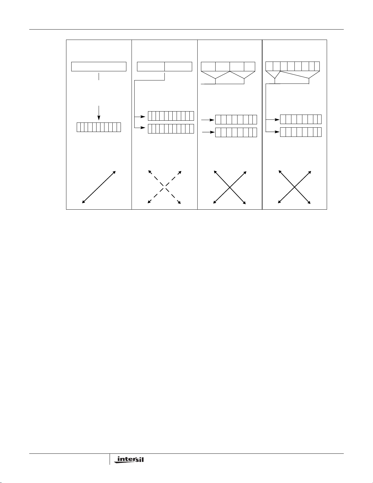
FIGURE 7. MODULATION MODES
5.5Mbps CCK
COMPLEX
SPREAD FUNCTIONS
4 BITS ENCODED
TO ONE OF 16
COMPLEX CCK
CODE WORDS
8 CHIPS
11 MC/S
1.375 MS/S
11Mbps CCK
COMPLEX
SPREAD FUNCTIONS
8 BITS ENCODED
TO ONE OF 256
COMPLEX CCK
CODE WORDS
8 CHIPS
11 MC/S
1.375 MS/S
For the 1 and 2Mbps modes, the transmitter accepts data
from the external source, scrambles it, differentially encodes
it as either DBPSK or DQPSK, and spreads it with the BPSK
PN sequence. The baseband digital signals are then output
to the external IF modulator.
For the CCK modes, the transmitter inputs the data and
partitions it into nibbles (4 bits) or bytes (8 bits). At 5.5Mbps,
it uses two of those bits to select one of 4 complex spread
sequences from a table of CCK sequences and then QPSK
modulates that symbol with the remaining 2 bits. Thus, there
are 4 possible spread sequences to send at four possible
carrier phases, but only one is sent. This sequence is then
modulated on the I and Q outputs. The initial phase
reference for the data portion of the packet is the phase of
the last bit of the header. At 11Mbps, one byte is used as
above where 6 bits are used to select one of 64 spread
sequences for a symbol and the other 2 are used to QPSK
modulate that symbol. Thus, the total possible number of
combinations of sequence and carrier phases is 256. Of
these only one is sent.
The bit rate Table 3 shows examples of the bit rates and the
symbol rates and Figure 7 shows the modulation schemes.
The modulator is completely independent from the
demodulator, allowing the PRISM baseband processor to be
used in full duplex operation.
Header/Packet Description
The HFA3861B is designed to handle packetized Direct
Sequence Spread Spectrum (DSSS) data transmissions.
The HFA3861B generates its own preamble and header
information. It uses two packet preamble and header
configurations. The first is backwards compatible with the
existing IEEE 802.11-1997 1 and 2Mbps modes and the
second is the optional shortened mode which maximizes
throughput at the expense of compatibility with legacy
equipment.
In the long preamble mode, the device uses a
synchronization preamble of 128 symbols along with a
header that includes four fields. The preamble is all 1's
(before entering the scrambler) plus a start frame delimiter
(SFD). The actual transmitted pattern of the preamble is
randomized by the scrambler. The preamble is always
transmitted as a DBPSK waveform (1Mbps). The duration of
the long preamble and header is 192
In the short preamble mode, the modem uses a
synchronization field of 56 zero symbols along with an SFD
transmitted at 1Mbps. The short header is transmitted at
2Mbps. The synchronization preamble is all 0’s to distinguish
it from the long header mode and the short preamble SFD is
the time reverse of the long preamble SFD. The duration of
the short preamble and header is 96
µ s.
µ s.
Page 10

HFA3861B
10
Start Frame Delimiter (SFD) Field (16 Bits) - This field is
used to establish the link frame timing. The HFA3861B will
not declare a valid data packet, even if it PN acquires, unless
it detects the SFD. The HFA3861B receiver is programmed
to time out searching for the SFD via CR 10 BITS 4 and 5.
The timer starts counting the moment that initial PN
synchronization has been established on the preamble.
The four fields for the header shown in Figure 8 are:
Signal Field (8 Bits) -
This field indicates what data rate the
data packet that follows the header will be. The HFA3861B
receiver looks at the signal field to determine whether it
needs to switch from DBPSK demodulation into DQPSK, or
CCK demodulation at the end of the preamble and header
fields.
Service Field (8 Bits) -
The MSB of this field is used to
indicate the correct length when the length field value is
ambiguous at 11Mbps. See IEEE STD 802.11 for definition
of the other bits. Bit 2 is used by the HFA3861B. To indicate
that the carrier reference and the bit timing references are
derived from the same oscillator.
Length Field (16 Bits) -
This field indicates the number of
microseconds it will take to transmit the payload data
(PSDU). The external controller (MAC) will check the length
field in determining when it needs to de-assert RX_PE.
CCITT - CRC 16 Field (16 Bits) -
This field includes the
16-bit CCITT - CRC 16 calculation of the three header fields.
This value is compared with the CCITT - CRC 16 code
calculated at the receiver. The HFA3861B receiver will
indicate a CCITT - CRC 16 error via CR24 bit 2 and will
lower MD_RDY and reset the receiver to the acquisition
mode if there is an error.
The CRC or cyclic Redundancy Check is a CCITT CRC-16
FCS (frame check sequence). It is the ones compliment of
the remainder generated by the modulo 2 division of the
protected bits by the polynomial:
16
12
x
+ x
+ x
5
+ 1
The protected bits are processed in transmit order. All CRC
calculations are made ahead of data scrambling. A shift
register with two taps is used for the calculation. It is preset
to all ones and then the protected fields are shifted through
the register. The output is then complemented and the
residual shifted out MSB first.
The following Configuration Registers (CR) are used to
program the preamble/header functions, more programming
details about these registers can be found in the Control
Registers section of this document:
CR 4 -
Defines the preamble length minus the SFD in
symbols. The 802.11 protocol requires a setting of
128d = 80h for the mandatory long preamble and 56d = 38h
for the optional short preamble.
CR 10 Bits 4, 5 -
Define the length of time that the
demodulator searches for the SFD before returning to
acquisition.
CR 5 Bits 0, 1 -
These bits of the register set the Signal field
to indicate what modulation is to be used for the data portion
of the packet.
CR 6 -
The value to be used in the Service field.
CR 7 and 8 -
Defines the value of the transmit data length
field. This value includes all symbols following the last
header field symbol and is in microseconds required to
transmit the data at the chosen data rate.
The packet consists of the preamble, header and MAC
protocol data unit (MPDU). The data is transmitted exactly
as received from the control processor. Some dummy bits
will be appended to the end of the packet to insure an
orderly shutdown of the transmitter. This prevents spectrum
splatter. At the end of a packet, the external controller is
expected to de-assert the TX_PE line to shut the
transmitter down. Set the scrambler CR36E37 seed valve
for the transmitter.
Scrambler and Data Encoder Description
The modulator has a data scrambler that implements the
scrambling algorithm specified in the IEEE 802.11 standard.
This scrambler is used for the preamble, header, and data in
all modes. The data scrambler is a self synchronizing circuit.
It consists of a 7-bit shift register with feedback from
specified taps of the register. Both transmitter and receiver
use the same scrambling algorithm. The scrambler can be
disabled by setting CR32 bit 2 to 1.
NOTE: Be advised that the IEEE 802.11 compliant scrambler in the
HFA3861B has the property that it can lock up (stop scrambling) on
random data followed by repetitive bit patterns. The probability of this
happening is 1/128. The patterns that have been identified are all
zeros, all ones, repeated 10s, repeated 1100s, and repeated
111000s. Any break in the repetitive pattern will restart the scrambler.
To insure that this does not cause any problem, the CCK waveform
uses a ping pong differential coding scheme that breaks up repetitive
0s patterns.
PREAMBLE (SYNC)
128/56 BITS
PREAMBLE
SFD
16 BITS
SIGNAL FIELD
8 BITS
FIGURE 8. 802.11 PREAMBLE/HEADER
SERVICE FIELD
8 BITS
HEADER
LENGTH FIELD
16 BITS
CRC16
16 BITS
Page 11

ce
j ϕ1ϕ2ϕ3ϕ
4
+++()
e
j ϕ1ϕ3ϕ
4
++()
e
j ϕ1ϕ2ϕ
4
++()
,
e
j ϕ1ϕ4+()ej ϕ1ϕ2ϕ
3
++()
e
j ϕ1ϕ3+() ej ϕ1ϕ2+()ejϕ
1
,–,,,–
,,
=
HFA3861B
11
Scrambling is done by a division using a prescribed
polynomial as shown in Figure 9. A shift register holds the
last quotient and the output is the exclusive-or of the data
and the sum of taps in the shift register. The taps are
programmable. The transmit scrambler seed for the long
preamble or for the short preamble can be set with CR36 or
CR37.
SERIAL
Z-5 Z-6 Z
DATA OUT
-7
SERIAL DATA
IN
XOR
Z-1 Z-2 Z-3 Z
FIGURE 9. SCRAMBLING PROCESS
-4
XOR
For the 1Mbps DBPSK data rates and for the header in all
rates, the data coder implements the desired DBPSK coding
by differential encoding the serial data from the scrambler
and driving both the I and Q output channels together. For
the 2Mbps DQPSK data rate, the data coder implements the
desired coding as shown in the DQPSK Data Encoder table.
This coding scheme results from differential coding of dibits
(2 bits). Vector rotation is counterclockwise although bits 6
and 7 of configuration register CR 1 can be used to reverse
the rotation sense of the TX or RX signal if desired.
TABLE 4. DQPSK DATA ENCODER
DIBIT PATTERN (d0, d1)
PHASE SHIFT
000
+90 01
+180 11
d0 IS FIRST IN TIME
For the 2Mbps DQPSK mode, the serial data is formed into
dibits or bit pairs in the differential encoder as detailed
above. One of the bits from the differential encoder goes to
the I Channel and the other to the Q Channel. The I and Q
Channels are then both multiplied with the 11-bit Barker
word at the spread rate. This forms QPSK modulation at the
symbol rate with BPSK modulation at the spread rate.
Transmit Filter Description
To minimize the requirements on the analog transmit
filtering, the transmit section shown in Figure 11 has an
output digital filter. This filter is a Finite Impulse Response
(FIR) style filter whose shape is set by tap coefficients. This
filter shapes the spectrum to meet the radio spectral mask
requirements while minimizing the peak to average
amplitude on the output. To meet the particular spread
spectrum processing gain regulatory requirements in Japan,
an extra FIR filter shape has been included that has a wider
main lobe. This increases the 90% power bandwidth from
about 11MHz to 14MHz. It has the unavoidable side effect of
increasing the amplitude modulation, so the available
transmit power is compromised by 2dB when using this filter
(CR 11 bit 5). The receive section Channel Matched Filter
(CMF) is also tailored to match the characteristics of the
transmit filter.
CCK Modulation
The spreading code length is 8 and based on
complementary codes. The chipping rate is 11Mchip/s and
the symbol duration is exactly 8 complex chips long. The
following formula is used to derive the CCK code words that
are used for spreading both 5.5 and 11Mbps:
Spread Spectrum Modulator Description
The modulator is designed to generate DBPSK, DQPSK, and
CCK spread spectrum signals. The modulator is capable of
automatically switching its rate where the preamble is
DBPSK modulated, and the data and/or header are
modulated differently. The modulator can support date rates
of 1, 2, 5.5 and 11Mbps. The programming details to set up
the modulator are given at the introductory paragraph of this
section. The HFA3861B utilizes Quadraphase (I/Q)
modulation at baseband for all modulation modes.
In the 1Mbps DBPSK mode, the I and Q Channels are
connected together and driven with the output of the
scrambler and differential encoder. The I and Q Channels
are then both multiplied with the 11-bit Barker word at the
spread rate. The I and Q signals go to the Quadrature
upconverter (HFA3724) to be modulated onto a carrier.
Thus, the spreading and data modulation are BPSK
modulated onto the carrier.
-90 10
(LSB to MSB), where c is the code word.
The terms:
ϕ
1, ϕ
2, ϕ
3, and ϕ
4 are defined below for
5.5Mbps and 11Mbps.
This formula creates 8 complex chips (LSB to MSB) that are
transmitted LSB first. The coding is a form of the generalized
Hadamard transform encoding where
chips,
ϕ 2 is added to all odd code chips, ϕ 3 is added to all
odd pairs of code chips and
ϕ
4 is added to all odd quads of
ϕ
1 is added to all code
code chips.
The phases
ϕ 1 modify the phase of all code chips of the
sequence and are DQPSK encoded for 5.5 and 11Mbps.
This will take the form of rotating the whole symbol by the
appropriate amount relative to the phase of the preceding
symbol. Note that the last chip of the symbol defined above
is the chip that indicates the symbol’s phase.
Page 12

HFA3861B
For the 5.5Mbps CCK mode, the output of the scrambler is
partitioned into nibbles. The first two bits are encoded as
differential modulation in accordance with Table 5 . All odd
numbered symbols of the short Header or MPDU are given
an extra 180 degree (π) rotation in addition to the standard
DQPSK modulation as shown in the table. The symbols of
the MPDU shall be numbered starting with “0” for the first
symbol for the purposes of determining odd and even
symbols. That is, the MPDU starts on an even numbered
symbol. The last data dibits d2, and d3 CCK encode the
basic symbol as specified in Table 6. This table is derived
from the formula above by setting ϕ2 = (d2*pi)+ pi/2, ϕ3 = 0,
and ϕ4 = d3*pi. In the table d2 and d3 are in the order shown
and the complex chips are shown LSB to MSB (left to right)
with LSB transmitted first.
TABLE 5. DQPSK ENCODING TABLE
EVEN SYMBOLS
DIBIT PATTERN (d(0), d(1))
d(0) IS FIRST IN TIME
00 0
01 π/2 3π/2 (-π/2)
11
10 3π/2 (-π/2) π/2
TABLE 6. 5.5Mbps CCK ENCODING TABLE
d2, d3
00 : 1j 1 1j -1 1j 1-1j 1
01 : -1j -1 -1j 11j 1-1j 1
10 : -1j 1 -1j -1 -1j 11j 1
11 : 1j -1 1j 1-1j 11j 1
PHASE CHANGE
(+jω)
π
ODD SYMBOLS
PHASE CHANGE
(+jω)
π
0
TABLE 7. QPSK ENCODING TABLE
DIBIT PATTERN (d(i), d(i+1))
d(i) IS FIRST IN TIME PHASE
00 0
01 π/2
10
11 3π/2 (-π/2)
π
TX Power Control
The transmitter power can be controlled by the MAC via two
registers. The first register, CR58, contains the results of
power measurements digitized by the HFA3861B. By
comparing this measurement to what the MAC needs for
transmit power, the MAC can determine whether to raise or
lower the transmit power. It does this by writing the power
level desired to register CR31.
Clear Channel Assessment (CCA) and
Energy Detect (ED) Description
The clear channel assessment (CCA) circuit implements the
carrier sense portion of a carrier sense multiple access (CSMA)
networking scheme. The Clear Channel Assessment (CCA)
monitors the environment to determine when it is feasible to
transmit. The CCA circuit in the HFA3861B can be programmed
to be a function of RSSI (energy detected on the channel),
CS1, SQ1, or both. The CCA output can be ignored, allowing
transmissions independent of any channel conditions. The CCA
in combination with the visibility of the various internal
parameters (i.e., Energy Detection measurement results), can
assist an external processor in executing algorithms that can
adapt to the environment. These algorithms can increase
network throughput by minimizing collisions and reducing
transmissions liable to errors.
At 11Mbps, 8 bits (d0 to d7; d0 first in time) are transmitted
per symbol.
The first dibit (d0, d1) encodes ϕ1 based on DQPSK. The
DQPSK encoder is specified in Table 6 above. The phase
change for ϕ1 is relative to the phase ϕ1 of the preceding
symbol. In the case of rate change, the phase change for ϕ1
is relative to the phase ϕ1 of the preceding CCK symbol. All
odd numbered symbols of the MPDU are given an extra 180
degree (π) rotation in accordance with the DQPSK
modulation as shown in Table 7. Symbol numbering starts
with “0” for the first symbol of the MPDU.
The data dibits: (d2, d3), (d4, d5), (d6, d7) encode ϕ2, ϕ3,
and ϕ4 respectively based on QPSK as specified in Table 7.
Note that this table is binary, not Grey, coded.
12
There are three measures that can be used in the CCA
assessment. The receive signal strength indication (RSSI)
which indicates the energy at the antenna, CS1 and carrier
sense (SQ1). SQ1 becomes active only when a spread
signal with the proper PN code has been detected, and the
peak correlation amplitude to sidelobe ratio exceeds a set
threshold, so it may not be adequate in itself.
CS1 becomes active anytime the AGC portion of the circuit
becomes unlocked, which is likely at the onset of a signal
that is strong enough to support 11Mbps, but may not occur
with the onset of a signal that is only strong enough to
support 1 or 2MBps. CS1 stays active until the AGC locks
and a SQ1 assessment is done, if SQ1 is false, then CS1 is
cleared, which deasserts CCA. If SQ1 is true, then tracking
is begun, and CCA continues to show the channel busy. CS1
may occur at any time during acquisition as the AGC state
machine runs asynchronously with respect to slot times.
Page 13

HFA3861B
A SQ1 evaluation occurs whenever the AGC has remained
locked for the entire data ingest period, when this happens,
SQ1 is updated between 8 and 9µs into the 10µs dwell. If
CS1 is not active, two consecutive SQ1’s are required to
advance the part to tracking.
The state of CCA is not guaranteed from the time RX_PE
goes high until the first CCA assessment is made. At the end
of a packet, after RXPE has been deasserted, the state of
CCA is also not guaranteed.
The receive signal strength indication (RSSI) measurement is
derived from the state of the AGC circuit. ED is the comparison
result of RSSI against a threshold. The threshold may be set to
an absolute power value, or it may be set to be N dB above the
measured noise floor. See CR 38. The HFA3861B measures
and stores the RSSI level when it detects no presence of BPSK
or QPSK signals. The smallest value of a 256 value buffer is
taken to be the noise floor. Thus, the value of the noise floor will
adapt to the environment. A separate noise floor value is
maintained for each antenna. An initial value of the noise floor
is established within 50µs of the chip being active and is refined
as goes on. Deasserting RX_PE does not corrupt the learned
values. If the absolute power metric is chosen, this threshold is
normally set to between -70 and -80dBm.
If desired, ED may be used in the acquisition process as well
as CCA. ED may be used to mask (squelch) weak signals
and prevent radio reception of signals too weak to support
the high data rates, signals from adjacent cells, networks, or
buildings. See CR48.
The Configuration registers effecting the CCA algorithm
operation are summarized below (more programming details
on these registers can be found under the Control Registers
section of this document).
channel to be busy and then become clear without an
MD_RDY occurring.
AGC Description
The AGC system consists of the 3 chips handling the receive
signal, the RF to IF downconverter, the IF to baseband
converter, and the baseband processor. The AGC loop is
digitally controlled by the BBP. Basically it operates as
follows:
Initially, the radio is set for high gain. The percent of time that
the A/D converters in the baseband processor are saturated
is monitored along with signal amplitude and the gain is
adjusted down until the amplitude is what will optimize the
demodulator’s performance. If the amount of saturation is
great, the initial gain adjust steps are large. If the signal
overload is small, they are less. When the gain is right and
the A/Ds’ outputs are within the lock window, the BBP
declares AGC lock and stops adjusting for the duration of the
packet. If the signal level then varies more than a preset
amount, the AGC is declared unlocked and the gain again
allowed to readjust.
The BBP looks for the locked state following an unlocked
state as one indication that a received signal is on the
antenna. This starts the receive process of looking for PN
correlation. Once PN correlation and AGC lock are found,
the processor begins acquisition.
For large signals, the power level in the RF stage output is
also monitored and if it is large, the LNA stage is shut down.
This removes 30dB of gain from the receive chain which is
compensated for by replacing 30dB of gain in the IF AGC
stage. There is some hysteresis in this operation. This
improves the receiver dynamic range.
The CCA output from pin 60 of the device can be defined as
active high or active low through CR 1 (bit 2).
CR9(6:5) allow CCA to be programmed to be a function of ED
only, the logical operation of (CS1 OR SQ1), the logical function
of (ED AND (CS1 OR SQ1)), or (ED OR (CS1 OR SQ1)).
CR11(3) lets the user select from sampled CCA mode,
which means CCA will not glitch, is updated once per
symbol and is valid for reading at 15.8µs or 19.8µs. In nonsampled mode, CCA may change at anytime, potentially
several times per slot, as ED and CS1 operate
asynchronously to slot times.
In a typical system CCA will be monitored to determine when
the channel is clear. Once the channel is detected busy,
CCA should be checked periodically to determine if the
channel becomes clear. CCA can be programmed to be
stable to allow asynchronous sampling or even falling edge
detection of CCA. Once MD_RDY goes active, CCA is then
ignored for the remainder of the message. Failure to monitor
CCA until MD_RDY goes active (or use of a time-out circuit)
could result in a stalled system as it is possible for the
13
Demodulator Description
The receiver portion of the baseband processor, performs A/D
conversion and demodulation of the spread spectrum signal.
It correlates the PN spread symbols, then demodulates the
DBPSK, DQPSK, or CCK symbols. The demodulator
includes a frequency tracking loop that tracks and removes
the carrier frequency offset. In addition it tracks the symbol
timing, and differentially decodes (where appropriate) and
descrambles the data. The data is output through the RX
Port to the external processor.
The PRISM baseband processor, HFA3861B uses differential
demodulation for the initial acquisition portion of the message
processing and then switches to coherent demodulation for
the MPDU demodulation. The HFA3861B is designed to
achieve rapid settling of the carrier tracking loop during
acquisition. Rapid phase fluctuations are handled with a
relatively wide loop bandwidth which is then stepped down as
the packet progresses. Coherent processing improves the
BER performance margin as opposed to differentially
coherent processing for the CCK data rates.
Page 14

HFA3861B
The baseband processor uses time invariant correlation to strip
the PN spreading and phase processing to demodulate the
resulting signals in the header and DBPSK/DQPSK
demodulation modes. These operations are illustrated in Figure
13 which is an overall block diagram of the receiver processor.
In processing the DBPSK header, input samples from the I and
Q A/D converters are correlated to remove the spreading
sequence. The peak position of the correlation pulse is used to
determine the symbol timing. The sample stream is decimated
to the symbol rate and corrected for frequency offset prior to
PSK demodulation. Phase errors from the demodulator are fed
to the NCO through a lead/lag filter to maintain phase lock. The
carrier is de-rotated by the carrier tracking loop. The
demodulated data is differentially decoded and descrambled
before being sent to the header detection section.
In the 1Mbps DBPSK mode, data demodulation is performed
the same as in header processing. In the 2Mbps DQPSK
mode, the demodulator demodulates two bits per symbol
and differentially decodes these bit pairs. The bits are then
serialized and descrambled prior to being sent to the output.
In the CCK modes, the receiver removes carrier frequency
offsets and uses a bank of correlators to detect the
modulation. A biggest picker finds the largest correlation in
the I and Q Channels and determines the sign of those
correlations. For this to happen, the demodulator must know
the starting phase which is determined by referencing the
data to the last bit of the header. Each symbol demodulated
determines 1 or 2 nibbles of data. This is then serialized and
descrambled before being passed to the output.
Chip tracking in the CCK modes is chip decision directed.
Carrier tracking is via a lead/lag filter using a digital Costas
phase detector.
Acquisition Description
A projected worst case time line for the acquisition of a
signal with a short preamble and header is shown. The
synchronization part of the preamble is 56 symbols long
followed by a 16-bit SFD. The receiver must monitor the
antenna to determine if a signal is present. The timeline is
broken into 10µs blocks (dwells) for the scanning process.
This length of time is necessary to allow enough integration
of the signal to make a good acquisition decision. This worst
case time line example assumes that the signal arrives part
way into the first dwell such as to just barely catch detection.
The signal and the scanning process are asynchronous and
the signal could start anywhere. In this timeline, it is
assumed that the signal is present in the first 10µs dwell, but
was missed due to power amplifier ramp up.
Meanwhile signal quality and signal frequency
measurements are made simultaneous with symbol timing
measurements. A CS1 followed by SQ1 active, or two
consecutive SQ1’s will cause the part to finish the acquisition
phase and enter the tracking phase.
Prior to initial acquisition the NCO was inactive and DPSK
demodulation processing was used. Carrier phase
measurement are done on a symbol by symbol basis
afterward and coherent DPSK demodulation is in effect.
After a brief setup time as illustrated on the timeline of, the
signal begins to emerge from the demodulator.
It takes 7 more symbols to seed the descrambler before
valid data is available. This occurs in time for the SFD to be
received. At this time the demodulator is tracking and in the
coherent PSK demodulation mode it will no longer
acquire signals.
Channel Matched Filter (CMF) Description
The receive section shown in Figure 13 operates on the RAKE
receiver principle which maximizes the SNR of the signal by
combining the energy of multipath signal components. The
RAKE receiver is implemented with a Channel Matched Filter
(CMF) using a FIR filter structure with 16 taps. The CMF is
programmed by calculating the Channel Impulse Response
(CIR) of the channel and mathematically manipulating that to
form the tap coefficients of the CMF. Thus, the CMF is set to
compensate the channel characteristics that distort the signal.
Since the calculation of the CIR is inaccurate at low SNR or in
the presence of strong CW interference, the chip has
thresholds (CR 35, 49) that are set to substitute a default CMF
shape under those conditions. This default CMF shape is
designed to compensate only the known transmit and receive
non linearity.
TX
POWER
RAMP
56 SYMBOL SYNC
2 20 SYMBOLS
AGC SETTLE AND LOCK VERIFY AND CIR/FREQUENCY
AND INITIAL DETECTION ESTIMATION AND CMF/NCO
FIGURE 10. ACQUISITION TIMELINE, NON DIVERSITY
20 SYMBOLS 7 SYM 16 SYMBOLS
JAMMING
14
SEED
DESCRAMBLER
START SFD DETECTION
SFD
SFD DET
START DATA
Page 15

HFA3861B
I
REF
V
REF
TX_AGC_IN (18)
TX_IF_AGC (35)
ANTSEL (39)
ANTSEL (40)
(21)
(16)
(ANALOG)
V
DD
(12, 17, 22, 31)
6-BIT
ADC
6-BIT
DAC
(9, 15, 20, 25, 28)
TX AGC
CONTROL
REGISTER
GND (ANALOG)
TRANSMIT
MODULATOR,
BARKER/CCK
FILTER
TEST CONTROL
(DIGITAL)
V
DD
(2, 8, 37, 57)
PREAMBLE/HEADER
CRC-16
GENERATOR
TX_DATA
SCRAMBLER
GND (DIGITAL)
(1, 7, 36, 43, 56)
OUTPUT MUX
OUTPUT MUX
DAC
DAC
PORT
TRANSMIT
(52) RXCLK
(60) CCA
TXI (23, 24)
TXQ (29, 30)
(59) TX_RDY
(55) TXCLK
(58) TXD
TIMING
GENERATOR
MCLK
(62) TX_PE
(42)
MCLK
FIGURE 11. DSSS BASEBAND PROCESSOR, TRANSMIT SECTION
PN Correlators Description
There are two types of correlators in the HFA3861B baseband
processor. The first is a parallel matched correlator that
correlates for the Barker sequence used in preamble, header,
and PSK data modes. This PN correlator is designed to handle
BPSK spreading with carrier offsets up to ±50ppm and 11 chips
per symbol. Since the spreading is BPSK, the correlator is
implemented with two real correlators, one for the I and one for
the Q Channel. The same Barker sequence is always used for
both I and Q correlators.
These correlators are time invariant matched filters otherwise
known as parallel correlators. They use one sample per chip for
TX
STATE
CONTROL
TEST PORT
(45)
(44) (46)
TEST 0
TEST 1
(47)
TEST 2
(48)
TEST 3
(49)
TEST 4
PROCESSOR INTERFACE
(50)
TEST 5
SERIAL CONTROL
(51)
TEST 6
PORT
TEST 7
(3) SD
(4) SCLK
(64) SDI
(5) R/W
(6) CS
correlation although two samples per chip are processed. The
correlator despreads the samples from the chip rate back to the
original data rate giving 10.4dB processing gain for 11 chips per
bit. While despreading the desired signal, the correlator
spreads the energy of any non correlating interfering signal.
The second form of correlator is the correlator function used for
detection of the CCK modulation. For the CCK modes, the
correlation function uses a Fast Walsh Transform to correlate
the 4 or 64 code possibilities followed by a biggest picker. The
biggest picker finds the biggest of 4 or 64 correlator outputs
depending on the rate. This is translated into 2 or 6 bits. The
15
Page 16

HFA3861B
detected output is then processed through the differential
decoder to demodulate the last two bits of the symbol.
Data Demodulation and Tracking
Description (DBPSK and DQPSK Modes)
The signal is demodulated from the correlation peaks
tracked by the symbol timing loop (bit sync) as shown in
Figure 12. The frequency and phase of the signal is
corrected using the NCO that is driven by the phase locked
loop. Demodulation of the DBPSK data in the early stages of
acquisition is done by differential detection. Once phase
locked loop tracking of the carrier is established, coherent
demodulation is enabled for better performance. Averaging
the phase errors over 10 symbols gives the necessary
frequency information for proper NCO operation.
Configuration Register 10 sets the search timer for the SFD.
This register sets this time-out length in symbols for the
receiver. If the time out is reached, and no SFD is found, the
receiver resets to the acquisition mode. The suggested value is
the number of preamble symbols plus 16. If different transmit
preamble lengths are used by various transmitters in a network,
the longest value should be used for the receiver settings.
Data Decoder and Descrambler
Description
The data decoder that implements the desired DQPSK
coding/decoding as shown in Table 8. The data is formed
into pairs of bits called dibits. The left bit of the pair is the first
in time. This coding scheme results from differential coding
of the dibits. Vector rotation is counterclockwise for a positive
phase shift, but can be reversed with bit 7 or 6 of CR 1.
For DBPSK, the decoding is simple differential decoding.
TABLE 8. DQPSK DATA DECODER
DIBIT PATTERN (D0, D1)
PHASE SHIFT
000
+90 01
+180 11
-90 10
D0 IS FIRST IN TIME
The data scrambler and de-scrambler are self synchronizing
circuits. They consist of a 7-bit shift register with feedback of
some of the taps of the register. The scrambler is designed to
insure smearing of the discrete spectrum lines produced by the
PN code. One thing to keep in mind is that both the differential
decoding and the descrambling cause error extension or burst
errors. This is due to two properties of the processing. First, the
differential decoding process causes errors to occur on pairs of
symbols. When a symbol’s phase is in error, the next symbol
will also be decoded wrong since the data is encoded in the
change in phase from one symbol to the next. Thus, two errors
are made on two successive symbols. Therefore up to 4 bits
may be wrong although on the average only 2 are. In QPSK
mode, these may occur next to one another or separated by up
to 2 bits. In the CCK mode, when a symbol decision error is
made, up to 6 bits may be in error although on average only 3
bits will be in error. Secondly, when the bits are processed by
the descrambler, these errors are further extended. The
descrambler is a 7-bit shift register with two taps exclusive or’ed
with the bit stream. Thus, each error is extended by a factor of
three. Multiple errors can be spaced the same as the tap
spacing, so they can be canceled in the descrambler. In this
case, two wrongs do make a right. Given all that, if a single
error is made the whole packet is discarded anyway, so the
error extension property has no effect on the packet error rate.
SAMPLES
AT 2X CHIP
RATE
CORRELATOR OUTPUT IS
THE RESULT OF CORRELATING
THE PN SEQUENCE WITH THE
T0
RECEIVED SIGNAL
16
CORRELATION TIME
FIGURE 12. CORRELATION PROCESS
T0 + 1 SYMBOL
CORRELATOR
OUTPUT
REPEATS
Descrambling is self synchronizing and is done by a
polynomial division using a prescribed polynomial. A shift
register holds the last quotient and the output is the exclusiveor of the data and the sum of taps in the shift register.
CORRELATION
PEAK
T0 + 2 SYMBOLS
EARLY
ON-TIME
LATE
Page 17

HFA3861B
RX_IF_DET (19)
RX_IF_AGC (34)
RX-RF-AGC (38)
RXI (10, 11)
RXQ (13, 14)
V
DD
(12, 17, 22, 31)
6-BIT
DAC
6-BIT
A/D
6-BIT
A/D
(ANALOG)
CONTROL
6
SAMPLE
6
AGC
CHANNEL
INTERPOLATOR,
GND (ANALOG)
(9, 15, 20, 25, 28)
MATCHED FILTER
CLEAR CHANNEL
ASSESSMENT/
SIGNAL QUALITY
DESPIN
(DIGITAL)
V
DD
(2, 8, 37, 57)
BARKER
CORRELATOR
TRAINING
8
EXTRACT.
8
SYMBOL
TRACKING
CMF
PEAK
GND (DIGITAL)
(1, 7, 36, 43, 56)
BIT
SYNC
DPSK
DEMOD
RX_DATA
DESCRAMBLER
PORT
RECEIVE
(60) CCA
(53) RXD
(52) RXCLK
ANTSEL (40)
ANTSEL (39)
ANTENNA
SWITCH
CONTROL
(63)
RESET
TIMING
GENERATOR
MCLK
(61)
RX_PE
(42)
MCLK
NCO
RECEIVE
STATE
MACHINE
CHIP
DE
COVER
CORREL
LOOP
FILTER
CCK
SYMBOL
DECISION
TEST CONTROL
(45)
(44) (46)
MUX
MUX
(47)
CRC-16 DETECT
PREAMBLE/HEADER
6-BIT
DAC
6-BIT
DAC
TEST PORT
(48)
(49)
(50)
(54) MD_RDY
(3) SD
(4) SCLK
(64) SDI
PORT
SERIAL CONTROL
(51)
(5) R/W
(6) CS
TXI (23, 24)
TXQ (29, 30)
TEST 0
TEST 1
FIGURE 13. DSSS BASEBAND PROCESSOR, RECEIVE SECTION
17
TEST 2
TEST 3
TEST 4
TEST 5
TEST 6
TEST 7
Page 18

HFA3861B
Data Demodulation in the CCK Modes
In this mode, the demodulator uses Complementary Code
Keying (CCK) modulation for the two highest data rates. It is
slaved to the low rate processor which it depends on for
acquisition of initial timing and phase tracking information.
The low rate section acquires the signal, locks up symbol
and carrier tracking loops, and determines the data rate to
be used for the MPDU data.
The demodulator for the CCK modes takes over when the
preamble and header have been acquired and processed.
On the last bit of the header, the phase of the signal is
captured and used as a phase reference for the high rate
differential demodulator.
The signal from the A/D converters is carrier frequency and
phase corrected by a DESPIN stage. This removes the
frequency offset and aligns the I and Q Channels properly for
the correlators. The sample rate is decimated to 11MSPS for
the correlators after the DESPIN since the data is now
synchronous in time.
The demodulator knows the symbol timing, so the
correlation is batch processed over each symbol. The
correlation outputs from the correlator are compared to each
other in a biggest picker and the chosen one determines 6
bits of the symbol. The QPSK phase of the chosen one
determines two more bits for a total of 8 bits per symbol. Six
bits come from which of the 64 correlators had the largest
output and the last two are determined from the QPSK
differential demod of that output. In the 5.5Mbps mode, only
4 of the correlator outputs are monitored. This demodulates
2 bits for which of 4 correlators had the largest output and 2
more for the QPSK demodulation of that output for a total of
4 bits per symbol.
Tracking
Carrier tracking is performed on the de-rotated signal
samples from the complex multiplier in a four phase Costas
loop. This forms the error term that is integrated in the lead/lag
filter for the NCO, closing the loop. Tracking is only measured
when there is a chip transition. Note that this tracking is
dependent on a positive SNR in the chip rate bandwidth.
The symbol clock is tracked by a sample interpolator that
can adjust the sample timing forwards and backwards by 72
increments of 1/8th chip. This approach means that the
HFA3861B can only track an offset in timing for a finite
interval before the limits of the interpolator are reached.
Thus, continuous demodulation is not possible.
Locked Oscillator Tracking
Bit timing tracking can be slaved to the carrier offset tracking
for improved performance as long as at both the transmitting
and the receiving radios, the bit clocks and carrier frequency
clocks are locked to common crystal oscillators. A bit carried
in the SERVICE field (bit 2) indicates whether or not the
transmitter has locked clocks. When the same bit is set at
the receiver (CR6 bit 2), the receiver knows it can track the
bit clock by counting down the carrier tracking offset. This is
much more accurate than tracking the bit clock directly. CR3
bit 6 can enable or disable this capability.
Demodulator Performance
This section indicates the typical performance measures for
a radio design. The performance data below should be used
as a guide. In general, the actual performance depends on
the application, interference environment, RF/IF
implementation and radio component selection.
Overall Eb/N0 Versus BER Performance
The PRISM chip set has been designed to be robust and
energy efficient in packet mode communications. The
demodulator uses coherent processing for data
demodulation. The figures below show the performance of
the baseband processor when used in conjunction with the
HFA3783 IF and the PRISM recommended IF filters. Off the
shelf test equipment are used for the RF processing. The
curves should be used as a guide to assess performance in
a complete implementation.
Factors for carrier phase noise, multipath, and other
degradations will need to be considered on an
implementation by implementation basis in order to predict
the overall performance of each individual system.
Figure 14 shows the curves for theoretical DBPSK/DQPSK
demodulation with coherent demodulation and
descrambling as well as the PRISM performance measured
for DBPSK and DQPSK. The theoretical performance for
DBPSK and DQPSK are the same as shown on the
diagram. Figure 15 shows the theoretical and actual
performance of the CCK modes. The losses in both figures
include RF and IF radio losses; they do not reflect the
HFA3861B losses alone. The HFA3861B baseband
processing losses from theoretical are, by themselves, a
small percentage of the overall loss.
The PRISM demodulator performs with an implementation
loss of less than 3dB from theoretical in a AWGN
environment with low phase noise local oscillators. For the
1 and 2Mbps modes, the observed errors occurred in
groups of 4 and 6 errors. This is because of the error
extension properties of differential decoding and
descrambling. For the 5.5 and 11Mbps modes, the errors
occur in symbols of 4 or 8 bits each and are further
extended by the descrambling. Therefore the error patterns
are less well defined.
18
Page 19

141312111098765
BER
Eb/N0
1.E+00
1.E-03
1.E-04
1.E-05
1.E-07
1.E-08
1.E-02
1.E-06
1.E-01
1.E-09
BER 11
BER 5.5
THY 5.5
THY 11
HFA3861B
7891011 12
THY 1, 2
FIGURE 14. BER vs Eb/N0 PERFORMANCE FOR PSK MODES FIGURE 15. BER vs Eb/N0 PERFORMANCE FOR CCK MODES
Clock Offset Tracking Performance
The PRISM baseband processor is designed to accept
data clock offsets of up to ±25ppm for each end of the link
(TX and RX). This effects both the acquisition and the
tracking performance of the demodulator. The budget for
clock offset error is 0.75dB at ±50ppm. No appreciable
degradation was seen for operation in AWGN at ±50ppm.
Eb/N0
BER 2.0
BER 1.0
1.E+00
1.E-01
1.E-02
1.E-03
1.E-04
1.E-05
1.E-06
1.E-07
1.E-08
BER
Carrier Offset Frequency Performance
The correlators used for acquisition for all modes and for
demodulation in the 1 and 2Mbps modes are time invariant
matched filter correlators otherwise known as parallel
correlators. They use two samples per chip and are tapped
at every other shift register stage. Their performance with
carrier frequency offsets is determined by the phase roll rate
due to the offset. For an offset of +50ppm (combined for both
TX and RX) will cause the carrier to phase roll 22.5 degrees
over the length of the correlator. This causes a loss of
0.22dB in correlation magnitude which translates directly to
Eb/N0 performance loss. In the PRISM chip design, the
carrier phase locked loop is inactive during acquisition.
During tracking, the carrier tracking loop corrects for offset,
so that no degradation is noted. In the presence of high
multipath and high SNR, however, some degradation is
expected.
19
Page 20

HFA3861B
A Default Register Configuration
The registers in the HFA3861B are addressed with 7-bit
numbers where the lower 1 bit of an 8-bit hexadecimal address
is left as unused. This results in the addresses being in
increments of 2 as shown in the table below. Table 9 shows the
register values for a default 802.11 configuration with various
rate configurations. The data is transmitted as either DBPSK,
TABLE 9. CONTROL REGISTER VALUES FOR DUAL ANTENNA DIVERSITY
CONFIGURATION
REGISTER NAME TYPE
CR0 Part/Version Code R 00 13
CR1 I/O Polarity R/W 02 00
CR2 I Cover Code R/W 04 48
CR3 Q Cover Code R/W 06 48
CR4 TX Preamble Length R/W 08 80
CR5 TX Signal Field R/W 0A 03
CR6 TX Service Field R/W 0C As Required
CR7 TX Length Field, High R/W 0E As Required
CR8 TX Length Field, Low R/W 10 As Required
CR9 RX/TX Configure R/W 12 A0
CR10 RX Configure R/W 14 B8
CR11 RX/TX Configure R/W 16 1B
CR12 A/D Test Modes 1 R/W 18 00
CR13 A/D Test Modes 2 R/W 1A 00
CR14 A/D Test Modes 3 R/W 1C 00
CR15 AGC GainClip R/W 1E 5C
CR16 AGC LowerSatCount R/W 20 82
CR17 AGC TimerCount R/W 22 20
CR18 AGC HiSat R/W 24 C4
CR19 AGC LockinLevel/CW detect threshold R/W 26 16
CR20 AGC LockWindow, pos side R/W 28 0A
CR21 AGC Threshold R/W 2A 16
CR22 AGC Lookup Table Addr and Control R/W 2C (Note 3)
CR23 AGC Lookup Table Data R/W 2E (Note 3)
CR24 AGC LoopGain R/W 30 2D
CR25 AGC RX_IF R/W 32 20
CR26 AGC Test Modes R/W 34 90
CR27 AGC RX_RF Threshold R/W 36 18
CR28 AGC Low SatAtten R/W 38 76
CR29 AGC LockWindow, negative side R/W 3A 0A
CR30 Carrier Sense 2 R/W 3C 24
CR31 Manual TX Power Control R/W 3E BA
CR32 Test Modes 1 R/W 40 00
CR33 Test Modes 2 R/W 42 00
CR34 Test Bus Address R/W 44 00
CR35 CMF Coefficient Control R/W 46 0C
CR36 Scrambler Seed, Long Preamble Option R/W 48 26
CR37 Scrambler Seed, Short Preamble Option R/W 4A 5B
CR38 ED Threshold R/W 4C 0C
CR39 CMF Gain Threshold R/W 4E 29
DQPSK, or CCK depending on the configuration chosen. It is
recommended that you start with the simplest configuration
(DBPSK) for initial test and verification of the device and/or the
radio design. The user can later modify the CR contents to
reflect the system and the required performance of each
specific application.
REGISTER
ADDRESS HEX 1/2/5.5/11Mbps
20
Page 21

HFA3861B
TABLE 9. CONTROL REGISTER VALUES FOR DUAL ANTENNA DIVERSITY (Continued)
CONFIGURATION
REGISTER NAME TYPE
CR40 Threshold for antenna decision R/W 50 0F
CR41 Preamble tracking loop lead coefficient R/W 52 20
CR42 Preamble tracking loop lag coefficient R/W 54 20
CR43 Header tracking loop lead coefficient R/W 56 10
CR44 Header tracking loop lag coefficient R/W 58 10
CR45 Data tracking loop lead coefficient R/W 5A 10
CR46 Data tracking loop lag coefficient R/W 5C 10
CR47 RF attenuator value R/W 5E 1E
CR48 ED and SQ1 control and SQ1 scale factor R/W 60 1E
CR49 Read only register mux control for registers 50 to 63 R/W 62 00
CR50 a&b: Test Bus Read R 64 N/A
CR51 a: Noise floorAntA
b: Signal Quality Measure Based on Carrier Tracking
CR52 a: Noise floorAntB
b: Received Signal Field
CR53 a: AGC error
b: Received Service Field
CR54 b: Received Length Field, Low R 6C N/A
CR55 b: Received Length Field, High R 6E N/A
CR56 b: Calculated CRC on Received Header, Low R 70 N/A
CR57 b: Calculated CRC on Received Header, High R 72 N/A
CR58 b: TX Power Measurement R 74 N/A
CR59 b: RX Mean Power R 76 N/A
CR60 b: RX_IF AGC R 78 N/A
CR61 b: RX Status Reg R 7A N/A
CR62 b: RSSI R 7C N/A
CR63 b: RX Status Reg R 7E N/A
NOTE:
3. This register is written, then the data is loaded into register 23 as per the following table.
REGISTER
ADDRESS HEX 1/2/5.5/11Mbps
R66N/A
R68N/A
R6AN/A
AGC REGISTER SETTINGS
CR22
DECIMAL
00 0C
01 10
02 14
03 18
04 1C
05 20
06 24
07 28
08 2E
09 34
10 38
11 3C
12 3F
13 43
14 46
15 48
21
CR23
HEX
AGC REGISTER SETTINGS (Continued)
CR22
DECIMAL
16 4B
17 50
18 55
19 5A
20 63
21 6D
22 76
23 7F
24 7F
25 7F
26 7F
27 7F
28 7F
29 7F
30 7F
31 7F
CR23
HEX
Page 22

HFA3861B
Control Registers
The following tables describe the function of each control register along with the associated bits in each control register.
CONFIGURATION REGISTER 0 ADDRESS (0h) R PART/VERSION CODE
Bit 7:4 Part Code
0001 = HFA3861B series
Bit 3:0 Version Code
0011 = 3861B Version
CONFIGURATION REGISTER 1 ADDRESS (02h) R/W I/O POLARITY
This register is used to define the phase of clocks and other interface signals. 00h is normal setting.
Bit 7 This control bit selects the phase of the receive carrier rotation sense
Logic 1 = Inverted rotation (CW), Invert Q in
Logic 0 = normal rotation (CCW)
Bit 6 This control bit selects the phase of the transmit carrier rotation sense
Logic 1 = Inverted rotation (CW), Invert Q out.
Logic 0 = normal rotation (CCW)
Bit 5 This control bit selects the phase of the transmit output clock (TXCLK) pin
Logic 1 = Inverted TXCLK
Logic 0 = NON-Inverted TXCLK
Bit 4 This control bit selects the active level of the Transmit Ready (TX_RDY) output which is an output pin at the test port, pin
Logic 1 = TX_RDY Active 0
Logic 0 = TX_RDY Active 1
Bit 3 This control bit selects the active level of the transmit enable (TX_PE) input pin
Logic 1 = TX_PE Active 0
Logic 0 = TX_PE Active 1
Bit 2 This control bit selects the active level of the Clear Channel Assessment (CCA) output pin.
Logic 1 = CCA Active 1
Logic 0 = CCA Active 0
Bit 1 This control bit selects the active level of the MD_RDY output pin.
Logic 1 = MD_RDY is Active 0
Logic 0 = MD_RDY is Active 1
Bit 0 This controls the phase of the RX_CLK output
Logic 1 = Invert Clk
Logic 0 = Non-Inverted Clk
CONFIGURATION REGISTER 2 ADDRESS (04h) R/W I COVER CODE
Write to control, Read to verify control, setup while TX_PE and RX_PE are low
Bits 0 - 7 I cover code, nominally 48h
CONFIGURATION REGISTER 3 ADDRESS (06h) R/W Q COVER CODE
Bits 0 - 7 Q cover code, nominally 48h
CONFIGURATION REGISTER 4 ADDRESS (08h) R/W TX PREAMBLE LENGTH
Bits 0 - 7 This register contains the count for the Preamble length counter. Setup while TX_PE is low. For IEEE 802.11 use 80h. For
other than IEEE 802.11 applications, in general increasing the preamble length will improve low signal to noise acquisition
performance at the cost of greater link overhead. The minimum suggested value is 56d = 38h. These suggested values include a
2 symbol TX power amplifier ramp up. If you program 128 you get 130.
22
Page 23

HFA3861B
CONFIGURATION REGISTER 5 ADDRESS (0Ah) R/W TX SIGNAL FIELD
Bits 7:4 R/W but not currently used internally, should be set to zero to ensure compatibility with future revisions.
Bits 3 Select preamble mode
0 = Normal, long preamble interoperable with 1 and 2Mbps legacy equipment
1 = short preamble and header mode (optional in 802.11)
Bit 2 Reserved, must be set to 0
Bits 1:0 TX data Rate. Must be set at least 2µs before needed in TX frame. This selects TX signal field code from the registers above.
00 = DBPSK - 11 chip sequence (1Mbps)
01 = DQPSK - 11 chip sequence (2Mbps)
10 = CCK - 8 chip sequence (5.5Mbps)
11 = CCK - 8 chip sequence (11Mbps)
CONFIGURATION REGISTER 6 ADDRESS (0Ch) R/W TX SERVICE FIELD
Bits 7:0 Bit 7 may be employed by the MAC in 802.11 situations to resolve an ambiguity in the length field when in the 11Mbps mode.
Bit 2 should be set to a 1 where the reference oscillator of the radio is common for both the carrier frequency and the data
clock. All other bits should be set to 0 to insure compatibility.
CONFIGURATION REGISTER 7 ADDRESS (0Eh) R/W TX LENGTH FIELD (HIGH)
Bits 7:0 This 8-bit register contains the higher byte (bits 8-15) of the transmit Length Field described in the Header. This byte combined
with the lower byte indicates the number of microseconds the data packet will take.
CONFIGURATION REGISTER 8 ADDRESS (10h) R/W TX LENGTH FIELD (LOW)
Bits 7:0 This 8-bit register contains the lower byte (bits 0-7) of the transmit Length Field described in the Header. This byte combined
with the higher byte indicates the number of microseconds the data packet will take.
CONFIGURATION REGISTER 9 ADDRESS (12h) R/W TX CONFIGURE
Bit 7 CCA sample mode time
0 = 19.9 µs
1 = 15.8 µs
Bits 6:5 CCA mode
00 - CCA is based only on ED
01 - CCA is based on (CS1 OR SQ1/CS2)
10 - CCA is based on (ED AND (CS1 OR SQ1/CS2))
11 - CCA is based on (ED OR (CS1 OR SQ1/CS2))
Bit 4 TX test modes
0 = Alternating bits for carrier suppression test. (Needs scrambler off (CR32 [2] = 1)).
1 = all chips set to 1 for CW carrier. This allows frequency measurement.
Bit 3 Enable TX test modes
0 = normal operation
1 = Invoke tests described by bit 4
Bit 2 Antenna choice for TX
0 = Set AntSel low
1 = Set AntSel high
Bit 1 TX Antenna Mode
0 = set AntSel pin to value in bit 2
1 = set AntSel pin to antenna for which last valid header CRC occurred
Bit 0 R/W but not currently used internally, should be set to zero to ensure compatibility with future revisions.
CONFIGURATION REGISTER 10 ADDRESS (14h) R/W RX CONFIGURE
Bit 7 Initial CS2 estimate
0 = Use dot product result
1 = Use SQ1 from Barker correlator peaks
see CR30 and CR48 for related thresholds
Bit 6 CIR estimate/ Dot product clock control.
0 = on during acquisition
1 = only on after detect.
23
Page 24

HFA3861B
CONFIGURATION REGISTER 10 ADDRESS (14h) R/W RX CONFIGURE (Continued)
Bits 5:4 SFD Time-out values
00 = 56µs
01 = 64µs
10 = 128µs
11 = 144µs
Bit 3 MD_RDY control
0 = After CRC16
1 = After SFD
Bit 2 Force Frequency Offset Estimating in all antenna diversity timelines.
0 = disabled
1 = enabled
Bit 1 Antenna choice for Receiver when single antenna acquisition is selected
0 = Antenna select pin low
1 = Antenna select pin high
Bit 0 Single or dual antenna acquire
0 = dual antenna for diversity acquisition
1 = single antenna
CONFIGURATION REGISTER 11 ADDRESS (16h) R/W RX-TX CONFIGURE
Bit 7 Continuous internal RX 22 and 44MHz clocks; (Only Reset active will stop) overrides CR10 bit 6.
This bit should be first loaded to a “1” then to a “0” during initial register loading to insure receiver initialization.
Bit 6 A/D input coupling
0 = DC
1 = AC (external bias network required)
Bit 5 TX filter / CMF weight select
0 = US
1 = Japan
Bit 4 Ping Pong Differential Encode enable
0 = disabled Ping Pong Differential encoding
1 = normal Ping Pong Differential encoding
Bit 3 CCA mode
0 = normal CCA. CCA will immediately respond to changes in ED, CS1, and SQ1 as configured
1 = Sampled CCA. CCA will update once per slot (20µs), will be valid at 19.8µs or 15.8µs as determined by CR9 bit 7.
Bits 2:0 Precursor value in CIR estimate
CONFIGURATION REGISTER 12 ADDRESS (18h) R/W A/D TEST MODES 1
Bit 7 All DAC and A/D clock source control
0 = normal internal clocks
1 = clock via SDI pin
Bit 6 TX DAC clock
0 = enable
1 = disable
Bit 5 RX DAC clock
0 = enable
1 = disable
Bit 4 I DAC clock
0 = enable
1 = disable
Bit 3 Q DAC clock
0 = enable
1 = disable
Bit 2 RF A/D clock
0 = enable
1 = disable
24
Page 25

HFA3861B
CONFIGURATION REGISTER 12 ADDRESS (18h) R/W A/D TEST MODES 1 (Continued)
Bit 1 I A/D clock
0 = enable
1 = disable
Bit 0 Q A/D clock
0 = enable
1 = disable
CONFIGURATION REGISTER 13 ADDRESS (1Ah) R/W A/D TEST MODES 2
Bit 7 Standby
1 = enable
0 = disable
Bit 6 SLEEPTX
1 = enable
0 = disable
Bit 5 SLEEP RX
1 = enable
0 = disable
Bit 4 SLEEP IQ
1 = enable
0 = disable
Bit 3 Analog TX Shut_down
1 = enable
0 = disable
Bit 2 Analog RX Shut_down
1 = enable
0 = disable
Bit 1 Analog Standby
1 = enable
0 = disable
Bit 0 Enable manual control of mixed signal power down signals using bits 1:7
1 = enable
0 = disable, normal operation (devices controlled by RESET, TX_PE, RX_PE)
CONFIGURATION REGISTER 14 ADDRESS (1Ch) R/W A/D TEST MODES 3
Bit 7 DFS - select straight binary output of I/Q and RF A/D converters
Bits 6:4 I/Q DAC input control. This DAC gives an analog look at various internal digital signals that are suitable for analog
representation.
000 = normal (TX filter)
001 = down converter
010 = E/L integrator - upper 6 bits (Q) and AGC error (I)
011 = I/ Q A/D’s
100 = Bigger picker output. Upper 6 bits of FWT_I winner and FWT_Q winner
101 = CMF weights - upper 6 bits of all 16 CMF weights are circularly shifted with full scale negative sync pulse interleaved
between them
110 = Test Bus pins (5:0) when configured as inputs, CR32(4), to both I and Q inputs
111 = Barker Correlator/ low rate samples - as selected by bit 7 CR32
Bit 3 Enable test bus into RX and TX DAC (if below bit is 0)
0 = normal
1 = enable
Bit 2 Enable RF A/D into RX DAC
0 = normal
1 = enable
Bit 1 VRbit1
Bit 0 VRbit0
25
Page 26

HFA3861B
CONFIGURATION REGISTER 15 ADDRESS (1Eh) R/W AGC GAIN CLIP
Bit 7 R/W but not currently used internally, should be set to zero to ensure compatibility with future revisions.
Bits 6:0 AGC gain clip (7-bit value, 0-127) this is the attenuator accumulator upper limit. The lower limit is 0.
CONFIGURATION REGISTER 16 ADDRESS (20h) R/W AGC SAT COUNTS
Bits 7:4 AGC mid Sat counts (0-15 range) these are the counts to kick in the attenuator steps (CR28).
Bits 3:0 AGC low Sat Count (0-15 range)
CONFIGURATION REGISTER 17 ADDRESS (22h) R/W AGC UPDATE CONTROL
Bit 7 AGC update during CIR injest.
0 = stop AGC updates during CIR buffer injest.
1 = enable AGC updates during CIR buffer injest.
Bit 6 Unused, set to 0
Bit 5:0 AGC timer count (number of clocks in AGC cycle, 32-63 range). Note: Timer count must be > 31.
CONFIGURATION REGISTER 18 ADDRESS (24h) R/W AGC HI SAT
Bits 7:4 AGC high sat attenuation (0-30). Note: hi sat attenuation step is actual value programmed times 2. This attenuation step will
occur if the # of I and Q saturations is greater than hi sat count.
Note: hi sat attenuation step actual value is programmed value times 2. This attenuation step will occur if the # of I and Q sats
is greater than hi sat count.
Bits 3:0 AGC hi sat count (0-15 range)
CONFIGURATION REGISTER 19 ADDRESS (26h) R/W AGC LOCK IN LEVEL
Bits 7:5 CW detector scale multiplication factor. (xxxx.x). See CR35 and CR 49. Set to 00h for forcing CW detect always active.
Bits 4:0 AGC Lock-in level (0-7.5 range). Note inner lock window.
CONFIGURATION REGISTER 20 ADDRESS (28h) R/W AGC LOCK WINDOW POS.
Bits 7:5 R/W, But Not Used Internally
Bit 4:0 AGC Lock Window positive side (0-15.5 range). Note: outer lock window.
CONFIGURATION REGISTER 21 ADDRESS (2Ah) R/W AGC BACKOFF
Bits 7,6 R/W but not currently used internally, should be set to zero to ensure compatibility with future revisions.
Bits 5:0 AGC Backoff (xxxxx.x, 0-31.5 range) in half dB steps. This sets the operating headroom in the I and Q ADCs.
CONFIGURATION REGISTER 22 ADDRESS (2Ch) R/W AGC LOOKUP TABLE ADDRESS
Bits 7,6 R/W but not currently used internally, should be set to zero to ensure compatibility with future revisions.
Bits 5 AGC Look up table read control bit
1 = Read AGC table at address given below
0 = Read contents of CR23
Bits 4:0 AGC lookup table address (32 address bits)
CONFIGURATION REGISTER 23 ADDRESS (2Eh) R/W AGC TABLE DATA
Bits 7 R/W but not currently used internally, should be set to zero to ensure compatibility with future revisions.
Bits 6:0 AGC look up table data unsigned
CONFIGURATION REGISTER 24 ADDRESS (30h) R/W AGC LOOP GAIN
Bits 7 R/W but not currently used internally, should be set to zero to ensure compatibility with future revisions.
Bit 6:0 AGC loop gain (0.xxxx - x.00000, 0 - 1.0000 range), nominally 0.7
26
Page 27

HFA3861B
CONFIGURATION REGISTER 25 ADDRESS (32h) R/W AGC RX_IF AND RF
Bits 7 AGC RX_RF, This input drives the RX-RF control if AGC override Enable is set to 1
When Polarity bit (CR26[6]) is zero:
1 = removes 30dB pad
0 = inserts 30dB pad.
Bits 6:0 AGC RX_IF, This CR is input to RF-IF DAC if AGC override Enable (CR 26[2]) is set to 1.
CONFIGURATION REGISTER 26 ADDRESS (34h) R/W AGC TEST MODES
Bits 7 AGC continuous update
0 = disable
1 = allow updates during freeze AGC and AGC_lock. CR26 bit 3 must be a ‘1’ for this mode to work.
See also CR17[7]
Bit 6 rxRFAGC polarity control.
0 = normal
1 = invert
Bit 5 AGC extra update disable. Allows final update when AGC_lock is declared
0 = enable an extra update
1 = disable extra update
Bit 4 AGC lock verify
0 = enable lock verify
1 = disable lock verify
Bit 3 AGC run on freeze. AGC keeps running after acquisition is complete, only signal is updated, no changes to IF or RF gain occur
0 = normal
1 = enabled
Bit 2 AGC override Enable
0 = normal, disabled
1 = enabled, CR25 controls receiver gain in both RF and IF
Bit 1 AGC random I/Q allows random data on AGC 6-bit I/Q inputs if PN is enabled
0 = normal
1 = enabled
Bit 0 AGC test math- always accumulates in gain adjust, always outputs mean power from log table.
0 = normal
1 = enabled
CONFIGURATION REGISTER ADDRESS 27 (36h) R/W AGC RF THRESHOLD
Bit 7 RXRF AGC disable
0 = normal
1 = disables threshold
Bits 6:0 AGC threshold (0-64 range). The rxRfAgc pad is removed if the AGC voltage falls below this threshold.
CONFIGURATION REGISTER ADDRESS 28 (38h) R/W AGC LOW SAT ATTENUATOR
Bits 7:4 Mid sat attenuation (0-30 range). Note: mid sat attenuation is programmed as value times 2. These attenuator steps will occur
if the number of I and Q saturations are greater than the mid and low saturation counts set by CR16.
Bits 3:0 low sat attenuation (0-15 range)
CONFIGURATION REGISTER ADDRESS 29 (3Ah) R/W AGC LOCK WINDOW NEGATIVE SIDE
Bits 7:5 R/W but not currently used internally, should be set to zero to ensure compatibility with future revisions.
Bits 4:0 AGC lock window negative side. (0-15 range) (outer lock window) Note: set as a positive number, logic will convert to negative.
CONFIGURATION REGISTER ADDRESS 30 (3Ch) R/W CARRIER SENSE 2 SCALE FACTOR
Bits 7:6 R/W but not currently used internally, should be set to zero to ensure compatibility with future revisions.
Bit 5:0 Carrier Sense 2 scale factor (0-7.875 range) (000000 - 100000). Used when Dot Product is source of CS2 calculation
27
Page 28

CONFIGURATION REGISTER 31 ADDRESS (3Eh) MANUAL TX POWER CONTROL
Bits 7:1 7 bits to DAC input, -64 to 63 range
Bit 0 unused
CONFIGURATION REGISTER 32 ADDRESS (40h) R/W TEST MODES 1
Bit 7 Selection bit for DAC input test mode 7
0 = Barker
1 = Low rate I/Q samples
Bit 6 force high rate mode
0 = normal
1 = force high rate mode
Bit 5 Length Field counter
0 = disable (non 802.11 systems, length field may be in bits not microseconds)
1 = enabled
Bit 4 Tristate test bus and enable inputs
0 = Normal
1 = enable inputs on test bus
Bit 3 Disable spread sequence for 1 and 2Mbps
0 = Normal
1 = disabled
Bit 2 Disable scrambler
0 = normal scrambler operation
1 = scrambler disabled (taps set to 0)
Bit 1 PN generator enable (RX 44MHz clock)
0 = not enabled
1 = enabled. Bit must first be written to a ‘0’ before a ‘1’ to initialize logic.
Bit 0 PN generator enable (RX 22MHz clock)
0 = not enabled
1 = enabled. Bit must first be written to a ‘0’ before a ‘1’ to initialize logic.
HFA3861B
CONFIGURATION REGISTER ADDRESS 33 (42h) R/W TEST MODES 2
Bit 7 Unused, set to 0
Bit 6 Disable locked timing capability.
0 = enable detection of Service field bit showing that the carrier and bit timing are locked to the same oscillator.
1 = disable detection and assume no lock.
Note. for locked timing operation, bit 2 of the received Service field as well as bit 2 of CR6 of the receiver must be a “1”.
Bit 5 DC offset compensation control
0 = enable DC offset compensation
1 = disable DC offset compensation
Bit 4 Bypass I/Q A/Ds.
0 = disable bypass
1 = 4 MSBs of I/Q data are input on test bus. TESTin 3:0 is [5:2], TESTin 7:4 is Q[5:2], LSBs are zeroed.
Bit 3 disable time adjust during packet. Note: this turns off bit tracking.
0 = normal
1 = disabled
Bit 2 Internal digital loop back mode (SDI pin becomes LOCK input to acquisition block)
0 = normal chip operation loop back disabled
1 = loop back enabled, A/D and D/A converters bypassed, chip will not respond to external signals
Bit 1 enable PN to lower test bus address (2-0)
0 = normal
1 = PN to test bus address
Bit 0 enable PN to upper test bus address (7-3)
0 = normal
1 = PN to test bus address
28
Page 29

HFA3861B
CONFIGURATION REGISTER ADDRESS 34 (44h) R/W TEST BUS ADDRESS
Bits 7:0 address bits for various tests. See Tech Brief #TBD for a description of the factory test modes
CONFIGURATION REGISTER ADDRESS 35 (46h) R/W CMF COEFFICIENT CONTROL THRESHOLD
Bit 7 CMF Threshold control. Also controls CR49. This bit must be set to a “1” when using manual control of default and calculated
weights.
0 = threshold is relative to noise floor
1 = threshold is absolute.
Bits 6:0 Default weights RSSI Threshold. In half dB steps. This sets the SNR at which the decision to use either calculated or default
CMF weights is made in the absence of CW interference.
For 100% calculated weights, set to 80h and set CR49 to 00h.
For 100% default weights, set to ffh and set CR49 to 7fh.
CONFIGURATION REGISTER ADDRESS 36 (48h) R/W SCRAMBLER SEED LONG PREAMBLE
Bit 7 R/W but not currently used internally, should be set to zero to ensure compatibility with future revisions.
Bit 6:0 Scrambler seed for long preamble
bit 3 of CR5 selects CR36 or CR 37
CONFIGURATION REGISTER ADDRESS 37 (4Ah) R/W SCRAMBLER SEED SHORT PREAMBLE
Bit 7 R/W but not currently used internally, should be set to zero to ensure compatibility with future revisions.
Bit 6:0 Scrambler seed for short preamble
bit 3 of CR5 selects CR36 or CR 37
CONFIGURATION REGISTER ADDRESS 38 (4Ch) R/W ED THRESHOLD
Bit 7 CR_AGC_EDmode.
0 = noise floor + CR_AGC_EDthresh
1 = absolute threshold
Bit 7:0 CR_AGC_EDthresh. Energy detect threshold, (range 0-127)
CONFIGURATION REGISTER ADDRESS 39 (4Eh) R/W CMF SCALE THRESHOLD
Bit 7:6 Unused
Channel Matched filter scale threshold (range 0-255). After CMF is in operation, 8 correlation peaks are accumulated and
compared to threshold to determine if there is headroom to scale gain up by a factor. Set all to 03h to disable scaling.
Bits 5:4 Threshold for scaling gain by 2.5 if accumulated peak is less than:
00 = 10
01 = 20
10 = 30
11 = 40
Bits 3:2 Threshold for scaling gain by 1.5 if accumulated peak is less than:
00 = 20
01 = 50
10 = 60
11 = 70
Bits 1:0 Threshold for scaling gain by 0.5 if accumulated peak is less than:
00 = 250
01 = 350
10 = 450
11 = 750
CONFIGURATION REGISTER ADDRESS 40 (50h) R/W RSSI ANTENNA THRESHOLD
Bit 7 Threshold. RSSI below this threshold will result in an antenna search, above will result in sticking with the first antenna.
0 = threshold is relative to noise floor
1 = threshold is absolute
Bits 6:0 Threshold for antenna decision (CR_AGC_AntSearchThresh), range 0-127
29
Page 30

HFA3861B
CONFIGURATION REGISTER ADDRESS 41 (52h) R/W PREAMBLE LEAD COEFFICIENT
Bit 7:6 R/W but not currently used internally, should be set to zero to ensure compatibility with future revisions.
Bit 5:0 Preamble Lead Coefficient (0-4 range) (000000 - 100000)
CONFIGURATION REGISTER ADDRESS 42 (54h) R/W PREAMBLE LAG COEFFICIENT
Bit 7:6 R/W but not currently used internally, should be set to zero to ensure compatibility with future revisions.
Bit 5:0 Preamble Lag Coefficient (0-4 range) (000000 - 100000)
CONFIGURATION REGISTER ADDRESS 43 (56h) R/W HEADER LEAD COEFFICIENT
Bit 7:6 R/W but not currently used internally, should be set to zero to ensure compatibility with future revisions.
Bit 5:0 Header Lead Coefficient (0-4 range) (000000 - 100000)
CONFIGURATION REGISTER ADDRESS 44 (58h) R/W HEADER LAG COEFFICIENT
Bit 7:6 R/W but not currently used internally, should be set to zero to ensure compatibility with future revisions.
Bit 5:0 Header Lag Coefficient (0-4 range) (000000 - 100000)
CONFIGURATION REGISTER ADDRESS 45 (5Ah) R/W DATA LEAD COEFFICIENT
Bit 7:6 R/W but not currently used internally, should be set to zero to ensure compatibility with future revisions.
Bit 5:0 Data Lead Coefficient (0-4 range) (000000 - 100000)
CONFIGURATION REGISTER ADDRESS 46 (5Ch) R/W DATA LAG COEFFICIENT
Bit 7:6 R/W but not currently used internally, should be set to zero to ensure compatibility with future revisions.
Bit 5:0 Data Lag Coefficient (0-4 range) (000000 - 100000)
CONFIGURATION REGISTER ADDRESS 47 (5Eh) R/W RF ATTENUATOR VALUE
Bit 7:6 R/W but not currently used internally, should be set to zero to ensure compatibility with future revisions.
Bit 5:0 CR_AGC_rxAGCpad value to use in the RSSI calculation. Range 0-63.
CONFIGURATION REGISTER ADDRESS 48 (60h) R/W ACQUISITION CONTROL
Bit 7 R/W but not currently used internally, should be set to zero to ensure compatibility with future revisions.
Bit 6 ED and SQ1 control for acquisition
0 = SQ1
1 = ED and SQ1
Bits 5:0 SQ1 scale factor (0-7.875 range) (000.000-111.111)
CONFIGURATION REGISTER ADDRESS 49 (62h) R/W READ ONLY REGISTER MUX CONTROL
Bit 7 Read only register mux control
0 = READ ONLY registers read ‘b’ value
1 = READ ONLY registers read ‘a’ value
Bits 6:0 CW RSSI threshold.
When CW is present and RSSI< threshold, use default CMF weights.
When CW is present and RSSI> threshold, use calculated CMF weights.
To force default or calculated weights, see CR35
CONFIGURATION REGISTER ADDRESS 50 (64h) R TEST BUS READ
Bit 7:0 a&b: reads value on test bus
CONFIGURATION REGISTER ADDRESS 51 (66h) R SIGNAL QUALITY MEASURE
Bit 7:0 a: NOISEfloorAntA [7:0] unsigned, range 0-255
b: measures signal quality based on the SNR in the carrier tracking loop
CONFIGURATION REGISTER ADDRESS 52 (68h) R RECEIVED SIGNAL FIELD
Bit 7:0 a: NOISEfloorAntB [7:0] unsigned, range 0-255
b: 8-bit value of received signal field
30
Page 31

HFA3861B
CONFIGURATION REGISTER ADDRESS 53 (6Ah) R RECEIVED SERVICE FIELD
Bit 7:0 a: MSB unused, AGCerror [6:0] range -64 to 63, no fractional bits
b: 8-bit value of received service field
CONFIGURATION REGISTER ADDRESS 54 (6Ch) R RECEIVED LENGTH FIELD, LOW
Bit 7:0 a: unassigned
b: 8-bit value of received length field, low byte
CONFIGURATION REGISTER ADDRESS 55 (6Eh) R RECEIVED LENGTH FIELD, HIGH
Bit 7:0 a: unassigned
b: 8-bit value of received length field, high byte
CONFIGURATION REGISTER ADDRESS 56 (70h) R CALCULATED CRC ON RECEIVED HEADER, LOW
Bit 7:0 a: unassigned
b: 8-bit value of CRC calculated on header, low byte
CONFIGURATION REGISTER ADDRESS 57 (72h) R CALCULATED CRC ON RECEIVED HEADER, HIGH
Bit 7:0 a: unassigned
b: 8-bit value of CRC calculated on header, high byte
CONFIGURATION REGISTER ADDRESS 58 (74h) R TX POWER MEASUREMENT
Bit 7:0 a&b: 8-bit value of transmit power measurement (-128 to 127 range)
CONFIGURATION REGISTER ADDRESS 59 (76h) R RX MEAN POWER
Bit 7:0 a&b: Average power of received signal after log table lookup (0--33 range in dB). Minus 33 is minimum power, 0 is maximum.
CONFIGURATION REGISTER ADDRESS 60 (78h) R RX_IF_AGC
Bit 7 a&b: unused
Bits 6:0 a&b: AGC output to the DAC, MSB unused
CONFIGURATION REGISTER ADDRESS 61 (7Ah) R RECEIVE STATUS
Bit 7:5 a&b: unused
Bit 4 a&b: ED, energy detect past threshold
Bit 3 a&b: TX PWR det Reg semaphore - a 1 indicates CR58 has updated since last read
Bit 2 a&b: AGC_lock - a 1 indicates AGC is within limits of lock window CR20
Bit 1 a&b: hwStopBHit - a 1 indicates rails hit, AGC updates stopped
Bit 0 a&b: RX_RF_AGC - status of AGC output to RF chip
CONFIGURATION REGISTER ADDRESS 62 (7Ch) R RSSI
Bit 7:0 a&b: 8-bit value of RSSI
CONFIGURATION REGISTER ADDRESS 63 (7Eh) R CALCULATED CRC ON RECEIVED HEADER, HIGH
Bit 7:6 a&b: signal field value
00 = 1
01 = 2
10 = 5.5
11 = 11
Bit 5 a&b: SFD found
Bit 4 a&b: Short preamble detected
Bit 3 a&b: valid signal field found
Bit 2 a&b: valid CRC 16
Bit 1 a&b: not used
Bit 0 a&b: not used
31
Page 32

HFA3861B
Absolute Maximum Ratings Thermal Information
Supply Voltage . . . . . . . . . . . . . . . . . . . . . . . . . . . . . . . . . . . . . . 4.0V
Input, Output or I/O Voltage . . . . . . . . . . . . GND -0.5V to V
CC
+0.5V
ESD Classification . . . . . . . . . . . . . . . . . . . . . . . . . . . . . . . . .Class 2
Operating Conditions
Voltage Range . . . . . . . . . . . . . . . . . . . . . . . . . . . . +2.70V to +3.60V
Temperature Range . . . . . . . . . . . . . . . . . . . . . . . . . . -40oC to 85oC
CAUTION: Stresses above those listed in “Absolute Maximum Ratings” may cause permanent damage to the device. This is a stress only rating and operation of the
device at these or any other conditions above those indicated in the operational sections of this specification is not implied.
NOTE:
4. θJA is measured with the component mounted on a low effective thermal conductivity test board in free air (see Tech Brief TB379 for details).
Thermal Resistance (Typical, Note 4) θ
JA
(oC/W)
TQFP Package. . . . . . . . . . . . . . . . . . . . . . . . . . . . . 60
Maximum Storage Temperature Range . . . . . . . . . . -65oC to 150oC
Maximum Junction Temperature . . . . . . . . . . . . . . . . . . . . . . .150oC
Maximum Lead Temperature (Soldering 10s) . . . . . . . . . . . . .300oC
(Lead Tips Only)
Die Characteristics
Gate Count . . . . . . . . . . . . . . . . . . . . . . . . . . . . . . . . 175,000 Gates
Electrical Specifications V
= 3.0V to 3.3V ±10%, TA = -40oC to 85oC
CC
PARAMETER SYMBOL TEST CONDITIONS MIN TYP MAX UNITS
Power Supply Current I
CCOP
VCC = 3.6V, CLK Frequency 44MHz
-5060mA
(Notes 5, 6, 7)
Standby Power Supply Current I
CCSB
Input Leakage Current I
Output Leakage Current I
Logical One Input Voltage V
Logical Zero Input Voltage V
Logical One Output Voltage V
Logical Zero Output Voltage V
Input Capacitance C
Output Capacitance C
O
IH
OH
OL
IN
OUT
VCC = Max, Outputs Not Loaded - 0.5 1 mA
VCC = Max, Input = 0V or V
I
VCC = Max, Input = 0V or V
CC
CC
VCC = Max, Min 0.7 V
V
IL
= Min, Max - - VCC/3 V
CC
I
= -1mA, VCC = Min VCC-0.2 - - V
OH
-10 1 10 µA
-10 1 10 µA
CC
--V
IOL = 2mA, VCC = Min - 0.1 0.2 V
CLK Frequency 1MHz. All measurements
referenced to GND. TA = 25oC, Note 6
-510pF
-510pF
NOTES:
5. Output load 40pF.
6. Not tested, but characterized at initial design and at major process/design changes.
7. User must allow for a peak current of 100mA that lasts for 20µs when CIR estimate is being calculated.
AC Electrical Specifications V
= 3.0V to 3.3V ±10%, TA = -40oC to 85oC (Note 8)
CC
MCLK = 44MHz
PARAMETER SYMBOL
MCLK Period t
CP
22.5 - ns
UNITSMIN MAX
MCLK Duty Cycle 40/60 60/40 %
Rise/Fall (All Outputs) - 10 ns (Notes 9, 10)
TX_PE to I
OUT/QOUT
TX_PE Inactive Width t
TX_CLK Width Hi or Low t
TX_RDY Active to 1st TX_CLK Hi t
Setup TXD to TX_CLK Hi t
Hold TXD to TX_CLK Hi t
TX_CLK to TX_PE Inactive (1Mbps) t
TX_CLK to TX_PE Inactive (2Mbps) t
TX_CLK to TX_PE Inactive (5.5Mbps) t
(1st Valid Chip) t
D1
TLP
TCD
RC
TDS
TDH
PEH
PEH
PEH
2.18 2.3 µs (Notes 9, 11)
2.22 - µs (Notes 9, 12)
40 - ns
260 - ns
30 - ns
0-ns
0 965 ns (Notes 9, 20)
0 420 ns (Notes 9, 20)
0 160 ns (Notes 9, 20)
32
Page 33

HFA3861B
AC Electrical Specifications V
= 3.0V to 3.3V ±10%, TA = -40oC to 85oC (Note 8) (Continued)
CC
MCLK = 44MHz
PARAMETER SYMBOL
TX_CLK to TX_PE Inactive (11Mbps) t
TX_RDY Inactive to Last Chip of MPDU Out t
TXD Modulation Extension t
RX_PE Inactive Width t
RX_CLK Period (11Mbps Mode) t
RX_CLK Width Hi or Low (11Mbps Mode) t
RX_CLK to RXD t
MD_RDY to 1st RX_CLK t
RXD to 1st RX_CLK t
Setup RXD to RX_CLK t
RX_CLK to RX_PE Inactive (1Mbps) t
RX_CLK to RX_PE Inactive (2Mbps) t
RX_CLK to RX_PE Inactive (5.5Mbps) t
RX_CLK to RX_PE Inactive (11Mbps) t
RX_PE inactive to MD_RDY Inactive t
Last Chip of SFD in to MD_RDY Active t
PEH
RI
ME
RLP
RCP
RCD
RDD
RD1
RD1
RDS
REH
REH
REH
REH
RD2
RD3
065ns (Notes 9, 20)
-20 800 ns
2-µs (Notes 9, 13)
70 - ns (Notes 9, 14)
90 - ns
44 - ns
25 60 ns
940 - ns (Notes 9, 17)
940 - ns
31 - ns
0 925 ns (Notes 9, 15)
0 380 ns (Notes 9, 15)
0 140 ns (Notes 9, 15)
050ns (Notes 9, 15)
530ns (Note 16)
2.77 2.86 µs (Notes 9, 17)
UNITSMIN MAX
RX Delay 2.77 2.86 µs (Notes 9, 18)
RESET Width Active t
RX_PE to CCA Valid t
RX_PE to RSSI Valid t
SCLK Clock Period t
SCLK Width Hi or Low t
Setup to SCLK + Edge (SD, SDI, R/W, CS) t
Hold Time from SCLK + Edge (SD, SDI, R/W, CS) t
SD Out Delay from SCLK + Edge t
SD Out Enable/Disable from R/W t
TEST 0-7, CCA, ANTSEL, TEST_CK from MCLK t
RPW
CCA
CCA
SCP
SCW
SCS
SCH
SCD
SCED
D2
50 - ns (Notes 9, 19)
-16µs (Note 9)
-16µs (Note 9)
90 - ns
20 - ns
30 - ns
0-ns
-30ns
-15ns (Note 9)
-40ns
NOTES:
8. AC tests performed with CL = 40pF, IOL = 2mA, and IOH = -1mA. Input reference level all inputs VCC/2. Test VIH = VCC, VIL = 0V;
VOH = VOL = VCC/2.
9. Not tested, but characterized at initial design and at major process/design changes.
10. Measured from V
11. I
OUT/QOUT
to VIH.
IL
are modulated before first valid chip of preamble is output to provide ramp up time for RF/IF circuits.
12. TX_PE must be inactive before going active to generate a new packet.
13. I
OUT/QOUT
are modulated after last chip of valid data to provide ramp down time for RF/IF circuits.
14. RX_PE must be inactive at least 3 MCLKs before going active to start a new CCA or acquisition.
15. RX_PE active to inactive delay to prevent next RX_CLK.
16. Assumes RX_PE inactive after last RX_CLK.
17. MD_RDY programmed to go active after SFD detect. (Measured from IIN, QIN.)
18. MD_RDY programmed to go active at MPDU start. Measured from first chip of first MPDU symbol at IIN, QIN to MD_RDY active.
19. Minimum time to insure Reset. RESET must be followed by an RX_PE pulse to insure proper operation. This pulse should not be used for first
receive or acquisition.
20. Delay from TXCLK to inactive edge of TXPE to prevent next TXCLK. Because TXPE asynchronously stops TXCLK, TXPE going inactive within
40ns of TXCLK will cause TXCLK minimum hi time to be less than 40ns.
33
Page 34

HFA3861B
I and Q A/D AC Electrical Specifications (Note 21)
PARAMETER MIN TYP MAX UNITS
Full Scale Input Voltage (V
Input Bandwidth (-0.5dB) - 20 - MHz
Input Capacitance - 5 - pF
Input Impedance (DC) 5 - - kΩ
FS (Sampling Frequency) - - 22 MHz
NOTE:
21. Not tested, but characterized at initial design and at major process/design changes.
) 0.25 0.50 1.0 V
P-P
Test Circuit
(NOTE 23)
DUT
(NOTE 22)
S
1
C
L
V
/2
CC
±
IOH
IOL
NOTES:
22. Includes Stray and JIG Capacitance.
23. Switch S1 Open for I
CCSB
and I
CCOP
Waveforms
SCLK
SDI, R/W
, SD, CS
SD (AS OUTPUT)
R/W
EQUIVALENT CIRCUIT
.
FIGURE 16. TEST LOAD CIRCUIT
t
SCP
t
SCW
t
SCS
t
SCW
t
SCH
t
SCD
34
SD
t
SCED
FIGURE 17. SERIAL CONTROL PORT SIGNAL TIMING
t
SCED
Page 35

Waveforms (Continued)
TX_PE
t
DI
I
, Q
OUT
OUT
TXRDY
TX_CLK
TXD
HFA3861B
t
PEH
t
t
t
RC
FIGURE 18. TX PORT SIGNAL TIMING
TCD
t
TDS
TCD
t
TDH
t
TLP
t
ME
t
RI
RX_PE
I
, Q
IN
MD_RDY
IN
t
RLP
t
RD3
t
RCP
t
REH
RX_CLK
RXD
CCA, RSSI
t
CCA
t
RD1
t
RDD
t
RDS
t
RCD
t
RCD
NOTE: RXD, MD_RDY is output two MCLK after RXCLK rising to provide hold time. RSSI Output on TEST (5:0).
FIGURE 19. RX PORT SIGNAL TIMING
MCLK
t
D2
TEST 0-7, CCA, ANTSEL, TEST_CK
t
RD2
35
t
RESET
RPW
MCLK
t
CP
FIGURE 20. MISCELLANEOUS SIGNAL TIMING
Page 36

HFA3861B
-C-
Thin Plastic Quad Flatpack Packages (TQFP)
E
E1
GAGE
PLANE
0o-7
D
D1
-D-
Q64.10x10 (JEDEC MS-026ACD ISSUE B)
64 LEAD THIN PLASTIC QUAD FLATPACK PACKAGE
INCHES MILLIMETERS
SYMBOL
NOTESMIN MAX MIN MAX
A-0.047 - 1.20 -
A1 0.002 0.005 0.05 0.15 -
-A-
-B-
A2 0.038 0.041 0.95 1.05 -
b 0.007 0.010 0.17 0.27 6
b1 0.007 0.009 0.17 0.23 -
D 0.468 0.476 11.90 12.10 3
D1 0.390 0.397 9.9 10.10 4, 5
E 0.468 0.476 11.9 12.10 3
e
E1 0.390 0.397 9.9 10.10 4, 5
L 0.018 0.029 0.45 0.75 -
PIN 1
N64 647
e 0.020 BSC 0.50 BSC -
-H-
0.020
0.008
0o MIN
MIN
11o-13
A2
o
A1
0.08
0.003
0.09/0.16
0.004/0.006
SEATING
PLANE
A
-C-
D
A-B S
SCM
b
b1
0.08
0.003
NOTES:
1. Controlling dimension: MILLIMETER. Converted inch
dimensions are not necessarily exact.
2. All dimensions and tolerances per ANSI Y14.5M-1982.
3. Dimensions D and E to be determined at seating plane .
4. Dimensions D1 and E1 to be determined at datum plane
.
-H-
5. Dimensions D1 and E1 do not include mold protrusion.
Allowable protrusion is 0.25mm (0.010 inch) per side.
6. Dimension b does not include dambar protrusion. Allowable
dambar protrusion shall not cause the lead width to exceed
the maximum b dimension by more than 0.08mm (0.003
Rev. 0 7/98
inch).
BASE METAL
L
0.25
o
0.010
11o-13
o
WITH PLATING
0.09/0.20
0.004/0.008
7. “N” is the number of terminal positions.
All Intersil U.S. products are manufactured, assembled and tested utilizing ISO9000 quality systems.
Intersil Corporation’s quality certifications can be viewed at www.intersil.com/design/quality
Intersil products are sold by description only. Intersil Corporation reserves the right to make changes in circuit design, software and/or specifications at any time without
notice. Accordingly, the reader is cautioned to verify that data sheets are current before placing orders. Information furnished by Intersil is believed to be accurate and
reliable. However, no responsibility is assumed by Intersil or its subsidiaries for its use; nor for any infringements of patents or other rights of third parties which may result
from its use. No license is granted by implication or otherwise under any patent or patent rights of Intersil or its subsidiaries.
For information regarding Intersil Corporation and its products, see www.intersil.com
Sales Office Headquarters
NORTH AMERICA
Intersil Corporation
7585 Irvine Center Drive
Suite 100
Irvine, CA 92618
TEL: (949) 341-7000
FAX: (949) 341-7123
Intersil Corporation
2401 Palm Bay Rd.
Palm Bay, FL 32905
TEL: (321) 724-7000
FAX: (321) 724-7946
36
EUROPE
Intersil Europe Sarl
Ave. William Graisse, 3
1006 Lausanne
Switzerland
TEL: +41 21 6140560
FAX: +41 21 6140579
ASIA
Intersil Corporation
Unit 1804 18/F Guangdong Water Building
83 Austin Road
TST, Kowloon Hong Kong
TEL: +852 2723 6339
FAX: +852 2730 1433
 Loading...