

Page 1
HFA3860B
Data Sheet July 1999
Direct Sequence Spread Spectrum
Baseband Processor
™
The Harris HFA3860BDirectSequence
Spread Spectrum (DSSS) baseband
processor is part of the PRISM®
2.4GHz radio chipset, and contains all
the functions necessary for a full or half
duplex packet baseband transceiver.
The HF A3860B has on-board A/Ds for analog I and Q inputs,
for which the HFA3724/6 IF QMODEM is recommended.
Differential phase shift keying modulation schemes DBPSK
and DQPSK, with data scrambling capability, are available
along with Complementary Code Keying and M-Ary
Bi-Orthogonal Keying to provide a variety of data rates. Builtin flexibility allows the HFA3860B to be configured through a
general purpose control bus, for a range of applications. A
Receive Signal Strength Indicator (RSSI) monitoring function
with on-board 6-bit A/D provides Clear Channel Assessment
(CCA) to avoid data collisions and optimize network
throughput. The HF A3860B is housed in a thin plastic quad
flat package (TQFP) suitable forPCMCIA board applications.
Ordering Information
TEMP.
PART NO.
RANGE (oC) PKG. TYPE PKG. NO.
HFA3860BIV -40 to 85 48 Ld TQFP Q48.7x7
HFA3860BIV96 -40 to 85 Tape and Reel
Pinout
HFA3860B (TQFP)
TEST_CK
TX_PE
TXD
TXCLK
TX_RDY
GND
V
DD
R/
CS
V
DDA
GND
I
OUT
OUT
I
Q
TEST7
TEST6
1
2
3
4
5
6
W
IN
7
8
9
10
11
12
13 14 15 16
TEST5
TEST4
DD
V
GND
TEST3
TEST2
TEST1
TEST0
373839404142434445464748
36
35
34
33
32
31
30
29
28
27
26
25
2423222120191817
RXCLK
RXD
MD_RDY
RX_PE
CCA
GND
MCLK
V
DD
RESET
ANTSEL
ANTSEL
SD
File Number
4594.1
Features
• Complete DSSS Baseband Processor
• Processing Gain. . . . . . . . . . . . . . . . . . . . . . . . . . . ≥10dB
• Programmable Data Rate. . . . . . . 1, 2, 5.5, and 11MBPS
• Ultra Small Package. . . . . . . . . . . . . . . . . . . 7 x 7 x 1mm
• Single Supply Operation (44MHz Max) . . . . 2.7V to 3.6V
• Modulation Methods. .DBPSK, DQPSK, CCK, and MBOK
• Supports Full or Half Duplex Operations
• On-Chip A/D Converters for I/Q Data (3-Bit, 22 MSPS)
and RSSI (6-Bit)
• Backwards Compatible with HFA3824A, HFA3860A
• Supports Dual Antenna Diversity
Applications
• Enterprise WLAN Systems
• Systems Targeting IEEE 802.11 Standard
• DSSS PCMCIA Wireless Transceiver
• Spread Spectrum WLAN RF Modems
• TDMA Packet Protocol Radios
• Part 15 Compliant Radio Links
• Portable Bar Code Scanners/POS Terminal
• Portable PDA/Notebook Computer
• Wireless Digital Audio
• Wireless Digital Video
• PCN/Wireless PBX
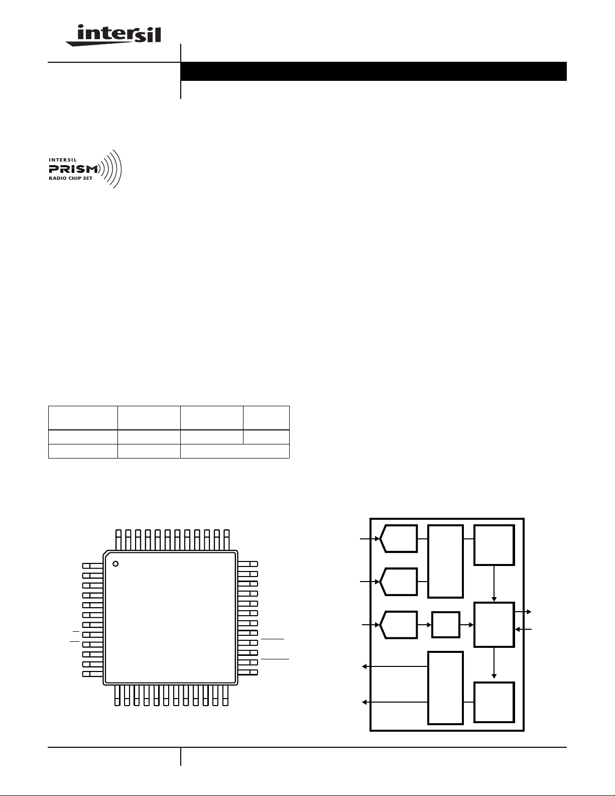
Simplified Block Diagram
I
Q
RSSI
I
OUT
IN
IN
3-BIT
A/D
3-BIT
A/D
6-BIT
A/D
DE-SPREADER
CCA
DEMOD.
PRO-
CESSOR
INTER-
FACE
DATA TO NETWORK
CTRL
PROCESSOR
Q
IN
Q
GND
REFP
RSSI
REFN
V
V
V
4-1
DD
DDA
GND
SDI
DDA
V
GND
V
SCLK
CAUTION: These devices are sensitive to electrostatic discharge; follow proper IC Handling Procedures.
http://www.intersil.com or 407-727-9207
PRISM® is a registered trademark of Intersil Corporation. PRISM logo is a trademark of Intersil Corporation.
OUT
SPREADER
| Copyright © Intersil Corporation 1999
MOD.
Page 2

HFA3860B
Table of Contents
PAGE
Ordering Information . . . . . . . . . . . . . . . . . . . . . . . . . . . . . . . . . . . . . . . . . . . . . . . . . . . . . . . . . . . . . . . . . . . . . . . . . . . . . . . . 1
Pinout. . . . . . . . . . . . . . . . . . . . . . . . . . . . . . . . . . . . . . . . . . . . . . . . . . . . . . . . . . . . . . . . . . . . . . . . . . . . . . . . . . . . . . . . . . . . 1
Simplified Block Diagram . . . . . . . . . . . . . . . . . . . . . . . . . . . . . . . . . . . . . . . . . . . . . . . . . . . . . . . . . . . . . . . . . . . . . . . . . . . . . 1
Typical Application Diagram. . . . . . . . . . . . . . . . . . . . . . . . . . . . . . . . . . . . . . . . . . . . . . . . . . . . . . . . . . . . . . . . . . . . . . . . . . . 3
Pin Descriptions . . . . . . . . . . . . . . . . . . . . . . . . . . . . . . . . . . . . . . . . . . . . . . . . . . . . . . . . . . . . . . . . . . . . . . . . . . . . . . . . . . . . 3
External Interfaces . . . . . . . . . . . . . . . . . . . . . . . . . . . . . . . . . . . . . . . . . . . . . . . . . . . . . . . . . . . . . . . . . . . . . . . . . . . . . . . . . . 5
Control Port (4 Wire) . . . . . . . . . . . . . . . . . . . . . . . . . . . . . . . . . . . . . . . . . . . . . . . . . . . . . . . . . . . . . . . . . . . . . . . . . . . . . . . . 5
TX Port. . . . . . . . . . . . . . . . . . . . . . . . . . . . . . . . . . . . . . . . . . . . . . . . . . . . . . . . . . . . . . . . . . . . . . . . . . . . . . . . . . . . . . . . . . . 7
RX Port. . . . . . . . . . . . . . . . . . . . . . . . . . . . . . . . . . . . . . . . . . . . . . . . . . . . . . . . . . . . . . . . . . . . . . . . . . . . . . . . . . . . . . . . . . . 8
I/Q A/D Interface. . . . . . . . . . . . . . . . . . . . . . . . . . . . . . . . . . . . . . . . . . . . . . . . . . . . . . . . . . . . . . . . . . . . . . . . . . . . . . . . . . . . 8
A/D Calibration Circuit and Registers. . . . . . . . . . . . . . . . . . . . . . . . . . . . . . . . . . . . . . . . . . . . . . . . . . . . . . . . . . . . . . . . . . . . 9
RSSI A/D Interface. . . . . . . . . . . . . . . . . . . . . . . . . . . . . . . . . . . . . . . . . . . . . . . . . . . . . . . . . . . . . . . . . . . . . . . . . . . . . . . . . . 10
Test Port. . . . . . . . . . . . . . . . . . . . . . . . . . . . . . . . . . . . . . . . . . . . . . . . . . . . . . . . . . . . . . . . . . . . . . . . . . . . . . . . . . . . . . . . . . 10
Definitions. . . . . . . . . . . . . . . . . . . . . . . . . . . . . . . . . . . . . . . . . . . . . . . . . . . . . . . . . . . . . . . . . . . . . . . . . . . . . . . . . . . . . . . . . 11
Power Down Modes. . . . . . . . . . . . . . . . . . . . . . . . . . . . . . . . . . . . . . . . . . . . . . . . . . . . . . . . . . . . . . . . . . . . . . . . . . . . . . . . . 12
Transmitter Description . . . . . . . . . . . . . . . . . . . . . . . . . . . . . . . . . . . . . . . . . . . . . . . . . . . . . . . . . . . . . . . . . . . . . . . . . . . . . . 12
Header/Packet Description. . . . . . . . . . . . . . . . . . . . . . . . . . . . . . . . . . . . . . . . . . . . . . . . . . . . . . . . . . . . . . . . . . . . . . . . . . . . 13
Scrambler and Data Encoder Description . . . . . . . . . . . . . . . . . . . . . . . . . . . . . . . . . . . . . . . . . . . . . . . . . . . . . . . . . . . . . . . . 14
Spread Spectrum Modulator Description . . . . . . . . . . . . . . . . . . . . . . . . . . . . . . . . . . . . . . . . . . . . . . . . . . . . . . . . . . . . . . . . . . . . 15
CCK Modulation. . . . . . . . . . . . . . . . . . . . . . . . . . . . . . . . . . . . . . . . . . . . . . . . . . . . . . . . . . . . . . . . . . . . . . . . . . . . . . . . . . . . 16
Clear Channel Assessment (CCA) and Energy Detect (ED) Description. . . . . . . . . . . . . . . . . . . . . . . . . . . . . . . . . . . . . . . . . 17
Demodulator Description . . . . . . . . . . . . . . . . . . . . . . . . . . . . . . . . . . . . . . . . . . . . . . . . . . . . . . . . . . . . . . . . . . . . . . . . . . . . . 18
Acquisition Description. . . . . . . . . . . . . . . . . . . . . . . . . . . . . . . . . . . . . . . . . . . . . . . . . . . . . . . . . . . . . . . . . . . . . . . . . . . . . . . 18
Two Antenna Acquisition (Recommended for Indoor Use) . . . . . . . . . . . . . . . . . . . . . . . . . . . . . . . . . . . . . . . . . . . . . . . . . . 18
One Antenna Acquisition (Only Recommended if Multipath is Not Significant). . . . . . . . . . . . . . . . . . . . . . . . . . . . . . . . . . . 19
Acquisition Signal Quality Parameters. . . . . . . . . . . . . . . . . . . . . . . . . . . . . . . . . . . . . . . . . . . . . . . . . . . . . . . . . . . . . . . . . . 19
Procedure to Set Acq. Signal Quality Parameters Example . . . . . . . . . . . . . . . . . . . . . . . . . . . . . . . . . . . . . . . . . . . . . . . . . 21
PN Correlators Description. . . . . . . . . . . . . . . . . . . . . . . . . . . . . . . . . . . . . . . . . . . . . . . . . . . . . . . . . . . . . . . . . . . . . . . . . . . . 21
Data Demodulation and Tracking Description (DBPSK and DQPSK Modes) . . . . . . . . . . . . . . . . . . . . . . . . . . . . . . . . . . . . . 22
Data Decoder and Descrambler Description . . . . . . . . . . . . . . . . . . . . . . . . . . . . . . . . . . . . . . . . . . . . . . . . . . . . . . . . . . . . . . . . . . . . 22
Data Demodulation Description (BMBOK and QMBOK Modes) . . . . . . . . . . . . . . . . . . . . . . . . . . . . . . . . . . . . . . . . . . . . . . . 23
Data Demodulation in the CCK Modes . . . . . . . . . . . . . . . . . . . . . . . . . . . . . . . . . . . . . . . . . . . . . . . . . . . . . . . . . . . . . . . . . . 23
Tracking . . . . . . . . . . . . . . . . . . . . . . . . . . . . . . . . . . . . . . . . . . . . . . . . . . . . . . . . . . . . . . . . . . . . . . . . . . . . . . . . . . . . . . . . . . 25
Demodulator Performance. . . . . . . . . . . . . . . . . . . . . . . . . . . . . . . . . . . . . . . . . . . . . . . . . . . . . . . . . . . . . . . . . . . . . . . . . . . . 25
Overall Eb/N0 Versus BER Performance . . . . . . . . . . . . . . . . . . . . . . . . . . . . . . . . . . . . . . . . . . . . . . . . . . . . . . . . . . . . . . . 25
Clock Offset Tracking Performance. . . . . . . . . . . . . . . . . . . . . . . . . . . . . . . . . . . . . . . . . . . . . . . . . . . . . . . . . . . . . . . . . . . . 26
Carrier Offset Frequency Performance . . . . . . . . . . . . . . . . . . . . . . . . . . . . . . . . . . . . . . . . . . . . . . . . . . . . . . . . . . . . . . . . . 26
A Default Register Configuration . . . . . . . . . . . . . . . . . . . . . . . . . . . . . . . . . . . . . . . . . . . . . . . . . . . . . . . . . . . . . . . . . . . . . . . 27
Control Registers . . . . . . . . . . . . . . . . . . . . . . . . . . . . . . . . . . . . . . . . . . . . . . . . . . . . . . . . . . . . . . . . . . . . . . . . . . . . . . . . . . . 28
Test Circuit. . . . . . . . . . . . . . . . . . . . . . . . . . . . . . . . . . . . . . . . . . . . . . . . . . . . . . . . . . . . . . . . . . . . . . . . . . . . . . . . . . . . . . . . 38
Thin Plastic Quad Flatpack Packages (TQFP). . . . . . . . . . . . . . . . . . . . . . . . . . . . . . . . . . . . . . . . . . . . . . . . . . . . . . . . . . . . . 40
4-2
Page 3
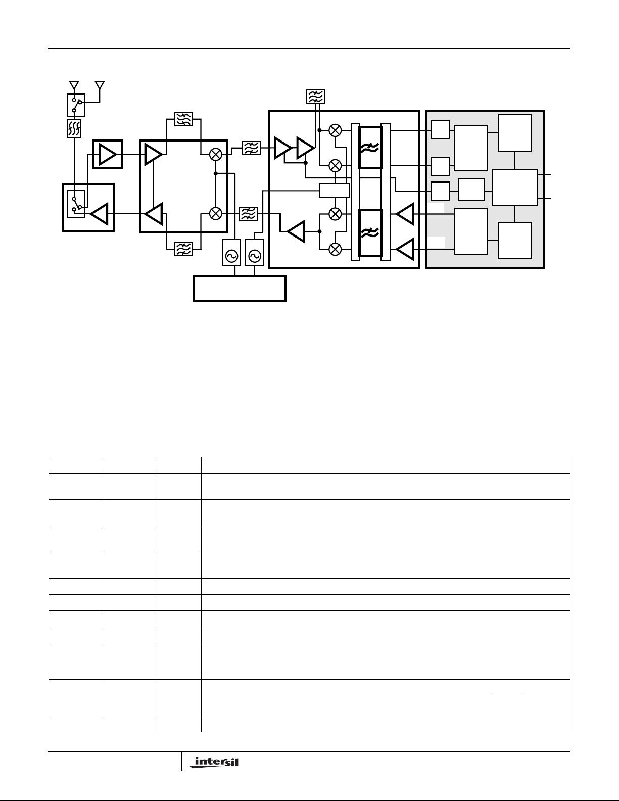
Typical Application Diagram
HFA3860B
HF A3424(NOTE)
(FILE# 4131)
HF A3624
UP/DOWN
CONVERTER
(FILE# 4066)
RFPA
HF A3925
(FILE# 4132)
TYPICAL TRANSCEIVER APPLICATION CIRCUIT USING THE HFA3860B
NOTE: Required for systems targeting 802.11 specifications.
VCO
VCO
DUAL SYNTHESIZER
HFA3524
(FILE# 4062)
÷2
0o/90
QUAD IF MODULATOR
HFA3724/6
(FILE# 4067)
I
M
o
U
X
Q
HF A3860B
(FILE# 4594)
RXI
RXQ
RSSI
M
U
X
A/D
DE-
SPREAD
A/D
CCA
A/D
TXI
SPREAD
TXQ
DSSS BASEBAND PROCESSOR
DEMOD
802.11
MAC-PHY
INTERFACE
MOD.
DATA TO MACCTRL
For additional information on the PRISM™ chip set, call
(407) 724-7800 to access Harris’ AnswerFAX system. When
prompted, key in the four-digit document number (File #) of
The four-digit file numbers are shown in the Typical
Application Diagram, and correspond to the appropriate
circuit.
the data sheets you wish to receive.
Pin Descriptions
NAME PIN TYPE I/O DESCRIPTION
V
DDA
(Analog)
V
DD
(Digital)
GND
(Analog)
GND
(Digital)
V
REFN
V
REFP
I
IN
Q
IN
ANTSEL 26 O The antenna select signal changes state as the receiver switches from antenna to antenna during the
ANTSEL 27 O The antenna select signal changes state as the receiver switches from antenna to antenna during the
RSSI 14 I Receive Signal Strength Indicator Analog input.
10, 18, 20 Power DC power supply 2.7V - 3.6V (Not Hardwired Together On Chip).
7, 21, 29, 42 Power DC power supply 2.7 - 3.6V
11, 15, 19 Ground DC power supply 2.7 - 3.6V, ground (Not Hardwired Together On Chip).
6, 22, 31, 41 Ground DC power supply 2.7 - 3.6V, ground.
17 I “Negative” voltage reference for A/D’s (I and Q) [Relative to V
REFP
]
16 I “Positive” voltage reference for A/D’s (I, Q and RSSI)
12 I Analog input to the internal 3-bit A/D of the In-phase received data.
13 I Analog input to the internal 3-bit A/D of the Quadrature received data.
acquisition process in the antenna diversity mode. This is a complement for ANTSEL (pin 27) for
differential drive of antenna switches.
acquisition process in the antenna diversity mode. This is a complement for ANTSEL (pin 26) for
differential drive of antenna switches.
4-3
Page 4

HFA3860B
Pin Descriptions
NAME PIN TYPE I/O DESCRIPTION
TX_PE 2 I When active, the transmitter is configured to be operational, otherwise the transmitter is in standby
TXD 3 I TXD is an input, used to transfer MAC Payload Data Unit (MPDU) data from the MAC or network
TXCLK 4 O TXCLK is a clock output used to receive the data on the TXD from the MAC or network processor to
TX_RDY 5 O TX_RDY is an output to the external network processor indicating that Preamble and Header
CCA 32 O ClearChannelAssessment (CCA) is an output used to signal that the channel is clear to transmit. The
RXD 35 O RXD is an output to the external network processor transferring demodulated Header information and
RXCLK 36 O RXCLK is the bit clock output. This clock is used to transfer Header information and payload data
MD_RDY 34 O MD_RDY is an output signal to the network processor, indicating header data and a data packet are
RX_PE 33 I When active, the receiver is configured to be operational, otherwise the receiver is in standby mode.
SD 25 I/O SD is a serial bidirectional data bus which is used to transfer address and data to/from the internal
SCLK 24 I SCLK is the clock for the SD serial bus. The data on SD is clocked at the rising edge. SCLK is an input
SDI 23 I Serial Data Input in 3 wire mode described in Tech Brief 362. This pin is not used in the 4 wire interface
R/W8 IR/W is an input to the HFA3860B used to change the direction of the SD bus when reading or writing
CS 9 I CS is a Chip select for the device to activate the serial control port. The CS doesn’t impact any of the
TEST 7:0 37, 38, 39,
40, 43, 44,
45, 46
(Continued)
mode. TX_PE isaninputfromthe external Media Access Controller (MAC) or network processortothe
HFA3860B. The rising edge of TX_PE will start the internal transmit state machine and the falling edge
will initiate shut down of the state machine. TX_PE envelopes the transmit data except for the last bit.
The transmitterwill continue to runfor3 symbols afterTX_PEgoes inactive toallowthe PAtoshut down
gracefully.
processor to the HFA3860B. The data is received serially with the LSB first. The data is clocked in the
HFA3860B at the rising edge of TXCLK.
the HFA3860B, synchronously. Transmit data on the TXD bus is clocked into the HFA3860B on the
rising edge. The clocking edge is also programmabletobeoneitherphaseoftheclock.Therateof the
clock will be dependent upon the data rate that is programmed in the signalling field of the header.
information has been generated and that the HFA3860B is ready to receive the data packet from the
network processorover theTXDserial bus.The TX_RDYreturns totheinactive state whenthelastchip
of the last symbol has been output.
CCA algorithm makesits decision as a function ofRSSI,Energy detect (ED), and Carrier Sense(CRS).
The CCA algorithm and its features are described elsewhere in the data sheet.
Logic 0 = Channel is clear to transmit.
Logic 1 = Channel is NOT clear to transmit (busy).
This polarity is programmable and can be inverted.
data in a serial format. The data is sent serially with the LSB first. The data is frame aligned with
MD_RDY.
through the RXD serial bus to the network processor. This clock reflects the bit rate in use. RXCLK is
held to a logic “0” state during the CRC16 reception. RXCLK becomes active after the SFD has been
detected. Data should be sampled on the rising edge. This polarity is programmable and can be
inverted.
ready to be transferred to the processor. MD_RDY is an active high signal and it envelopes the data
transfer over the RXD serial bus. MD_RDY goes active when the SFD is detected and returns to its
inactive state when RX_PE goes inactive or an error is detected in the header.
This is an active high input signal. In standby, RX_PE inactive, all A/D converters are disabled.
registers. The bit ordering of an 8-bit word is MSB first. The first 8 bits during transfers indicate the
register address immediately followed by 8 more bits representing the data that needs to be written or
read at that register.
clock and it is asynchronous to the internal master clock (MCLK)The maximum rate of this clock is
11MHz or one half the master clock frequency, whichever is lower.
described in this data sheet. It should not be left floating.
data on the SD bus.R/W alsoenablestheserialshiftregisterusedinareadcycle.R/Wmustbe set up
prior to the rising edge of SCLK. A high level indicates read while a low level is a write.
other interface ports and signals, i.e., the TX or RX ports and interface signals. This is an active low
signal. When inactive SD, SCLK, and R/W become “don’t care” signals.
O This is a data port that can be programmed to bring out internal signals or data for monitoring. These
bits are primarily reserved by the manufacturerfor testing. A further description of the test port is given
at the appropriate section of this data sheet.
4-4
Page 5

HFA3860B
Pin Descriptions
NAME PIN TYPE I/O DESCRIPTION
TEST_CK 1 O This is the clock that is used in conjunction with the data that is being output from the test bus (TEST
RESET 28 I Master reset for device. When active TX and RX functions are disabled. If RESET is kept low the
MCLK 30 I Master Clock for device. The nominal frequency of this clock is 44MHz. This is used internally to
I
OUT
Q
OUT
NOTE: Total of 48 pins; ALL pins are used.
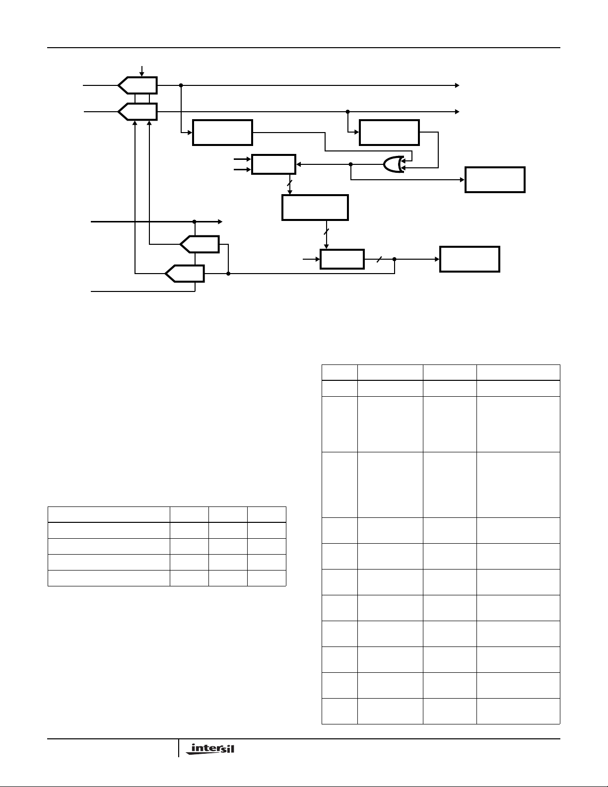
External Interfaces
There are three primary digital interface ports for the
HFA3860B that are used for configuration and during normal
operation of the device as shown in Figure 1. These ports are:
• The Control Port, which is used to configure, write
and/or read the status of the internal HFA3860B
registers.
• The TX Port, which is used to accept the data that
needs to be transmitted from the network processor.
• The RX Port, which is used to output the received
demodulated data to the network processor.
In addition to these primary digital interfaces the device
includes a byte wide parallel Test Port which can be
configured to output various internal signals and/or data.
The device can also be set into various power consumption
modes by external control. The HFA3860B contains three
Analog to Digital (A/D) converters. The analog interfaces to
the HFA3860B include, the In phase (I) and Quadrature (Q)
data component inputs, and the RF signal strength indicator
input. A reference voltage divider is also required external to
the device.
(Continued)
0-7).
HFA3860Bgoes into the power standby mode. RESET does not alter any of the configuration register
values nor does it preset any of the registers into default values. Device requires programming upon
power-up.
generate all other internal necessary clocks and is divided by 2 or 4 for the transceiver clocks.
48 O TX Spread baseband I digital output data. Data is output at the chip rate.
47 O TX Spread baseband Q digital output data. Data is output at the chip rate.
Control Port (4 Wire)
The serial control port is used to serially write and read data
to/from the device. This serial port can operate up to a
11MHz rate or 1/2 the maximum master clock rate of the
device, MCLK (whichever is lower). MCLK must be running
during programming. This port is used to program and to
read all internal registers. The first 8 bits always represent
the address followed immediately by the 8 data bits for that
register. The two LSBs of address are don’t care, but
reserved for future expansion. The serial transfers are
accomplished through the serial data pin (SD). SD is a
bidirectional serial data bus. Chip Select (
Read/
Write (R/W) are also required as handshake signals
for this port. The clock used in conjunction with the address
and data on SD is SCLK. This clock is provided by the
external source and it is an input to the HFA3860B. The
timing relationships of these signals are illustrated in
Figures 2 and 3. R/
low when it is to be wr itten.
the state machine.
entire data transfer cycle.
device only. The serial control port operates
asynchronously from the TX and RX ports and it can
W is high when data is to be read, and
CS is an asynchronous reset to
CS must be active (low) during the
CS selects the serial control por t
CS), and
accomplish data transfers independent of the activity at the
ANTSEL
ANTSEL
ANALOG
INPUTS
REFERENCE
A/D
POWER
DOWN
SIGNALS
TEST
PORT
TESTCK
HFA3860B
I (ANALOG)
Q (ANALOG)
RSSI (ANALOG)
V
REFN
V
REFP
TX_PE
RX_PE
RESET
9
TEST
TXD
TXCLK
TX_RDY
RXD
RXCLK
MD_RDY
CS
SD
SCLK
R/
SDI
I
Q
W
TX OUTPUTS
TX_PORT
RX_PORT
CONTROL_PORT
other digital or analog ports.
The HFA3860B has 34 internal registers that can be
configured through the control port. These registers are
listed in the Configuration and Control Internal Register
table. Table 1 lists the configuration register number, a brief
name describing the register, and the HEX address to
access each of the registers. The type indicates whether the
corresponding register is Read only (R) or Read/Write
(R/W). Some registers are two bytes wide as indicated on
the table (high and low bytes). To fully program the
HFA3860B registers requires two writes of registers CR16
and CR17. This shadow register scheme extends the
register compliment by two registers from 32 to 34 without
FIGURE 1. EXTERNAL INTERFACE
requiring an additional address bit.
4-5
Page 6
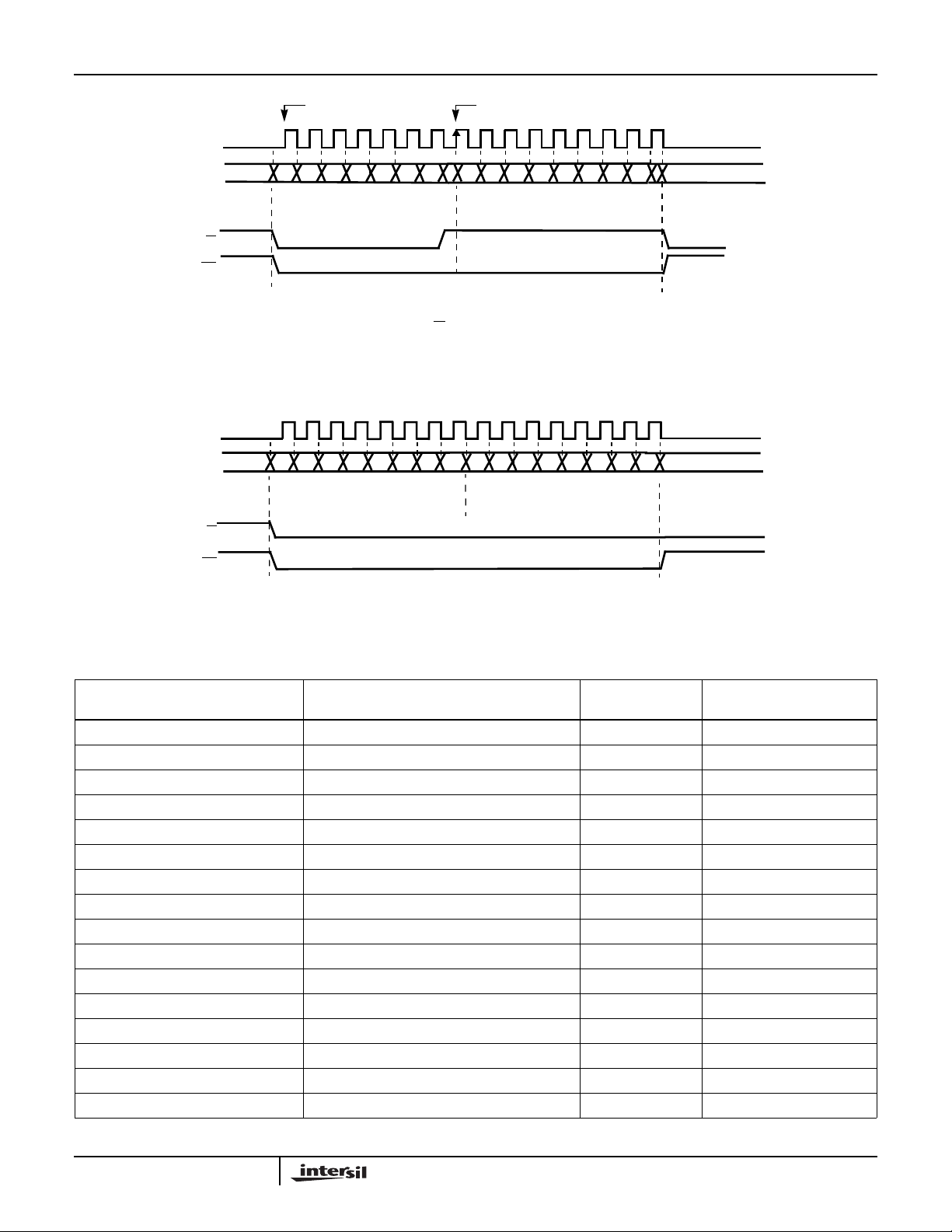
SCLK
HFA3860B
FIRST ADDRESS BIT FIRST DATABIT OUT
7654321076543210
SD
R/
W
CS
1234567 01234567
LSBDATA OUTMSBMSB ADDRESS IN
NOTES:
1. The HFA3860B always uses the rising edge of SCLK. SD, R/W and CS hold times allow the controller to use either the rising or falling edge.
2. This port operates essentially the same as the HFA3824 with the exception that the AS signal of the 3824 is not required.
FIGURE 2. CONTROL PORT READ TIMING
SCLK
SD
R/
CS
W
7654321076543210
1234567 012345670
LSBDATA INMSBMSB ADDRESS IN
FIGURE 3. CONTROL PORT WRITE TIMING
TABLE 1. CONFIGURATION AND CONTROL INTERNAL REGISTER LIST
CONFIGURATION
REGISTER NAME TYPE
CR0 Part/Version Code R 00
CR1 I/O Polarity R/W 04
CR2 TX and RX Control R/W 08
CR3 A/D_CAL_POS Register R/W 0C
CR4 A/D_CAL_NEG Register R/W 10
CR5 CCA Antenna Control R/W 14
CR6 Preamble Length R/W 18
CR7 Scramble_Tap (RX and TX) R/W 1C
CR8 RX_SQ1_ ACQ (High) Threshold R/W 20
CR9 RX-SQ1_ ACQ (Low) Threshold R/W 24
CR10 RX_SQ2_ ACQ (High) Threshold R/W 28
CR11 RX-SQ2_ ACQ (Low) Threshold R/W 2C
CR12 SQ1 CCA Thresh (High) R/W 30
CR13 SQ1 CCA Thresh (Low) R/W 34
CR14 ED or RSSI Thresh R/W 38
CR15 SFD Timer R/W 3C
REGISTER
ADDRESS HEX
4-6
Page 7

HFA3860B
TABLE 1. CONFIGURATION AND CONTROL INTERNAL REGISTER LIST (Continued)
CONFIGURATION
REGISTER NAME TYPE
CR16 (Note 3) Signal Field (BPSK - 11 Chip Sequence)
or (Cover Code (Low))
CR17 (Note 3) Signal Field (QPSK - 11 Chip Sequence)
or (Cover Code (High))
CR18 Signal Field (BPSK - Mod. Walsh Sequence)
or (CCK 5.5Mbps)
CR19 Signal Field (QPSK - Mod. Walsh Sequence)
or (CCK 11Mbps)
CR20 TX Signal Field R/W 50
CR21 TX Service Field R/W 54
CR22 TX Length Field (High) R/W 58
CR23 TX Length Field (Low) R/W 5C
CR24 RX Status R 60
CR25 RX Service Field Status R 64
CR26 RX Length Field Status (High) R 68
CR27 RX Length Field Status (Low) R 6C
CR28 Test Bus Address R/W 70
CR29 Test Bus Monitor R 74
CR30 Test Register 1, Must Load 00H R/W 78
CR31 RX Control R/W 7C
NOTE:
3. To provide CCK functionality, these registers must be programmed in two passes. Once with CR5 bit 7 as a 0 and once with it as a 1.
R/W 40
R/W 44
R/W 48
R/W 4C
REGISTER
ADDRESS HEX
TX Port
The transmit data port accepts the data that needs to be
transmitted serially from an external data source. The data is
modulated and transmitted as soon as it is received from the
external data source.TheserialdataisinputtotheHFA3860B
through TXD using the next rising edge of TXCLK to clock it in
the HF A3860B. TXCLK is an output from the HFA3860B. A
timing scenario of the transmit signal handshakes and
sequence is shown on timing diagram Figure 4.
The external processor initiates the transmit sequence by
asserting TX_PE. TX_PE envelopes the transmit data packet
on TXD. The HFA3860B responds by generating a Preamble
and Header. Bef ore the last bit of the Header is sent, the
HF A3860B begins gener ating TXCLK to input the serial data
on TXD. TXCLK will run until TX_PE goes bac k to its inactive
state indicating the end of the data packet. The user needs to
hold TX_PE high for as many clocks as there bits to transmit.
For the higher data rates, this will be in multiples of the
number of bits per symbol. The HFA3860B will continue to
output modulated signal for 2µs after the last data bit is
output, to supply bits to flush the modulation path. TX_PE
must be held until the last data bit is output from the
MAC/FIFO. The minim um TX_PE inactive pulse required to
restart the preamble and header generation is 2.22µs and to
reset the modulator is 4.22µs.
The HFA3860Binternallygeneratesthepreambleandheader
information from information supplied via the control registers.
The external source needs to provide only the data portion of
the packetand set the control registers. The timing diagram of
this process is illustrated on Figure 4. Assertion of TX_PE will
initialize the generation of the preamble and header.TX_RDY,
which is an output from the HF A3860B, is used to indicate to
the external processor that the preamble has been generated
and the device is ready to receive the data packet (MPDU) to
be transmitted from the external processor. Signals TX_RDY,
TX_PE and TXCLK can be set individually, by programming
Configuration Register (CR) 1, as either active high or active
low signals.
The transmit port is completely independent from the
operation of the other interface ports including the RX port,
therefore supporting a full duplex mode.
4-7
Page 8
TXCLK
HFA3860B
TX_PE
TXD
TX_RDY
NOTE: Preamble/Header and Data is transmitted LSB first. TXD shown generated from rising edge of TXCLK.
RXCLK
RX_PE
HEADER
FIELDS
PROCESSING
MD_RDY
RXD
PREAMBLE/HEADER
FIRST DATA BIT SAMPLED
LSB DATA PACKET
FIGURE 4. TX PORT TIMING
LSB DATA PACKET MSB
MSB
DAT A
LAST DATA BIT SAMPLED
DEASSERTED WHEN LAST
CHIP OF MPDU CLEARS
MOD PATH OF 3860
NOTE: MD_RDY active after CRC16. See detailed timing diagrams (see Figures 22, 23, 24).
FIGURE 5. RX PORT TIMING
RX Port
The timing diagram Figure 5 illustrates the relationships
between the various signals of the RX port. The receive data
port serially outputs the demodulated data from RXD. The
data is output as soon as it is demodulated by the
HFA3860B.RX_PE mustbe at its activestate throughout the
receive operation. When RX_PE is inactive the device's
receive functions, including acquisition, will be in a stand by
mode.
RXCLK is an output from the HFA3860Bandis the clock for
the serial demodulated data on RXD.MD_RDY is an output
from the HFA3860B and it may be set to go active after
SFD or CRC fields. Note that RXCLK becomes active after
the Start Frame Delimiter (SFD) to clock out the Signal,
Service, and Length fields, then goes inactive during the
header CRC field. RXCLK becomes active again for the
data. MD_RDY returns to its inactive state after RX_PE is
deactivated by the external controller, or if a header error is
detected. A header error is either a failure of the CRC
check, or the failure of the received signal field to match
one of the 4 programmed signal fields. For either type of
header error, the HFA3860B will reset itself after reception
of the CRC field. If MD_RDY had been set to go active after
CRC, it will remain low.
MD_RDYandRXCLKcanbeconfiguredthroughCR1,bit6-7
to be active low,or active high. The receive port is completely
independent from the operation of the other interface ports
including the TX port, supporting therefore a full duplex mode.
I/Q A/D Interface
The PRISM baseband processor chip (HFA3860B) includes
two 3-bit Analog to Digital converters (A/Ds) that sample the
analog input from the IF down converter. The I/Q A/D clock,
samples at twice the chip rate. The nominal sampling rate is
22MHz.
The interface specifications for the I and Q A/Ds are listed in
Table 2.
4-8
Page 9

HFA3860B
TABLE 2. I, Q, A/D SPECIFICATIONS
PARAMETER MIN TYP MAX
Full Scale Input Voltage (V
Input Bandwidth (-0.5dB) - 20MHz Input Capacitance (pF) - 5 Input Impedance (DC) 5kΩ -FS (Sampling Frequency) - 22MHz -
The voltages applied to pin 16, V
) 0.25 0.50 1.0
P-P
and pin 17, V
REFP
REFN
set the references for the internal I and Q A/D converters. In
addition, V
reference. For a nominal I/Q input of 500mV
suggested V
V
is 0.86V. V
REFN
is also used to set the RSSI A/D converter
REFP
voltage is 1.75V, and the suggested
REFP
should never be less than 0.25V.
REFN
P-P
, the
Figure 6 illustrates the suggested interface configuration for
the A/Ds and the reference circuits.
Since these A/Ds are intended to sample AC voltages, their
inputs are biased internally and they should be capacitively
coupled. The HPF corner frequency in the baseband receive
path should be less than 1kHz.
.
I
IN
Q
IN
V
REFP
V
REFN
HFA3860B
2V
I
Q
3.9K
0.15µF
0.15µF
8.2K
9.1K
FIGURE 6. INTERFACES
0.01µF
0.01µF
The A/D section includes a compensation (calibration) circuit
that automatically adjusts for temperature and component
variations of the RF and IF strips. The variations in gain of
limiters, AGC circuits, filters etc. can be compensated for up
to ±4dB. Without the compensation circuit, the A/Ds could
see a loss of up to 1.5 bits of the 3 bits of quantization. The
A/D calibration circuit adjusts the A/D reference voltages to
maintain optimum quantization of the IF input over this
variation range. It works on the principle of setting the
reference to insure that the signal is at full scale (saturation)
a certain percentage of the time. Note that this is not an
AGC and it will compensate only for slow variations in signal
levels (several seconds).
The procedure for setting the A/D references to
accommodate various input signal voltage levels is to set the
reference voltages so that the A/D calibration circuit is
operating at half scale with the nominal input. This leaves
the maximum amount of adjustment room for circuit
tolerances.
A/D Calibration Circuit and Registers
The A/D compensation or calibration circuit is designed to
optimize A/D performance for the I and Q inputs by
maintaining the full 3-bit resolution of the outputs. There are
two registers (CR 3 AD_CAL_POS and CR 4
AD_CAL_NEG) that set the parameters for the internal I and
Q A/D calibration circuit.
Both I and Q A/D outputs are monitored by the A/D
calibration circuit as shown in Figure 7 and if either has a full
scale value, a 24-bit accumulator is incremented as defined
by parameter AD_CAL_POS. If neither has a full scale
value, the accumulator is decremented as defined by
parameter AD_CAL_NEG. The output of this accumulator is
used to drive D/A converters that adjust the A/D’s
references. Loop gain reduction is accomplished by using
only the 5 MSBs out of the 24 bits. The compensation
adjustment is updated at a 1kHz rate. The A/D calibration
circuit is only intended to remove slow component variations.
Forbest performance,the optimum probability that either the
I or Q A/D converter is at the saturation level was determined
to be 50%. The probability P is set by the formula:
P(AD_CAL_POS)+(1-P)(AD_CAL_NEG) = 0.
One solution to this formula for P = 1/2 is:
AD_CAL_POS = 1
AD_CAL_NEG = -1
This also sets the levels so that operation with either NOISE
or SIGNAL is approximately the same. It is assumed that the
RF and IF sections of the receiver have enough gain to
cause limiting on thermal noise. This will keep the levels at
the A/D approximately the same regardless of whether
signal is present or not. The A/D calibration is normally set to
work only while the receiver is tracking, but it can be set to
operate all the time the receiver is on or it can be turned off
and held at mid scale.
The A/D calibration circuit operation can be defined through
CR 2, bits 3 and 4. Table 3 illustrates the possible
configurations. The A/D Cal function should initially be
programmed for mid scale operation to preset it, then
programmedforeithertrackingmode.Thisinitializesthepart
for most rapid settling on the appropriate values.
TABLE 3. A/D CALIBRATION
CR 2
BIT 4
0 0 OFF, Reference set at mid scale.
0 1 OFF, Reference set at mid scale.
1 0 A/D_Cal while tracking only.
1 1 A/D_Cal while RX_PE active.
CR 2
BIT 3
A/D CALIBRATION CIRCUIT
CONFIGURATION
4-9
Page 10
RX_I_IN
RX_Q_IN
A/D
A/D
A/D_CK
/
3
HFA3860B
/
3
+FS OR -FS
COMPARE
+FS OR -FS
COMPARE
TO CORRELATOR
/
8
/
8
TO RSSI A/D
A/D_CAL_CK
(APPROX 1KHz)
SELECT
V
REFN
ANALOG
BIASES
V
REFP
A/D_CAL_POS
A/D_CAL_NEG
D/A
D/A
FIGURE 7. A/D CAL CIRCUIT
RSSI A/D Interface
The Receive Signal Strength Indication (RSSI) analog signal is
input to a 6-bit A/D, indicating 64 discrete levels of received
signal strength. This A/D measures a DC voltage, so its input
must be DC coupled. Pin 16 (V
RSSI A/D converter. V
is common for the I and Q and
REFP
) sets the reference for the
REFP
RSSI A/Ds. The RSSI signal is used as an input to the Clear
Channel Assessment (CCA) algorithm of the HFA3860B . The
RSSI A/D output is stored in an 6-bit register available via the
TEST Bus and the TEST Bus monitor register. CCA is further
described on page 17.
The interface specifications for the RSSI A/D are listed in
Table 4 below (V
TABLE 4. RSSI A/D SPECIFICATIONS
PARAMETER MIN TYP MAX
Full Scale Input Voltage - - 1.15
Input Bandwidth (0.5dB) 1MHz - Input Capacitance - 7pF Input Impedance (DC) 1M - -
REFP
= 1.75V).
Test Port
The HFA3860B provides the capability to access a number of
internal signals and/or data through the Test port, pins TEST
7:0. In addition pin 1 (TEST_CK) is an output that can be used
in conjunction with the data coming from the test port outputs.
The test port is programmable through configuration register
(CR28). Any signal on the test port can also be read from
configuration register (CR29) via the serial control port.
8
ACCUMULATOR
(25-BIT)
5 MSBs
There are 32 modes assigned to the PRISM test port. Some
are only applicable to factory test.
MODE DESCRIPTION TEST_CLK TEST (7:0)
(0Ah)
TEST REG
MODE 1 (7)
A/DCAL
A/D_CAL_ACCUM
(1/4 dB PER LSB)
REG
5
TEST REG
MODE 25 (8:0)
TABLE 5. TEST MODES
0 Quiet Test Bus 0 00
1 RX Acquisition
Monitor
Initial Detect A/DCal, CRS, ED,
Track, SFD Detect,
Signal Field Ready,
Length Field Ready,
Header CRC Valid
2 TX Field Monitor IQMARK A/DCal, TXPE Inter-
nal, Preamble Start,
SFD Start, Signal
Field Start, Length
FieldStart, CRCStart,
MPDU Start
3 RSSI Monitor RSSI Pulse CSE Latched, CSE,
RSSI Out (5:0)
4 SQ1 Monitor Pulse after
SQ1 (7:0)
SQ is valid
5 SQ2 Monitor Pulse after
SQ2 (7:0)
SQ is valid
6 Correlator Lo
Rate
7 Freq Test Lo
Rate
8 Phase Test Lo
Rate
9 NCO Test Lo
Rate
10
Bit Sync Accum
Lo Rate
Sample CLK Correlator Magnitude
(7:0)
Subsample
CLK
Subsample
CLK
Subsample
Frequency Register
(18:11)
Phase Register (7:3)
Shift <2:0>
NCO Register (15:8)
CLK
Enable Bit Sync Accum (7:3)
Shift (2:0)
4-10
Page 11

HFA3860B
TABLE 5. TEST MODES (Continued)
MODE DESCRIPTION TEST_CLK TEST (7:0)
11 Reserved Reserved Factory Test Only
12 A/D Cal Test
Mode
13 Correlator IHigh
Rate
14 Correlator Q
High Rate
15 Chip Error
Accumulator
16 NCO Test Hi
Rate
17 Freq Test Hi
Rate
18 Carrier Phase
Error Hi Rate
19 Reserved Sample CLK Factory Test Only
20 Reserved Sample CLK Factory Test Only
21 I_A/D, Q_A/D Sample CLK 0,0,I_A/D(2:0),Q_A/D
22 Reserved Reserved Factory Test Only
23 Reserved Reserved Factory Test Only
24 Reserved Reserved Factory Test Only
25 A/D Cal AccumLoA/D Cal
26 A/D Cal AccumHiA/D Cal
27 Freq Accum Lo Freq Accum
28 Reserved Reserved Factory Test Only
29 SQ2 Monitor Hi Pulse After
30-31 Reserved Reserved Factory Test Only
A/D Cal CLK A/DCal, ED, A/DCal
Disable, ADCal (4:0)
Sample CLK Correlator I (8:1)/
CCK Magnitude
Sample CLK Correlator Q
(8:1)/CCK Quality
0 Chip Error Accum
(14:7)
Sample CLK NCO Accum (19:12)
Sample CLK Lag Accum (18:11)
Sample CLK Carrier Phase Error
(6,6:0)
(2:0)
A/D Cal Accum (7:0)
Accum (8)
A/D Cal Accum (16:9)
Accum (17)
Freq Accum (14:7)
(15)
SQ2 (15:8)
SQ Valid
Definitions
ED. Energy Detect, indicates that the RSSI value exceedsits
programmed threshold.
CRS. Carrier Sense, indicates that a signal has been
acquired (PN acquisition).
TXCLK. Transmit clock.
Track. Indicates start of tracking and start of SFD time-out.
SFD Detect. Variable time after track starts.
Signal Field Ready. ~ 8µs after SFD detect.
Length Field Ready. ~ 32µs after SFD detect.
Header CRC Valid. ~ 48µs after SFD detect.
DCLK. Data bit clock.
FrqReg. Contents of the NCO frequency register.
PhaseReg. Phase of signal after carrier loop correction.
NCO PhaseAccumReg. Contents of the NCO phase
accumulation register.
SQ1. Signal Quality measure #1. Contents of the bit sync
accumulator.Eight MSBs of most recent 16-bit stored value.
SQ2. Signal Quality measure #2. Signal phase variance
after removal of data. Eight MSBs of most recent 16-bit
stored value.
Sample CLK. Receive clock (RX sample clock). Nominally
22MHz.
Subsample CLK. LO rate symbol clock. Nominally 1MHz.
BitSyncAccum. Real time monitor of the bit synchronization
accumulator contents, mantissa only.
A/D_Cal_ck. Clock for applying A/D calibration corrections.
A/DCal. 5-bit value that drives the D/A adjusting the A/D
reference.
TABLE 6. POWER DOWN MODES
MODE RX_PE TX_PE RESET AT 44MHz DEVICE STATE
SLEEP Inactive Inactive Active 600µA Both transmit and receive functions disabled. Device in sleep mode. Control
Interface is stillactive. Register values aremaintained.Devicewill return to its
active state within 10µs plus settling time of AC coupling capacitors (about
5ms).
STANDBY Inactive Inactive Inactive 7mA Both transmit and receive operations disabled. Device will resume its
operational state within 1µs of RX_PE or TX_PE going active.
TX Inactive Active Inactive 10mA Receiver operations disabled. Receiver will return in its operational state
within 1µs of RX_PE going active.
RX Active Inactive Inactive 29mA Transmitter operations disabled. Transmitterwill return to its operational state
within 2 MCLKs of TX_PE going active.
NO CLOCK ICC Standby Active 300µA All inputs at VCC or GND.
4-11
Page 12

HFA3860B
Power Down Modes
The power consumption modes of the HFA3860B are
controlled by the following control signals.
Receiver PowerEnable (RX_PE, pin 33), which disables the
receiver when inactive.
Transmitter PowerEnable(TX_PE,pin2),whichdisablesthe
transmitter when inactive.
Reset (
RESET, pin 28), which puts the receiver in a sleep
mode. The power down mode where, both
RX_PE are used is the lowest possible power consumption
mode for the receiver. Exiting this mode requires a maximum
of 10µs before the device is back at its operational mode for
transmitters. Add 5ms more to be operational for receive
mode. It also requires that RX_PE be activated briefly to
clock in the change of state.
The contents of the Configuration Registers are not effected
by any of the power down modes. The external processor
does have access and can modify any of the CRs during the
power down modes. No reconfiguration is required when
returning to operational modes.
Table 6 describes the power down modes available for the
HFA3860B (V
other inputs to the part (MCLK, SCLK, etc.) continue to run
except as noted.
= 3.3V). The table values assume that all
CC
RESET and
Transmitter Description
The HFA3860B transmitter is designed as a Direct
Sequence Spread Spectrum Phase Shift Keying (DSSS
PSK) modulator. It can handle data rates of up to 11MBPS
(refer to AC and DC specifications). Two different
modulations are available for the 5.5Mbps and 11Mbps
modes. This is to accommodate backwards compatibility
with the HFA3860A and to provide an IEEE 802.11
standards compliant mode. The various modes of the
modulator are Differential Binary Phase Shift Keying
(DBPSK) for 1Mbps, Differential Quaternary Phase Shift
Keying (DQPSK) for 2Mbps, Binary M-ary Bi-Orthogonal
Keying(BMBOK) or Complementary Code Keying (CCK) for
5.5Mbps, and Quaternary M-ary Bi-Orthogonal Keying
(QMBOK) or CCK for 11Mbps. These implement data rates
as shown in Table 7. The major functional blocks of the
transmitter include a network processor interface, DPSK
modulator, high rate modulator, a data scrambler and a
spreader, as shown on Figure 11. A description of (M-ARY)
Bi-Orthogonal Keying can be found in Chapter 5 of:
“Telecommunications System Engineering”, by Lindsey and
Simon, Prentis Hall publishing. CCK is essentially a
quadraphase form of that modulation.
The preamble and header are alwaystransmittedas DBPSK
waveforms while the data packets can be configured to be
either DBPSK, DQPSK, BMBOK, QMBOK, or CCK. The
preamble is used by the receiver to achieve initial PN
synchronization while the header includes the necessary
data fields of the communications protocol to establish the
physical layer link. The transmitter generates the
synchronization preamble and header and knows when to
make the DBPSK to DQPSK or B/QMBOK or CCK
switchover, as required.
For the 1 and 2Mbps modes, the transmitter accepts data
from the external source, scrambles it, differentially encodes
it as either DBPSK or DQPSK, and mixes it with the BPSK
PN spreading. The baseband digital signals are then output
to the external IF modulator.
For the MBOK modes, the transmitter inputs the data and
forms it into nibbles (4 bits). At 5.5Mbps, it selects one of 8
spread sequences from a table of sequences with 3 of those
bits and then picks the true or inverted version of that
sequence with the remaining bit. Thus, there are 16 possible
spread sequences to send, but only one is sent. This
sequence is then modulated on both the I and Q outputs.
The phase of the last bit of the header is used as an
absolute phase reference for the data portion of the packet.
At 11Mbps, two nibbles are used, and each one is used as
above independently. One of the resulting sequences is
modulated on the I Channel and the other on the Q Channel
output. With 16 possible sequences on I and another 16
independently on Q, the total possible number of
combinations is 256. Of these only one is sent.
For the CCK modes, the transmitter inputs the data and
forms it into nibbles (4 bits) or bytes (8 bits). At 5.5MBPS, it
selects one of 4 complex spread sequences as a symbol
from a table of sequences with 2 of those bits and then
QPSK modulates that symbol with the remaining 2 bits.
Thus, there are 16 possible spread sequences to send, but
only one is sent. This sequence is then modulated on the I
and Q outputs jointly. The phase of the last bit of the header
is used as a phase reference for the data portion of the
packet. At 11Mbps, one byte is used as above with 6 bits
used to select one of 64 spread sequences for a symbol and
the other 2 used to QPSK modulate that symbol. Thus, the
total possible number of combinations is 256. Of these only
one is sent.
4-12
Page 13

HFA3860B
TABLE 7. BIT RATE TABLE EXAMPLES FOR MCLK = 44MHz
DATA
MODULATION
DBPSK 22 00 00 1 1
DQPSK 22 01 01 2 1
BMBOK/CCK 22 10 10 5.5 1.375
QMBOK/CCK 22 11 11 11 1.375
A/D SAMPLE CLOCK
(MHz)
TX SETUP CR 20
BITS 1, 0
RX STATUS CR 24
BITS 7, 6
DATA RATE
(MBPS)
SYMBOL RATE
(MSPS)
DAT A
IOUT
QOUT
CHIP
RATE
SYMBOL
RATE
I vs Q
802.11 DSSS BPSK 802.11 DSSS QPSK 5.5 MB/S BMBOK 11 MB/S QMBOK
1 MB/S
BARKER
1 BIT ENCODED TO
ONE OF 2 CODE
WORDS
(TRUE-INVERSE)
11 CHIPS
11 MC/S 11 MC/S 11 MC/S
1 MS/S 1 MS/S
2 MB/S
BARKER
2 BITS ENCODED
TO ONE OF
4 CODE WORDS
11 CHIPS
MODIFIED
WALSH FUNCTIONS
4 BITS ENCODED TO
ONE OF
16 MODIFIED WALSH
CODE WORDS
8 CHIPS
1.375 MS/S 1.375 MS/S
MODIFIED
WALSH FUNCTIONS
8 BITS ENCODED
TO ONE OF 256
MODIFIED WALSH
CODE WORDS
8 CHIPS
11 MC/S
5.5 MB/S CCK
COMPLEX
SPREAD FUNCTIONS
4 BITS ENCODED
TO ONE OF 16
COMPLEX CCK
CODE WORDS
8 CHIPS
11 MC/S
1.375 MS/S
11 MB/S CCK
COMPLEX
SPREAD FUNCTIONS
8 BITS ENCODED
TO ONE OF 256
COMPLEX CCK
CODE WORDS
8 CHIPS
11 MC/S
1.375 MS/S
FIGURE 8. MODULATION MODES
The bit rate Table 7 shows examples of the bit rates and the
symbol rates and Figure 8 shows the modulation schemes.
The modulator is completely independent from the
demodulator,allowing the PRISM baseband processor to be
used in full duplex operation.
Header/Packet Description
The HFA3860B is designed to handle continuous or
packetized Direct Sequence Spread Spectrum (DSSS) data
transmissions. The HFA3860B generates its own preamble
and header information.
The device uses a synchronization preamble of up to 256
symbols, and a header that includes four fields. The
preamble is all 1’s plus a start frame delimiter (before
entering the scrambler). The actual transmitted pattern of
the preamble will be randomized by the scrambler. The
preamble is always transmitted as a DBPSK waveform.
4-13
Start Frame Delimiter (SFD) Field (16 Bits) - This carries
the synchronization to establish the link frame timing. The
HFA3860B will not declare a valid data packet, even if it PN
acquires, unless it detects the SFD. The HFA3860Breceiver
is programmed to time out searching for the SFD via CR15.
The timer starts counting the moment that initial PN
synchronization has been established from the preamble.
The four fields for the header shown in Figure 9 are:
Signal Field (8 Bits) - This field indicates what data rate the
data packet that follows the header will be. The HFA3860B
receiver looks at the signal field to determine whether it
needs to switch from DBPSK demodulation into DQPSK,
B/QMBOK, or CCK demodulation at the end of the always
DBPSK preamble and header fields.
Page 14

HFA3860B
PREAMBLE (SYNC)
128 BITS
PREAMBLE
SFD
16 BITS
SIGNAL FIELD
8 BITS
FIGURE 9. 802.11 PREAMBLE/HEADER
SERVICE FIELD
8 BITS
Service Field (8 Bits) - This field has one bit that is used to
supplement the length field and the rest are currently
unassigned and can be utilized as required by the user. Set
them to 0’s for compliance with IEEE 802.11. The MSB of
this field is used by the Media Access controller (MAC) to
indicate the correct choice when the length field is
ambiguous.
Length Field (16 Bits) - This field indicates the number of
microseconds it will take to transmit the payload data
(MPDU). The external controller will check the length field in
determining when it needs to de-assert RX_PE.
CCITT - CRC 16 Field (16 Bits) - This field includes the
16-bit CCITT - CRC 16 calculation of the three header fields.
This value is compared with the CCITT - CRC 16 code
calculated at the receiver. The HFA3860B receiver will
indicate a CCITT - CRC 16 error via CR24 bit 2 and will
lower MD_RDY if there is an error.
The CRC or cyclic Redundancy Check is a CCITT CRC-16
FCS (frame check sequence). It is the ones compliment of
the remainder generated by the modulo 2 division of the
protected bits by the polynomial:
16
x
+ x12 + x5 + 1
The protected bits are processed in transmit order. All CRC
calculations are made prior to data scrambling. A shift
register with two taps is used for the calculation. It is preset
to all ones and then the protected fields are shifted through
the register. The output is then complemented and the
residual shifted out MSB first.
The following Configuration Registers (CR) are used to
program the preamble/header functions, more programming
details about these registers can be found in the Control
Registers section of this document:
CR 6 - Defines the preamble length minus the SFD in
symbols. The 802.11 protocol requires a setting of
128d = 80h.
CR 15 - Defines the length of time that the demodulator
searches for the SFD before returning to acquisition.
CR 16 - The contents of this register define DBPSK
modulation. If CR 20 bits 1 and 0 are set to indicate DBPSK
modulation then the contents of this register are transmitted in
the signal field of the header.
CR 17 - The contents of this register define DQPSK
modulation. If CR 20 bits 1 and 0 are set to indicate DQPSK
modulation then the contents of this register are transmitted in
the signal field of the header.
LENGTH FIELD
16 BITS
HEADER
CRC16
16 BITS
CR 18 - The contents of this register define BMBOK
modulation. If CR 20 bits 1 and 0 are set to indicate BMBOK
modulation then the contents of this register are transmitted in
the signal field of the header.
CR 19 - The contents of this register define QMBOK
modulation. If CR 20 bits 1 and 0 are set to indicate QMBOK
modulation then the contents of this register are transmitted in
the signal field of the header.
CR 20 - The last two bits of the register indicate what
modulation is to be used for the data portion of the packet.
CR 21 - The value to be used in the Service field.
CR 22, 23 - Defines the value of the transmit data length field.
This value includes all symbols following the last header field
symbol and is in microseconds required to transmit the data at
the chosen data rate.
The packet consists of the preamble, header and MAC
protocol data unit (MPDU). The data is transmitted exactly
as received from the control processor. Some dummy bits
will be appended to the end of the packet to insure an
orderly shutdown of the transmitter. This prevents spectrum
splatter. At the end of a packet plus 3 symbols, the external
controller is expected to de-assert the TX_PE line to shut the
transmitter down.
Scrambler and Data Encoder Description
The modulator has a data scrambler that implements the
scrambling algorithm specified in the IEEE 802.11 standard.
This scrambler is used for the preamble, header, and data in
all modes. The data scrambler is a self synchronizing circuit.
It consist of a 7-bit shift register with feedbackfrom specified
taps of the register, as programmed through configuration
register CR 7. Both transmitter and receiver use the same
scrambling algorithm. The scrambler can be disabled by
setting the taps to 0.
Be advised that the IEEE 802.11 compliant scrambler in the
HFA3860B has the property that it can lock up (stop
scrambling) on random data followed by repetitive bit
patterns. The probability of this happening is 1/128. The
patterns that have been identified are all zeros, all ones,
repeated 10s, repeated 1100s, and repeated 111000s. Any
break in the repetitive pattern will restart the scrambler. If an
all zerospattern followingrandomdatacausesthescrambler
to lock up and this state lasts for more than 200
microseconds in the BMBOK and QMBOK data modes, the
demodulator may lose carrier tracking and corrupt the
packet. This is caused by a buildup of a DC bias in the AC
coupling between the HFA3724 and the HFA3860B.
4-14
Page 15

HFA3860B
Scrambling is done by a polynomial division using a
prescribed polynomial as shown in Figure 10. A shift register
holds the last quotient and the output is the exclusive-or of
the data and the sum of taps in the shift register. The taps
are programmable. The transmit scrambler seed is Hex 6C
and the taps are set with CR7.
SERIAL
Z-5 Z-6 Z
DATA OUT
-7
SERIAL DATA
IN
XOR
Z-1 Z-2 Z-3 Z
FIGURE 10. SCRAMBLING PROCESS
-4
XOR
For the 1MBPS DBPSK data rates and for the header in all
rates,thedatacoderimplementsthedesiredDBPSKcodingby
differential encoding the serial data from the scrambler and
driving both the I and Q output channels together. For the
2MBPS DQPSK data rate, the data coder implements the
desired coding as shown in the DQPSK Data Encoder table.
This coding scheme results from differential coding of dibits (2
bits). V ector rotation is countercloc kwise although bits 5 and 6
of configuration register CR2 can be used to reverse the
rotation sense of the TX or RX signal if needed.
TABLE 8. DQPSK DATA ENCODER
DIBIT PATTERN (D0, D1)
PHASE SHIFT
000
+90 01
+180 11
-90 10
D0 IS FIRST IN TIME
For data modulation in the MBOK modes, the data is formed
into nibbles (4 bits). For Binary MBOK modulation
(5.5MBPS) one nibble is used per symbol and for
Quaternary MBOK (11Mbps), two are used. The data is not
differentially encoded, just scrambled, in these modes. For
the 5.5Mbps CCK modulation, the data is formed into
nibbles and one is used for each symbol. The symbols are
differentially encoded and all odd symbols are given an
additional 180 degree rotation.
Spread Spectrum Modulator Description
The modulator is designed to generate DBPSK, DQPSK,
BMBOK, QMBOK, and CCK spread spectrum signals. The
modulator is capable of automatically switching its rate
where the preamble and header are DBPSK modulated, and
the data is modulated differently. The modulator can support
date rates of 1, 2, 5.5 and 11Mbps. The programming details
to set up the modulator are given at the introductory
paragraph of this section. The HFA3860B utilizes
Quadraphase (I/Q) modulation at baseband for all
modulation modes.
In the 1MBPS DBPSK mode, the I and Q Channels are
connected together and driven with the output of the
scrambler and differential encoder. The I and Q Channels
are then both multiplied with the 11-bit Barker word at the
spread rate. The I and Q signals go to the Quadrature
upconverter (HFA3724) to be modulated onto a carrier.
Thus, the spreading and data modulation are BPSK
modulated onto the carrier.
For the 2MBPS DQPSK mode, the serial data is formed into
dibits or bit pairs in the differential encoder as detailed
above. One of the bits in a dibit goes to the I Channel and
the other to the Q Channel. The I and Q Channels are then
both multiplied with the 11-bit Barker word at the spread
rate. This forms QPSK modulation at the symbol rate with
BPSK modulation at the spread rate.
For the 5.5MBPS Binary M-Ary Bi-Orthogonal Keying
(BMBOK) mode, the output of the scrambler is partitioned into
nibbles of sign-magnitude (4 bits LSB first). The magnitude
bits are used to select 1 of 8 eight bit modified Walsh
functions. The Walsh functions are modified by adding hex 03
to all members of a Walsh function set to insure that there is
no all 0 member as shown in Table9. The selected function is
then XOR’ed with the sign bit and connected to both I and Q
outputs. The modified Walsh functions are clocked out at the
spread rate (nominally 11 MCPS). The symbol rate is 1/8th of
this rate. The Differential Encoder output of the last bit of the
header CRC is the phase reference for the high rate data.
This reference is XOR’ed with the I and Q data before the
output. This allows the demodulator to compensate for phase
ambiguity without differential encoding the high rate data.
TABLE 9. MODIFIED WALSH FUNCTIONS
DATA PATTERN
MAG mWAL
0 03 11000000
1 0C 00110000
2 30 00001100
3 3F 11111100
4 56 01101010
5 59 10011010
6 65 10100110
7 6A 01010110
LSB.......MSB
For the 11MBPS QMBOK mode, the output of the scrambler
is partitioned into two nibbles. Each nibble is used as above
to select a modified Walsh function and set its sign. The first
of these modified Walsh spreading functions goes to the Q
Channel and the second to the I Channel. They are then
both XOR’ed with the phase reference developed from the
last bit of the header CRC from the differential encoder.
4-15
Page 16

DIBIT PATTERN (D(0), D(1))
D(0) IS FIRST IN TIME
00 0 π
01 π/2 3π/2 (-π/2)
11 π 0
10 3π/2 (-π/2) π/2
HFA3860B
TABLE 10. DQPSK ENCODING TABLE
EVEN SYMBOLS
PHASE CHANGE (+Jω)
ODD SYMBOLS
PHASE CHANGE (+Jω)
CCK Modulation
The spreading code length is 8 and based on
complementary codes. The chipping rate is 11 Mchip/s. The
symbol duration is exactly 8 complex chips long.
The following formula is used to derive the CCK code words
that shall be used for spreading both 5.5 and 11 Mbit/s:
j ϕ1ϕ2ϕ3ϕ
+++()
ce
=
j ϕ1φ4+()ej ϕ1ϕ2ϕ
e
(LSB to MSB), where c is the code word.
The terms: ϕ1, ϕ2, ϕ3, and ϕ4 are defined in clause below
for 5.5Mbps and 11Mbps.
This formula creates 8 complex chips (LSB to MSB) that are
transmitted LSB first.
This is a form of the generalized Hadamard transform
encoding where ϕ1 is added to all code chips, ϕ2 is added to
all odd code chips, ϕ3 is added to all odd pairs of code chips
and ϕ4 is added to all odd quads of code chips.
The phases ϕ1 modify the phase of all code chips of the
sequence and are DQPSK encoded for 5.5 and 11Mbps.
This will take the form of rotating the whole symbol by the
appropriate amount relative to the phase of the preceding
symbol. Note that the MSB chip of the symbol defined above
is the chip that indicates the symbol’s phase and it is
transmitted last.
For the 5.5Mbps CCK mode, the output of the scrambler is
partitioned into nibbles. The first two bits are encoded as
differential modulation in accordance with Table 10. All odd
numbered symbols of the short Header or MPDU are given
an extra 180 degree (*) rotation in addition to the standard
DQPSK modulation as shown in the table. The symbols of
the MPDU shall be numbered starting with “0” for the first
symbol for the purposes of determining odd and even
symbols. That is, the MPDU starts on an even numbered
symbol.
j ϕ1ϕ3ϕ
++()
4
e
++()
4
j ϕ1ϕ3+()ej ϕ1ϕ2+()ejϕ
3
e
j ϕ1ϕ2ϕ
++()
e
4
,,,
1
,–,,,–
The last data dibits d2, and d3 CCK encode the basic
symbol as specified in Table 11. This table is derived from
the formula above by settingϕ2 = (d2*pi)+ pi/2, ϕ3 = 0, and
ϕ4 = d3*pi. In the table d2 and d3 are in the order shown and
the complex chips are shown LSB to MSB (left to right) with
LSB transmitted first.
TABLE 11. 5.5Mbps CCK ENCODING TABLE
d2, d3
00 : 1
01 : -1j-1 -1j11j1-1j1
10 : -1
11 : 1
j
1 1j-1 1
j
1 -1j-1 -1j11j1
j
-1 1
j
j
1-1j1
1-1j11j1
At 11Mbps, 8 bits (d0 to d7; d0 first in time) are transmitted
per symbol.
The first dibit (d0, d1) encodes ϕ1 based on DQPSK. The
DQPSK encoder is specified in Table 10 above. The phase
change for ϕ1 is relative to the phase ϕ1 of the preceding
symbol. In the case of rate change, the phase change for ϕ1
is relative to the phase ϕ1 of the preceding CCK symbol. All
odd numbered symbols of the MPDU are given an extra 180
degree (*) rotation in accordance with the DQPSK
modulation as shown in Table 12. Symbol numbering starts
with “0” for the first symbol of the MPDU.
The data dibits: (d2, d3), (d4, d5), (d6, d7) encode ϕ2, ϕ3,
and ϕ4 respectively based on QPSK as specified in Table
12. Note that this table is binary, not Grey, coded.
TABLE 12. QPSK ENCODING TABLE
DIBIT PATTERN (D(I), D(I+1))
D(I) IS FIRST IN TIME PHASE
00 0
01 π/2
10 π
11 3π/2 (-π/2)
4-16
Page 17

HFA3860B
Clear Channel Assessment (CCA) and
Energy Detect (ED) Description
The clear channel assessment (CCA) circuit implements the
carrier sense portion of a carrier sense multiple access
(CSMA) networking scheme. The Clear Channel
Assessment (CCA) monitors the environment to determine
when it is feasible to transmit. The result of the CCA
algorithm is available 16µs after RX_PE goes high through
output pin 32 of the device. The CCA circuit in the
HFA3860B can be programmed to be a function of RSSI
(energy detected on the channel), carrier detection, or both.
The CCA output can be ignored, allowing transmissions
independent of any channel conditions. The CCA in
combination with the visibility of the various internal
parameters (i.e., Energy Detection measurement results),
can assist an external processor in executingalgorithms that
can adapt to the environment. These algorithms can
increase network throughput by minimizing collisions and
reducing transmissions liable to errors.
There are two measures that are used in the CCA
assessment. The receive signal strength (RSSI) which
measures the energy at the antenna and carrier sense early
(CSE). Both indicators are normally used since interference
can trigger the signal strength indication, but it might not
trigger the carrier sense. The carrier sense, however,
becomes active only when a spread signal with the proper PN
code has been detected, so it may not be adequate in itself.
The CCA compares these measures to thresholds at the end
of the first antenna dwell following RX_PE going activ e . The
state of CCA is not guaranteed from the time RX_PE goes
high until the CCA assessment is made. At the end of a
packet, after RXPE has been deasserted, the state of CCA is
also not guaranteed. CCA should be sampled 16µs after
raising RX_PE.
The receive signal strength indication (RSSI) measurement
is an analog input to the HFA3860B from the successive IF
stage of the radio. The RSSI A/D converts it within the
baseband processor and it compares it to a programmable
threshold. This threshold is normally set to between -70
and -80dBm. A MAC controlled calibration procedure can
be used to optimize this threshold.
The CSE (Carrier Sense Early) is a signal that goes active
when SQ1 (after an antenna dwell) has been satisfied. It is
called early , since it is indicated bef ore the carrier sense used
for acquisition. It is calculated on the basis of the integrated
energy in the correlator output over a bloc k of 15 symbols.
Thus, the CCA is valid after 16µs has transpired from the time
RX_PE was raised.
The Configuration registers effecting the CCA algorithm
operation are summarized below (more programming details
on these registers can be found under the Control Registers
section of this document).
The CCA output from pin 32 of the device can be defined as
active high or active low through CR 1 (bit 5). The RSSI
threshold is setthroughCR14.IftheactualRSSIvaluefrom the
A/D exceeds this threshold then ED becomes active.
The instantaneous RSSI value can be monitored by the
external network processor byreadingthetestbusinmode3. It
measures the signal 16µs after the start of each antenna or
data dwell. RSSI value is inv alid after MD_RDY goes active if
CR31 bit 1 is set to a “1”. Value is v alid until MD_RDY drops if
bit is set to a “0”. The programmable threshold on the CSE
measurement is set through CR12 and CR13. More details on
SQ1 are included in the receiver section of this document.
In a typical single antenna system CCA will be monitored to
determine when the channel is clear. Once the channel is
detected busy, CCA should be checked periodically to
determine if the channel becomes clear. CCA is stable to
allowasynchronoussamplingorevenfalling edge detection of
CCA. Once MD_RDYgoesactive, CCA is then ignored for the
remainder of the message. Failure to monitor CCA until
MD_RDY goes active (or use of a time-out circuit) could result
in a stalled system as it is possible for the channel to be busy
and then become clear without an MD_RDY occurring.
A Dual antenna system has the added complexity that CCA
will potentially toggle between active and inactive as each
antenna is checked. The user must avoid mistaking the
inactive CCA signal as an indication the channel is clear. A
time-out circuit that begins with the first busy channel
indication could be used. Alternatively CCA could be
monitored, a clear channel indication for 2 successive
antenna dwells would show the channel clear on both
antennas. Time alignment of CCA monitoring with the
receivers 16µs antenna dwells would be required. Once the
receiver has acquired, CCA should be monitored for loss of
signal until MD_RDY goes active.
An optional CCA mode is set by CR31 bit 0. When set to a
zero, the HFA3860B will perform the CCA monitoring for
successive antenna dwells when dual antenna mode is
selected. The external CCA signal will go active when a busy
channel is detected, CCA will stay active until the channel
shows clear for two successive antenna dwells. This allows
the same simple algorithm to be used in both signal and dual
antenna, namely, continuous monitoring of CCA for a clear
channel until MD_RDY goes active.
CR5 selects the starting antenna used when RXPE is
brought active.
CSE is updated at the end of each antenna dwell. After
acquisition, CSE is updated every 64 symbols. In the event
of signal loss after acquisition, CSE may go inactive. But
because the accumulation is over 63 symbols instead of 15,
it is more likely the SQ1 value will exceed the CSE threshold
and CSE will remain active.
4-17
Page 18

HFA3860B
Demodulator Description
The receiver portion of the baseband processor, performs A/D
conversion and demodulation of the spread spectrum signal.
It correlates the PN spread symbols, then demodulates the
DBPSK, DQPSK, BMBOK, QMBOK, or CCK symbols. The
demodulator includes a frequency tracking loop that tracks
and removes the carrier frequency offset. In addition it tracks
the symbol timing, and differentially decodes (where
appropriate) and descrambles the data. The data is output
through the RX Port to the external processor.
The PRISM baseband processor,HFA3860B uses differential
demodulation for the initial acquisition portion of the message
processing and then switches to coherent demodulation for
the rest of the acquisition and data demodulation. The
HF A3860B is designed to achieve rapid settling of the carrier
tracking loop during acquisition. Rapid phase fluctuations are
handled with a relatively wide loop bandwidth. Coherent
processing improves the BER performance margin as
opposed to differentially coherent processing and is
necessary for processing the MBOK data rates.
The baseband processor uses time invariant correlation to
strip the PN spreading and phase processing to demodulate
the resulting signals in the header and DBPSK/DQPSK
demodulation modes. These operations are illustrated in
Figure 15 which is an overall block diagram of the receiver
processor.
In processing the DBPSK header, input samples from the I and
Q A/D converters are correlated to remove the spreading
sequence. The peak position of the correlation pulse is used to
determine the symbol timing. The sample stream is decimated
to the symbol rate and the phase is corrected for frequency
offset prior to PSK demodulation. Phase errors from the
demodulator are fed to the NCO through a lead/lag filter to
maintain phase lock. The variance of the phase error is used to
determine signal quality for acquisition and lock detection. The
demodulated data is differentially decoded and descrambled
before being sent to the header detection section.
In the 1MBPS DBPSK mode, data demodulation is
performed the same as in header processing. In the
2MBPS DQPSK mode, the demodulator demodulates two
bits per symbol and differentially decodes these bit pairs.
The bits are then serialized and descrambled prior to being
sent to the output.
In the MBOK and CCK modes, the receiver uses a complex
multiplier to remove carrier frequency offsets and a bank of
correlators to detect the modulation. A biggest pickerfinds the
largest correlation in the I and Q Channels and determines
the sign of those correlations. For this to happen, the
demodulator must know absolute phase which is determined
by referencing the data to the last bit of the header. Each
symbol demodulated determines 1 or 2 nibbles of data.
This is then serialized and descrambled before passing on to
the output.
Chip tracking in the MBOK and CCK modes is chip decision
directed. Carrier tracking is via a lead/lag filter using a digital
Costas phase detector.
Acquisition Description
The PRISM baseband processor uses either a dual antenna
mode of operation for compensation against multipath
interference losses or a single antenna mode of operation
with faster acquisition times.
Two Antenna Acquisition
(Recommended for Indoor Use)
During the 2 antenna (diversity) mode the two antennas are
scanned in order to find the one with the best representation
of the signal. This scanning is stopped once a suitable signal
is found and the best antenna is selected.
A projected worst case time line for the acquisition of a
signal in the two antenna case is shown in Figure 12. The
synchronization part of the preamble is 128 symbols long
followed by a 16-bit SFD. The receiver must scan the two
antennas to determine if a signal is present on either one
and, if so, which has the better signal. The timeline is
broken into 16 symbol blocks (dwells) for the scanning
process. This length of time is necessary to allow enough
integration of the signal to make a good acquisition
decision. This worst case time line example assumes that
the signal is present on antenna A1 only (A2 is blocked). It
further assumes that the signal arrives part way into the
first A1 dwell such as to just barely miss detection. The
signal and the scanning process are asynchronous and the
signal could start anywhere. In this timeline, it is assumed
that all 16 symbols are present, but they were missed due
to power amplifier ramp up. Since A2 has insufficient
signal, the first A2 dwell after the start of the preamble also
fails detection. The second A1 dwell after signal start is
successful and a symbol timing measurement is achieved.
Meanwhile signal quality and signal frequency
measurements are made simultaneous with symbol timing
measurements. When the bit sync level, SQ1, and Phase
variance SQ2 are above their user programmable
thresholds, the signal is declared present for that antenna.
More details on the Signal Quality estimates and their
programmability are given in the Acquisition Signal Quality
Parameters section of this document.
At the end of each dwell, a decision is made based on the
relative values of the signal qualities of the signals on the two
antennas. In the example, antenna A1 is the one selected, so
the recorded symbol timing and carrier frequency for A1 are
used thereafter for the symbol timing and the PLL of the NCO
to begin carrier de-rotation and demodulation.
Prior to initial acquisition the NCO was inactive and DPSK
demodulation processing was used. Carrier phase
measurement are done on a symbol by symbol basis
afterward and coherent DPSK demodulation is in effect.
4-18
Page 19

HFA3860B
After a brief setup time as illustrated on the timeline of Figure
12, the signal begins to emerge from the demodulator.
It takes 7 more symbols to seed the descrambler bef ore v alid
data is available .Thisoccursintimeforthe SFD to be received.
At this time the demodulator is tracking and in the coherent
PSK demodulation mode it will no longer scan antennas.
One Antenna Acquisition
(Only Recommended if Multipath is Not Significant)
When only one antenna is being used, the user can delete the
antenna switch and shorten the acquisition sequence.
Figure 13 shows the single antenna acquisition timeline with an
80 symbol preamble. This scheme deletes the second antenna
dwells but performs the same otherwise. It verifies the signal
after initial detection for lower f alse alarm probability.
Acquisition Signal Quality Parameters
Two measures of signal quality are used to determine
acquisition. The first method of determining signal presence is
to measure the correlator output (or bit sync) amplitude. This
measure, however, flattens out in the range of high BER and
is sensitivetosignal amplitude.Thesecond measure is phase
noise and in most BER scenarios it is a better indication of
good signals plus it is insensitive to signal amplitude.
The metric forchoosingthebestantennaisdeterminedbyCR5
bit 3. When set to a zero the antenna with the smallest phase
variance (SQ2) is chosen. This metric has shown to have a
poor measure of multipath effects and is best suited for 1 and
2MBPS operations. When set to a one, the six sidelobes (3 on
either side of the 3 centered on the bit sync peak) are summed
and compared. The antenna with the smallest sum (SQ3) is
selected. This metric is optimal for improving 5.5 and 11MBPS
operation in the presence of multipath.
CR5 bit 4 is to select the bit sync accumulation duration
used during antenna dwells. When set to a zero the
accumulation is over 15 symbols (consistent with HSP3824,
HFA3824A, HFA3860).Thissettingallowstheusertoset the
CSE and SQ1 thresholds as before and retain consistent
CSE and acquisition performance. When set to a one, the bit
sync accumulates on the last 13 symbols instead of the last
15. The SQ1 value will be numerically smaller, so CSE and
SQ1 acquisition thresholds may need adjustment. The
benefit of setting this bit is the elimination of transients (due
to antenna switching and A/D timing adjustments) in the bit
sync accumulation. This provides the best possible data for
SQ3 based antenna diversity.
The bit sync amplitude and phase noise are integrated over
each block of 16 symbols used in acquisition or over blocks of
64 symbols in the data demodulation mode. The bit sync
amplitude measurement represents the peak of the
correlation out of the PN correlator. Figure 14 shows the
correlation process. The signal is sampled at twice the chip
rate (i.e., 22MSPS). The one sample that falls closest to the
peak is used for a bit sync amplitude sample for each symbol.
This sample is called the on-time sample. High bit sync
amplitude means a good signal. The early and late samples
are the two adjacent samples and are used for tracking.
The other signal quality measurement is based on phase
noise and that is takenbysamplingthecorrelatoroutputatthe
correlator peaks. The phase changes due to scrambling are
removedbydifferentialdemodulation during initial acquisition.
Then the phase, the phase rate and the phase variance are
measured and integrated for 16 symbols. The phase variance
is used forthephasenoise signal quality measure (SQ2). Low
phase noise means a stronger received signal.
4-19
Page 20

HFA3860B
IIN (12)
Q
(13)
IN
V
REFP
V
REFN
RSSI (14)
ANTSEL (26)
ANTSEL (27)
I
(48)
OUT
Q
(47)
OUT
(16)
(17)
(ANALOG)
V
DD
(10, 18, 20)
B/Q
MUX
OUTPUT MUX
XOR
XOR
GND (ANALOG)
(11, 15, 19)
HIGH RATE (MBOK/CCK) MODULATOR
CCK or
WALSH GEN
DIF ENCODE INIT STATE
DPSK MODULATOR
DIFFERENTIAL
MUX CLK
ENCODER
b(t)
-1
Z
XOR
b(t-1)
CLK
I
LATCH
Q
FOR DQPSK
I CH ONLY FOR DBPSK
(DIGITAL)
V
DD
(7, 21, 29, 42)
SIGN BITS
S.I.P.O.
AND
DIFF.
ENCODER
11MHz, HI_RATE_START, HI_CLK
TX_DATA
SCRAMBLER
GND (DIGITAL)
(6, 22, 31, 41)
CLOCK ENABLE
LOGIC
SCRAMBLED DATA
CRC-16
PREAMBLE/HEADER
TX_PE
PORT
RECEIVE
PORT
TRANSMIT
(36) RXCLK
(32) CCA
(33) RX_PE
(35) RXD
(34) MD_RDY
(5) TX_RDY
(4) TXCLK
(3) TXD
(2) TX_PE
11-BIT PN AT
CHIP RATE
SPREADER
TIMING
GENERATOR
MCLK
(28)
RESET
(30)
MCLK
(1)
TEST_CK
(38)
(37) (39)
TEST 0
TEST 1
FIGURE 11. DSSS BASEBAND PROCESSOR, TRANSMIT SECTION
4-20
TEST PORT
(40)
TEST 2
TEST 3
(43)
TEST 4
(44)
PROCESSOR INTERFACE
(45)
TEST 5
SERIAL CONTROL
(46)
TEST 6
PORT
TEST 7
(25) SD
(24) SCLK
(23) SDI
(8) R/W
(9) CS
Page 21

TX
POWER
RAMP
HFA3860B
126 SYMBOL SYNC
SFD
16 SYMBOLS
2
BABABAB B
16 SYMBOLS 16 SYMBOLS 16 SYMBOLS 16 SYMBOLS 16 SYMBOLS 16 SYMBOLS
JUST
MISSED
DET
ANT1
NO
SIG
FOUND
ANT2
SYMB
TIMING
DETECT
ANT1
CHECK
ANT2
NOTES:
4. Worst Case Timing; antenna dwell starts before signal is full strength.
5. Time line shown assumes that antenna 2 gets insufficient signal.
FIGURE 12. DUAL ANTENNA ACQUISITION TIMELINE
TX
POWER
RAMP
78 SYMBOL SYNC
2
16 SYMBOLS
16 SYMBOLS 16 SYMBOLS 16 SYMBOLS 7 SYM 16 SYMBOLS
JUST
MISSED
DET
SYMB
TIMING
DETECT
DETECT
ANT1
CHECK
ANT2
VERIFY
INTERNAL
SET UP TIME
VERIFY
7 SYM
DESCRAMBLER
ANT1
SEED
7S
16 SYMBOLS
7S
SEED
DESCRAMBLER
INTERNAL
SET UP TIME
SFD
SFD DET
START DATA
SFD DET
START DATA
FIGURE 13. SINGLE ANTENNA ACQUISITION TIMELINE
Procedure to Set Acq. Signal Quality Parameters
Example
There are four registers that set the acquisition signal quality
thresholds, they are: CR 8, 9, 10, and 11
(RX_SQX_IN_ACQ). Each threshold consists of two bytes,
high and low that hold a 16-bit number.
These two thresholds, bit sync amplitude CR (8 and 9) and
phase error CR (10 and 11) are used to determine if the
desired signal is present. If the thresholds are set too “low”,
that increases the probability of missing a high signal to
noise detection due to being busy processing a false alarm.
If they are set too “high”, that increases the probability of
missing a low signal to noise detection. For the bit sync
amplitude, “high” actually means high amplitude while for
phase noise “high” means low noise or high SNR.
A recommended procedure is to set these thresholds
individually optimizing each one of them to the same false
alarm rate with no desired signal present. Only the
background environment should be present, usually additive
gaussian white noise (AGWN). When programming each
threshold, the other threshold is set so that it always indicates
that the signal is present. Set register CR8 to 00h while trying
to determine the value of the phase error signal quality
threshold for registers CR 10 and 11. Set register CR10 to
FFh while trying to determine the value of the Bit sync
amplitude signal quality threshold for registers 8 and 9.
Monitor the Carrier Sense (CRS) output (TEST 6, pin 45) in
test mode 1 and adjust the threshold to produce the desired
rate of false detections. CRS indicates v alid initial PN
acquisition. After both thresholds are programmed in the
device the CRS rate is a logic “and” of both signal qualities
rate of occurrence over their respective thresholds and will
therefore be much lower than either.
PN Correlators Description
There are two types of correlators in the HFA3860B
baseband processor. The first is a parallel matched
correlator that correlates for the Barker sequence used in
preamble, header, and PSK data modes. This PN correlator
is designed to handle BPSK spreading with carrier offsets up
to ±50ppm and 11 chips per symbol. Since the spreading is
BPSK, the correlator is implemented with two real
correlators, one for the I and one for the Q Channel. The
same Barker sequence is always used for both I and Q
correlators.
4-21
Page 22

HFA3860B
SAMPLES
AT 2X CHIP
RATE
CORRELATION TIME
CORRELATOR OUTPUT IS
THE RESULT OF CORRELATING
THE PN SEQUENCE WITH THE
T0
RECEIVED SIGNAL
T0 + 1 SYMBOL
CORRELATOR
OUTPUT
REPEATS
FIGURE 14. CORRELATION PROCESS
These correlators are time invariant matched filters otherwise
knownas parallelcorrelators.Theyuseonesampleperchipfor
correlation although two samples per chip are processed. The
correlator despreads the samples from the chip rate backtothe
original data rategiving10.4dBprocessinggainfor 11 chips per
bit. While despreading the desired signal, the correlator
spreads the energy of any non correlating interfering signal.
The second form of correlator is the serial correlator bank
used for detection of the MBOK or CCK modulation. For
MBOK there is a bank of eight 8 chip correlators for the I
Channel and another 8 for the Q Channel. These correlators
integrate over the symbol and are sampled at the symbol rate
of 1.375MSps. Each bank of correlators is connected to a
biggest picker that finds the correlator output with the largest
magnitude output. This finding of 1 out of 8 process
determines 3 signal bits per correlator bank. The sign of the
correlator output determines 1 more bit per bank. Thus, each
bank of correlators can determine 4 bits at 1.375 MSPS. This
is a rate of 5.5MBPS. Only the I correlator bank is used for
BMBOK. When both correlator banks are used, this becomes
twice that rate or 11Mbps.
For the CCK modes, the correlation function uses a Fast
Walsh Transform to correlate the 4 or 64 code possibilities
followed b y a biggest picker . The finding of the biggest of 4 or
64 recovers 2 or 6 bits depending on the rate. The QPSK
angle of the symbol is then used to recover the last two bits.
The correlator output is then processed through the
differential decoder to demodulate the last two bits.
Data Demodulation and Tracking
Description (DBPSK and DQPSK Modes)
The signal is demodulated from the correlation peaks
tracked by the symbol timing loop (bit sync) as shown in
Figure 14. The frequency and phase of the signal is
corrected from the NCO that is driven by the phase locked
loop. Demodulation of the DPSK data in the early stages of
acquisition is done by delay and subtraction of the phase
samples. Once phase locked loop tracking of the carrier is
established, coherent demodulation is enabled for better
CORRELATION
PEAK
T0 + 2 SYMBOLS
EARLY
ON-TIME
LATE
performance. Averaging the phase errors over 16 symbols
gives the necessary frequency information for proper NCO
operation. The signal quality known as SQ2 is the variance
in this estimate.
Configuration Register 15 sets the search timer for the SFD.
This register sets this time-out length in symbols for the
receiver . If the time out is reached, and no SFD is found, the
receiver resets to the acquisition mode. The suggested value
is # preamble symbols + 16. If sev er al transmit preamble
lengths are used by various transmitters in a network, the
longest value should be used for the receiv er settings .
Data Decoder and Descrambler Description
The data decoder that implements the desired DQPSK
coding/decoding as shown in Table 13. The data is formed
into pairs of bits called dibits. The left bit of the pair is the first
in time. This coding scheme results from differential coding
of the dibits. Vectorrotationiscounterclockwisefor a positive
phase shift, but can be reversed with bit 5 or 6 of CR2.
TABLE 13. DQPSK DATA DECODER
DIBIT PATTERN (D0, D1)
PHASE SHIFT
000
+90 01
+180 11
-90 10
For DBPSK, the decoding is simple differential decoding.
The data scrambler and descrambler are self synchronizing
circuits. They consist of a 7-bit shift register with feedback of
some of the taps of the register. The scrambler is designed
to insure smearing of the discrete spectrum lines produced
by the PN code.
One thing to keep in mind is that both the differential decoding
and the descrambling cause error extension. This causes the
errors to occur in groups of 4 and 6. This is due to two
properties of the processing. First, the differential decoding
D0 IS FIRST IN TIME
4-22
Page 23

HFA3860B
process causes errors to occur in pairs. When a symbol error
is made, it is usually a single bit error even in QPSK mode .
When a symbol is in error, the ne xt symbol will also be
decoded wrong since the data is encoded in the change from
one symbol to the next. Thus, two errors are made on two
successive symbols. Therefore up to 4 bits may be wrong
although on the average only 2 are. In QPSK mode , these
may be next to one another or separated by up to 2 bits.
Secondly, when the bits are processed by the descrambler,
these errors are further extended. The descrambler is a 7-bit
shift register with one or more taps exclusive or’ed with the bit
stream. If for example the scrambler polynomial uses 2 taps
that are summed with the data, then each error is extended by
a factor of three. DQPSK errors can be spaced the same as
the tap spacing, so they can be canceled in the descrambler.
In this case, two wrongs do make a right, so the observed
errors can be in groups of 4 instead of 6. If a single error is
made the whole packet is discarded, so the error extension
property has no effect on the packet error rate.
Descrambling is self synchronizing and is done by a
polynomial division using a prescribed polynomial. A shift
register holds the last quotient and the output is the exclusiveor of the data and the sum of taps in the shift register. The
transmit scrambler taps are programmed b y CR 7.
Data Demodulation Description
(BMBOK and QMBOK Modes)
This demodulator handles the M-ary Bi-Orthogonal Keying
(MBOK) modulation used for the two highest data rates. It is
slaved to the low rate processor which it depends on for
initial timing and phase tracking information. The high rate
section coherently processes the signal, so it needs to have
the I and Q Channels properly oriented and phased. The low
rate section acquires the signal, locks up symbol and carrier
tracking loops, and determines the data rate to be used for
the MPDU data.
The demodulator for the MBOK modes takes over when the
preamble and header have been acquired and processed.
On the last bit of the header, the absolute phase of the signal
is captured and used as a phase reference for the high rate
demodulator as shown in Figure 15. The phase and
frequency information from the carrier tracking loop in the
low rate section is passed to the loop of the high rate section
and control of the demodulator is passed to the high rate
section.
The signal from the A/D converters is carrier frequency and
phase corrected by a complex multiplier (mixer) that
multiplies the received signal with the output of the
Numerically Controlled Oscillator (NCO) and SIN/COS look
up table. This removes the frequency offset and aligns the I
and Q Channels properly for the correlators. The sample
rate is decimated to 11MSps for the correlators after the
complex multiplier since the data is now synchronous in
time.
The Walsh correlation section consists of a bank of 8 serial
correlators on I and 8 on Q. Each of these correlators is
programmed to correlate for its assigned spread function or
its inverse. The demodulator knows the symbol timing, so
the correlation is integrated over each symbol and sampled
and dumped at the end of the symbol. The sampled
correlation outputs from each bank are compared to each
other in a biggest picker and the chosen one determines 4
bits of the symbol. Three bits come from which of the 8
correlators had the largest output and the fourth is
determined from the sign of that output. In the 5.5MBPS or
binary mode, only the I Channel is operated. This
demodulates 4 bits per symbol. In the 11MBPS mode, both I
and Q Channels are used and this detects 8 bits per symbol.
The outputs are corrected for absolute phase and then
serialized for the descrambler.
Data Demodulation in the CCK Modes
In this mode, the demodulator uses Complementary Code
Keying (CCK) modulation f or the tw o highest data rates . It is
slaved to the low rate processor which it depends on for initial
timing and phase tracking information. The low rate section
acquires the signal, locks up symbol and carrier tracking loops,
and determines the data rate to be used for the MPDU data.
The demodulator for the CCK modes takes over when the
preamble and header have been acquired and processed.
On the last bit of the header, the phase of the signal is
captured and used as a phase reference for the high rate
differential demodulator. The phase and frequency
information from the carrier tracking loop in the low rate
section is passed to the loop of the high rate section and
control of the demodulator is passed to the high rate section.
The signal from the A/D converters is carrier frequency and
phase corrected by a complex multiplier (mixer) that multiplies
the received signal with the output of the Numerically
Controlled Oscillator (NCO) and SIN/COS look up table. This
removesthefrequencyoffsetand aligns the I and Q Channels
properly for the correlators. The sample rate is decimated to
11 MSPS for the correlators after the complex multiplier since
the data is now synchronous in time.
The FastWalsh transformcorrelation section processes the I
and Q channel information. The demodulator knows the
symbol timing, so the correlation is processed over each
symbol. The correlation outputs from the correlator are
compared to each other in a biggest picker and the chosen
one determines 6 bits of the symbol. The QPSK phase of the
chosen one determines two more bits for a total of 8 bits per
symbol. Six bits come from which of the 64 correlators had
the largest output and the last two are determined from the
QPSK differential demod of that output. In the 5.5MBPS
mode, only 4 the correlator outputs are monitored. This
demodulates 2 bits for which of 4 correlators had the largest
output and 2 more for the QPSK demodulation of that output
for a total of 4 bits per symbol.
4-23
Page 24

HFA3860B
REF
2V
1.75V
(MAX)
0.25V
(MIN)
I
(12)
IN
Q
(13)
IN
V
REFP
V
REFN
RSSI (14)
(16)
(17)
VR3+
3-BIT
A/D
3-BIT
A/D
VR3-
RSSI
REF
6-BIT
A/D
(ANALOG)
V
DD
(10, 18, 20)
3
3
A/D REF
AND
LEVEL ADJ.
ANALOG
GND (ANALOG)
(11, 15, 19)
PHASE
ROTATE
(DIGITAL)
V
DD
(7, 21, 29, 42)
DE-SPREADER/ACQUISITION
MF CORRELATOR
11-BIT BARKER
MF CORRELATOR
11-BIT BARKER
PSK
DEMOD
PHASE
ERROR
LEAD
NCO
/LAG
FILTER
8
8
8
DIFF
DECODER
d(t)
-1
Z
d(t-1)
GND (DIGITAL)
(6, 22, 31, 41)
MAG. /
PHASE
AND
TIMING
DISTRIB.
QUALITY
BIT
SYNC
SYMBOL CLOCK
CLEAR CHANNEL
ASSESSMENT/
SIGNAL QUALITY
SIGNAL
AND
RSSI
(36) RXCLK
SIGNAL QUALITY
(32) CCA
THRESHOLD
SQ AND RSSI
ANTSEL (26)
ANTSEL (27)
SIN/COS
ROM
NCO
LEAD
/LAG
FILTER
GENERATOR
(28)
RESET
TIMING
MCLK
COMPLX
MULTIPLY
CARRIER
PHASE
DETECT
(30)
MCLK
DPSK DEMOD
AND AFC
PHASE AND FREQ JAM
CHIP
PHASE
DETECT
WALSH
CORREL
HIGH RATE SECTION
TIMING
LOOP
FILTER LOGIC
SYMBOL
DECISION
(1)
TEST_CK
XOR
RX_DATA
DESCRAMBLER
CLOCK
ENABLE
SIGN
CORRECT,
PISO
DIFF.
DECODE
TEST PORT
(38)
(37) (39)
(40)
PREAMBLE/HEADER
(43)
(44)
(45)
PORT
RECEIVE
CRC-16 DETECT
PORT
TRANSMIT
PROCESSOR INTERFACE
PORT
SERIAL CONTROL
(46)
(33) RX_PE
(35) RXD
(34) MD_RDY
(5) TX_RDY
(4) TXCLK
(3) TXD
(2) TX_PE
(25) SD
(24) SCLK
(23) SDI
(8) R/W
(9) CS
TEST 0
FIGURE 15. DSSS BASEBAND PROCESSOR, RECEIVE SECTION
4-24
TEST 1
TEST 2
TEST 3
TEST 4
TEST 5
TEST 6
TEST 7
Page 25

HFA3860B
Tracking
Chip tracking is performed on the de-rotated signal samples
from the complex multiplier. These are alternately routed into
two streams. The END chip samples are the same as those
used for the correlators. The MID chip samples should lie on
the chip transitions when the tracking is perfect. A chip phase
error is generated if the END sign bits bracketing the MID
samples are different. The sign of the error is determined by
the sign of the END sample after the MID sample.
Tracking is only measured when there is a chip transition.
Note that this tracking is dependent on a positive SNR in the
chip rate bandwidth.
The symbol clock is generated by selecting one 44 MHz
clock pulse out of every 32 pulses of this sample clock.
Chip tracking adjusts the sampling in 1/8th chip increments
by selecting which edge of the 44 MHz clock to use and
which pulse. Timing adjustments can be made every 32
symbols as needed.
Carrier tracking is performed in a four phase Costas loop. The
initial conditions are copied into the loop from the carrier loop
in the low rate section. The END samples from above are
used for the phase detection. The phase error for the 11Mbps
case is derived from Isign*Q-Qsign*I whereas in binary mode,
it is simply Isign*Q. This forms the error term that is integrated
in the lead/lag filter for the NCO, closing the loop.
Demodulator Performance
This section indicates the typical performance measures for
a radio design. The performance data below should be used
as a guide. In general, the actual performance depends on
the application, interference environment, RF/IF
implementation and radio component selection.
The losses in both figures include RF and IF radio losses;
they do not reflect the HFA3860B losses alone. The
HF A3860B baseband processing losses from theoretical are ,
by themselves, a small percentage of the overall loss.
The PRISM demodulator performs with an implementation
loss of less than 3dB from theoretical in a AWGNenvironment
with low phase noise local oscillators. For the 1 and 2Mbps
modes, the observed errors occurred in groups of 4 and 6
errors. This is because of the error extension properties of
differential decoding and descrambling. For the 5.5 and
11Mbps modes, the errors occur in symbols of 4 or 8 bits
each and arefurther extended bythedescrambling.Therefore
the error patterns are less well defined.
-02
1.E
BER 2.0
-03
1.E
-04
1.E
BER
-05
1.E
-06
1.E
-07
1.E
FIGURE 16. BER vs EB/N0 PERFORMANCE FOR PSK MODES
1.E-03
5 6 7 8 9 10 11 12 13 14
THY 1.2
EB/N0
BER 1.0
Overall Eb/N0 Versus BER Performance
The PRISM chip set has been designed to be robust and
energy efficient in packet mode communications. The
demodulator uses coherent processing for data
demodulation. The figures below show the performance of
the baseband processor when used in conjunction with the
HFA3724 IF limiter and the PRISM recommended IF filters.
Off the shelf test equipment are used for the RF processing.
The curves should be used as a guide to assess
performance in a complete implementation.
Factors for carrier phase noise, multipath, and other
degradations will need to be considered on an
implementation by implementation basis in order to predict
the overall performance of each individual system.
Figure 16 shows the curves for theoretical DBPSK/DQPSK
demodulation with coherent demodulation and descrambling
as well as the PRISM performance measured for DBPSK and
DQPSK. ThetheoreticalperformanceforDBPSK and DQPSK
are the same as shown on the diagram. Figure 17 shows the
theoretical and actual performance of the MBOK/CCK modes.
4-25
1.E-04
1.E-05
BER
1.E-06
1.E-07
FIGURE 17. BER vs EB/N0 PERFORMANCE FOR MBOK/CCK
THY 5.5
MODES
THY 11
BER 11
BER 5.5
141312111098765
Eb/N0
Page 26

HFA3860B
-04
1.00E
-05
1.00E
BER 1.0
BER 2.0
BER 5.5
-06
1.00E
-50 -40 -30 -20 -10 0 10 20 30 40 50
-04
1.00E
-05
1.00E
BER
-06
1.00E
-50 -40 -30 -20 -10 0 10 20 30 40 50
BER 11
CLOCK OFFSET (PPM)
FIGURE 18. BER vs CLOCK OFFSET
BER 1.0
BER 2.0
BER 5.5
BER 11
CARRIER OFFSET AT 2.4GHz (PPM)
Clock Offset Tracking Performance
The PRISM baseband processor is designed to accept data
clock offsets of up to ±25ppm for each end of the link (TX
and RX). This effects both the acquisition and the tracking
performance of the demodulator. The budget for clock offset
error is 0.75dB at ±50ppm and the performance is shown in
Figure 18. This figure shows that the baseband processor in
the high rate modes is better than at low rates in tracking
clock offsets. The data for this figure and the next one was
taken with the SNR into the receiver set to achieve 1E
-5
BER
with no offset. Then the offset was varied to determine the
change in performance.
Carrier Offset Frequency Performance
The correlators used for acquisition for all modes and for
demodulation in the 1 and 2Mbps modes are time invariant
matched filter correlators otherwise known as parallel
correlators. They use two samples per chip and are tapped at
every other shift register stage. Their performance with carrier
frequency offsets is determined by the phase roll rate due to
the offset. For an offset of +50ppm (combined for both TX and
RX) will cause the carrier to phase roll 22.5 degrees over the
length of the correlator. This causes a loss of 0.22dB in
correlation magnitude which translates directly to Eb/N0
performance loss. In the PRISM chip design, the correlator is
not included in the carrier phase locked loop correction, so
this loss occurs for both acquisition and data. In the high rate
modes,thedatademodulationisdonewithasetofcorrelators
that are included in the carrier tracking loop, so the loss is
less. Figure 19 shows the loss versus carrier offset taken out
to +75ppm (120kHz is 50ppm at 2.4GHz).
FIGURE 19. BER vs CARRIER OFFSET
4-26
Page 27

HFA3860B
A Default Register Configuration
The registers in the HF A3860B are addressed with 6-bit
numbers where the lower 2 bits of an 8-bit hexadecimal
address are left as unused. This results in the addresses being
in increments of 4 as shown in the table below. Table 14 shows
the register values for a def ault 802.11 configuration with dual
antennas and various rate configurations. The data is
TABLE 14. CONTROL REGISTER VALUES FOR SINGLE ANTENNA ACQUISITION
CONFIGURATION
REGISTER NAME TYPE
CR0 Part / Version Code R 00 03
CR1 I/O Polarity R/W 04 00
CR2 TX & RX Control R/W 08 14
CR3 A/D_CAL_POS Register R/W 0C 01
CR4 A/D_CAL_NEG Register R/W 10 FF
CR5 CCA Antenna Control R/W 14 2C
CR6 Preamble Length R/W 18 80
CR7 Scramble_Tap (RX and TX) R/W 1C 48
CR8 RX_SQ1_ ACQ (High) Threshold R/W 20 01
CR9 RX-SQ1_ ACQ (Low) Threshold R/W 24 88
CR10 RX_SQ2_ ACQ (High) Threshold R/W 28 00
CR11 RX-SQ2_ ACQ (Low) Threshold R/W 2C 98
CR12 SQ1 CCA Thresh (High) R/W 30 01
CR13 SQ1 CCA Thresh (Low) R/W 34 98
CR14 ED or RSSI Thresh R/W 38 20
CR15 SFD Timer R/W 3C 90
CR16 (Note 6) Signal Field (BPSK - 11 Chip Barker Sequence)/or Q Cover Code for
CCK Modulation
CR17 (Note 6) Signal Field (QPSK - 11 Chip Barker Sequence)/or I Cover Code for
CCK Modulation
CR18 Signal Field (BPSK - Mod Walsh Sequence) R/W 48 37
CR19 Signal Field (QPSK - Mod Walsh Sequence) R/W 4C 6E
CR20 TX Signal Field R/W 50 00/01/02/03
CR21 TX Service Field R/W 54 00
CR22 TX Length Field (High) R/W 58 FF
CR23 TX Length Field (Low) R/W 5C FF
CR24 RX Status R 60 X
CR25 RX Service Field Status R 64 X
CR26 RX Length Field Status (High) R 68 X
CR27 RX Length Field Status (Low) R 6C X
CR28 Test Bus Address R/W 70 00
CR29 Test Bus Monitor R 74 X
CR30 Test Register 1 R/W 78 00
CR31 RX Control MBOK/CCK R/W 7C 00
NOTE:
6. To provide CCK functionality, these registers must be programmed in two passes. Once with CR5 bit 7 as a 0 and once with it as a 1.
transmitted as either DBPSK, DQPSK, BMBOK, QMBOK, or
CCK depending on the configuration chosen. It is
recommended that you start with the simplest configuration
(DBPSK) for initial test and verification of the device and/or the
radio design. The user can later modify the CR contents to
reflect the system and the required performance of each
specific application.
REGISTER
ADDRESS
HEX
R/W 40 0A/
R/W 44 14/
1/2/5.5/1
Mbps
48
48
4-27
Page 28

HFA3860B
Control Registers
The following tables describe the function of each control register along with the associated bits in each control register.
CONFIGURATION REGISTER 0 ADDRESS (0h) PART/VERSION CODE
Bit 7:4 Part Code
0 = HFA3860 series
Bit 3:0 Version Code
3 = 3860B Version
CONFIGURATION REGISTER 1 ADDRESS (04h) I/O POLARITY
This register is used to define the phase of clocks and other interface signals. 00h is normal setting.
Bit 7 This controls the phase of the RX_CLK output
Logic 1 = Invert Clk
Logic 0 = Non-Inverted Clk
Bit 6 This control bit selects the active level of the MD_RDY output pin 34.
Logic 1 = MD_RDY is Active 0
Logic 0 = MD_RDY is Active 1
Bit 5 This control bit selects the active level of the Clear Channel Assessment (CCA) output pin 32.
Logic 1 = CCA Active 1
Logic 0 = CCA Active 0
Bit 4 This control bit selects the active level of the Energy Detect (ED) output which is an output pin at the test port, pin 44.
Logic 1 = ED Active 0
Logic 0 = ED Active 1
Bit 3 This control bit selects the active level of the Carrier Sense (CRS) output pin which is an output pin at the test port, pin 45.
Logic 1 = CRS Active 0
Logic 0 = CRS Active 1
Bit 2 This control bit selects the active level of the transmit enable (TX_PE) input pin 2.
Logic 1 = TX_PE Active 0
Logic 0 = TX_PE Active 1
Bit 1 This control bit selects the phase of the transmit output clock (TXCLK) pin 4.
Logic 1 = Inverted TXCLK
Logic 0 = NON-Inverted TXCLK
Bit 0 Reserved, must be set to 0.
CONFIGURATION REGISTER 2 ADDRESS (08h) TX AND RX CONTROL
Write to control, Read to verify control, setup while TX_PE and RX_PE are low
Bit 7 MCLK control.
0 = 44MHz All signal modes supported.
1 = 22MHz 1 and 2MBPS, B/QPSK 11 Chip sequence mode only. Reduced power mode.
Bit 6 TX Rotation
0 = Normal
1 = Invert Q Out
Bit 5 RX Rotation
0 = Normal
1 = Invert Q IN
Bit 4 A/D Calibration
0 = A/D_CAL Off
1 = A/D_CAL On
Bit 3 A/D Calibration control (only valid if A/D Calibration is on).
0 = A/D Calibration only while in receive tracking mode (A/D Calibration set on signals only).
1 = A/D Calibration while receive RX_PE is active (in this mode, the A/D Calibration will be set primarily on noise).
Bit 2 This bit enables/disables energy detect (ED) for the CCA function.
0 = ED Off
1 = ED On
4-28
Page 29

HFA3860B
CONFIGURATION REGISTER 2 ADDRESS (08h) TX AND RX CONTROL (Continued)
Write to control, Read to verify control, setup while TX_PE and RX_PE are low
Bit 1 MD_RDY Start. Sets where MD_RDY will become active.
0 = After SFD detect (normal). This allows the header fields to be enveloped by MD_RDY.
1 = After Header CRC verify and start of MPDU. Header data can be read from Configuration Registers.
Bit 0 TX and RX Clock
0 = Enable Gated clocks(normal).RXclockwillcome on to clock out header fields, go off during CRC and come backonfor
MPDU data. Header rate is 1MHz, data rate is variable. TXCLK comes on after TXRDY active.
1 = Clocks start as soon as modem starts tracking and remain on until either header checks fail or until RX_ PE goes back
low. This is only usable in the 1 and 2MBPS modes. TXCLK comes on after TX_PE active.
CONFIGURATION REGISTER 3 ADDRESS (0Ch) A/D CAL POS
Bits 0 - 7 This 8-bit control registercontains a binary valueused for positiveincrement forthelevel adjustingcircuitof the A/Dreference.
The larger the step the faster the A/D Calibration settles.
CONFIGURATION REGISTER 4 ADDRESS (10h) A/D CAL NEG
Bits 0 - 7 This 8-bit control register contains a binary value used for the negative increment for the level adjusting circuit of the A/D
reference. The number is programmed as 256 - the value wanted since it is a negative number.
CONFIGURATION REGISTER 5 ADDRESS (14h) CCA ANTENNA CONTROL
Bit 7 Selects definition of CR 16 and CR 17
0 = registers CR 16 and CR 17 defined as Signal definition fields
1 = those registers hold the cover code for the CCK modulation
Bit 6 Reserved, set to 0
Bit 5 0 = Normal
1 = A/D timing adjustment during acquisition, deassertion of RxPE required to activate.
Bit 4 0 = Normal
1 = Delayed bit sync accumulation
Bit 3 0 = Normal
1 = Use multipath antenna selection (SQ3)
Bit 2 RX Diversity
0 = Off Single antenna, can use A or B (see bits 1:0).
1 = On Antenna switches during acquisition every 16 us. Starts cycle on antenna defined by bits 1:0.
Bits 1:0 CCA Antenna mode. Defines the antenna to be used at the start of acquisition for CCA checking and for subsequent
transmission. TX antenna is always the same as used to check CCA. Controls antenna selection via the ANT_SEL pin.
00 = Use last Receive antenna for CCA checking and TX. Acquisition starts on the antenna which had a valid header on last
reception.
01 = Illegal State - Unknown Behavior
10 = Use antenna B for CCA and TX (single antenna). AntSel = 0
11 = Use antenna A for CCA and TX (single antenna). AntSel = 1
CONFIGURATION REGISTER 6 ADDRESS (18h) PREAMBLE LENGTH
Bits 0 - 7 This register contains the count for the Preamble length counter. Setup while TX_PE is low. For IEEE 802.11 use 80h. For
other than IEEE 802.11 applications, in general increasing the preamble length will improve low signal to noise acquisition
performance atthecost of greater linkoverhead.Fordual receive antennaoperation,the minimum suggestedvalueis 128d = 80h.
Forsinglereceiveantenna operation, the minimum suggested valueis80d = 50h. These suggested values include a2symbolTX
power amplifier ramp up. If y ou progr am 128 y ou get 130.
CONFIGURATION REGISTER 7 ADDRESS (1Ch) SCRAMBLER TAPS
Bit 7 0 = Normal, RX_PE Enables/Disables the internal receive clock. I = Internal receive clock is always enabled.
4-29
Page 30

HFA3860B
CONFIGURATION REGISTER 7 ADDRESS (1Ch) SCRAMBLER TAPS (Continued)
Bits 6:0 This register is used to configure the transmit scrambler with a 7-bit polynomial tap configuration. The transmit scrambler is
a 7-bit shift register, with 7 configurable taps. A logic 1 is the respective bit position enables that particular tap. The example
below illustrates the register configuration for the polynomial F(x) = 1 + X-4+X-7. Each clock is a shift left.
LSB
Bits (6:0) 6 5 4 3 2 1 0
Term X-7X-6X-5X−4X-3X-2X
Scrambler Taps F(x) = 1 + X-4+X
CONFIGURATION REGISTER 8 ADDRESS (20h) SQ1 ACQ THRESHOLD (HIGH)
Bits 0 - 7 This control register contains theupperbyte bits(8- 14) of the bitsyncamplitudesignal quality threshold used foracquisition.
This register combined with the lower byte represents a 15-bit threshold value for the bit sync amplitude signal quality
measurements made during acquisition at each antenna dwell. This threshold comparison is added with the SQ2 threshold
in registers 10 and 11 for acquisition. A lower value on this threshold will increase the probability of detection and the
probability of false alarm.
CONFIGURATION REGISTER 9 ADDRESS (24h) SQ1 ACQ THRESHOLD (LOW)
Bits 0 - 7 This control register contains the lower byte bits (0 - 7) of the bit sync amplitude signal quality threshold used for acquisition.
This register combined with the upper byte represents a 15-bit threshold value for the bit sync amplitude signal quality
measurement made during acquisition at each antenna dwell.
CONFIGURATION REGISTER 10 ADDRESS (28h) SQ2 ACQ THRESHOLD (HIGH)
Bits 0 - 7 This control register contains the upper byte bits (8 - 15) of the carrier phase variance threshold used for acquisition. This
register combined with the lower byte represents a 16-bit threshold value for carrier phase variance measurement made
during acquisition at each antenna dwell and is based on the choice of the best antenna. This threshold is used with the bit
sync threshold in registers 8 and 9 to declare acquisition. A higher value in this threshold will increase the probability of
acquisition and false alarm.
-7
1 0 0 1 0 0 0
-1
CONFIGURATION REGISTER 11 ADDRESS (2Ch) SQ2 ACQ THRESHOLD (LOW)
Bits 0 - 7 This control register contains the lower byte bits (0 - 7) of the carrier phase variance threshold used for acquisition.
CONFIGURATION REGISTER 12 ADDRESS (30h) SQ1 CCA THRESHOLD (HIGH)
Bits 0 - 7 This control register contains the upper byte bits (8 - 14) of the bit sync amplitude signal quality threshold used for CCA
estimation.Thisregister combined withthelower byterepresents a 15-bitthresholdvalue forthe bit syncamplitudesignal quality
measurement made during acquisition on CCA antenna dwell. A lower value on this threshold will increase the probability of
detection and the probability of false alarm. Set the threshold according to instructions in the text.
CONFIGURATION REGISTER 13 ADDRESS (34h) SQ1 CCA THRESHOLD (LOW)
Bits 0 - 7 This control register contains the lower byte bits (0 - 7) of the bit sync amplitude signal quality threshold used for CCA. This
register combined with the upper byte represents a 15-bit threshold value for the bit sync amplitude signal quality
measurement made during acquisition on CCA antenna dwell.
CONFIGURATION REGISTER 14 ADDRESS (38h) ED OR RSSI THRESHOLD
Bit 7:6 R/W, But Not Used Internally
Bits 5:0 This register contains the value for the RSSI threshold for measuring and generating energy detect (ED). When the RSSI
exceeds the threshold ED is declared. ED indicates the presence of energy in the channel.
MSB LSB
Bits (0:5) 5 4 3 2 1 0
0 0 0 0 0 0 00h (Min)
RSSI_STAT 1 1 1 1 1 1 3Fh (Max)
To disable the ED signal so that it has no affect on the CCA logic, the threshold must be set to a 3Fh (all ones).
CONFIGURATION REGISTER 15 ADDRESS (3Ch) SFD TIMER
Bits 7:0 This register is programmed with an 8-bit value which represents the length of time for the demodulator to search for a SFD
in areceive Header.Each bit incrementrepresents1 symbol period. Failureto find the SFDwillresult in a return toacquisition
mode.
4-30
Page 31

HFA3860B
CONFIGURATION REGISTER 16 ADDRESS (40h) SIGNAL FIELD DBPSK/ CCK QCOVER
Bits 7:0 This register contains an 8-bit value defining the data packet modulation as DBPSK. This value will be a 0Ah for 802.11, and
is used in the transmitted Signalling Field of the header. This value will also be used for detecting the modulation type on the
received Header.
When CR 5-bit 7 is a ‘1’, thisregisteraddresspointstoashadowregister holding the Q cover code. The nominal valueofthe
Q covercodeis48h. To provide CCK functionality, this register address must be programmed in two passes. OncewithCR5
bit 7 as a 1 and once with it as a 0.
CONFIGURATION REGISTER 17 ADDRESS (44h) SIGNAL FIELD DQPSK/ CCK ICOVER
Bits 7:0 This register contains the 8-bit value defining the data packet modulation as DQPSK. This value will be a 14h for operation
at adatarate of 2MBPS andisusedin the transmitted SignallingFieldof the header.Thisvalue will also beusedfor detecting
the modulation type on the received header.
When CR 5 bit 7 is a ‘1’, this register address points to a shadow register holding the I cover code. The nominal value of the
I cover code is 48h. To provide CCK functionality, this register address must be programmed in two passes. Once with CR5
bit 7 as a 1 and once with it as a 0.
CONFIGURATION REGISTER 18 ADDRESS (48h) SIGNAL FIELD BMBOK/CCK
Bits 7:0 This register contains the 8-bit value defining the data packet modulation as BMBOK. This value will be a 37h for operation
at a data rate of 5.5MBPS and is used in the transmitted Signalling Field of the header. This value will also be used for
detecting the modulation type on the received header.
CONFIGURATION REGISTER 19 ADDRESS (4Ch) SIGNAL FIELD QMBOK/CCK
Bits 7:0 This register contains the 8-bit value defining the data packet modulation as QMBOK. This value will be a 6Eh for operation
at a data rate of 11MBPS and is used in the transmitted Signalling Field of the header. This value will also be used for
detecting the modulation type on the received header.
CONFIGURATION REGISTER 20 ADDRESS (50h) TX SIGNAL FIELD
Bits 7:3 R/W, But Not Used Internally
Bit 2 0 = Normal
1 = Transmit QPSK (2MBPS) with no header, bits 1:0 must be 00 (see Tech Brief 365)
Bits 1:0 TX data Rate. Must be setatleast2µsbefore needed in TX frame.ThisselectsTX signal field code from the registers above.
00 = DBPSK - 11 chip sequence (1MBPS)
01 = DQPSK - 11 chip sequence (2MBPS)
10 = BMBOK - modified 8 chip Walsh sequence (5.5MBPS)
11 = QMBOK - modified 8 chip Walsh sequence (11MBPS)
CONFIGURATION REGISTER 21 ADDRESS (54h) TX SERVICE FIELD
Bits 7:0 This 8-bit register isprogrammedwith the 8-bit valueofthe Service fieldtobe transmitted in the Header.This field is reserved
for future use and should always be set to 00h.
CONFIGURATION REGISTER 22 ADDRESS (58h) TX LENGTH FIELD (HIGH)
Bits 7:0 This 8-bit register contains the higher byte (bits 8 - 15) of the transmit Length Field described in the Header. This byte
combined with the lower byte indicates the number of microseconds the data packet will take.
CONFIGURATION REGISTER 23 ADDRESS (5Ch) TX LENGTH FIELD (LOW)
Bits 7:0 This 8-bit register contains thelowerbyte (bits 0 -7)of the transmit Length Fielddescribedinthe Header. This bytecombined
with the higher byte indicates the number of microseconds the data packet will take.
CONFIGURATION REGISTER 24 ADDRESS (60h) RX STATUS
This read only register is provided for MACs that can’t process the header fields from the RXD port.
Bits 7:6 RX signal field detected (set to 00 when RXPE inactive)
00 = DBPSK - 11 Chip Sequence (1MBPS)
01 = DQPSK - 11 Chip Sequence (2MBPS)
10 = BMBOK - modified 8 chip Walsh sequence / CCK (5.5MBPS)
11 = QMBOK - modified 8 chip Walsh sequence / CCK (11MBPS)
Bit 5 Search/Acquisition Status (set to 0 when RX_PE is inactive)
0 = Searching
1 = Carrier Acquired
4-31
Page 32

HFA3860B
CONFIGURATION REGISTER 24 ADDRESS (60h) RX STATUS
This read only register is provided for MACs that can’t process the header fields from the RXD port.
Bit 4 SFD search status (set to 0 when RX_PE is inactive)
0 = Searching
1 = SFD Found
Bit 3 Signal Field Valid (set to 0 when RX_PE is inactive) signal field must be one of the 4 field values in CR 16 to CR19
0 = Not Valid
1 = Valid
Bit 2 Valid header CRC (set to 0 when RX_PE is inactive)
0 = Not Valid
1 = Valid
Bit 1 Antenna received on. Indicates antenna the receiver was on when last valid CRC check occurred.
0 = Antenna B
1 = Antenna A
Bit 0 Always 0
CONFIGURATION REGISTER 25 ADDRESS (64h) RX SERVICE FIELD STATUS
Bits 7:0 This register contains the detected received 8-bit value of the Service Field for the Header. This field is reserved for future
use. It should be the value programmed into register 21 of the transmitter.
CONFIGURATION REGISTER 26 ADDRESS (68h) RX LENGTH FIELD STATUS (HIGH)
Bits 7:0 This register contains the detected higher byte (bits 8 - 15) of the received Length Field contained in the Header. This byte
combined with the lower byte indicates the number of transmitted bits in the data packet.
CONFIGURATION REGISTER ADDRESS 27 (6Ch) RX LENGTH FIELD STATUS (LOW)
Bits 7:0 This register contains the detected lower byte of the received Length Field contained in the Header. This byte combined with
the upper byte indicates the number of transmitted bits in the data packet.
CONFIGURATION REGISTER 28 ADDRESS (70h) TEST BUS ADDRESS
Supplies address for test pin outputs and Test Bus Monitor Register
Bits 7:0 Test Bus Address = 00h
Quiet Test Bus
Test 7:0 = 00
TEST_CLK = 0
Bits 7:0 Test Bus Address = 01h
RX Acquisition Monitor These bits sequentially go high as the signal is input. Transitions are aligned to chip boundaries.
Bits are reset after last chip of message.
Test 7 = A/DCal (Full Scale)
Test 6 = CRS, Carrier Sense
Test 5 = ED, energy detect comparator output
Test 4 = Track, indicates start of tracking and start of SFD time-out
Test 3 = SFD Detect, variable time after track start
Test 2 = Signal Field Ready, ~ 8µs after SFD Detect
Test 1 = Length Field Ready, ~ 32µs after SFD Detect
Test 0 = Header CRC Valid, ~ 48µs after SFD Detect
TEST_CLK = Initial Detect
Bits 7:0 Test Bus Address = 02h
TX Field Monitor. These bits sequentially go high as thesignalisoutput. Transitionsare aligned to chip boundaries. Bits are
reset after last chip of valid message.
Test 7 = A/DCal (Full Scale)
Test 6 = TXPE Internal, Inactive edge of pad TXPE delayed
Test 5 = Preamble Start
Test 4 = SFD Start
Test 3 = Signal Field Start
Test 2 = Length Field Start
Test 1 = Header CRC Start
Test 0 = MPDU Start
TEST_CLK = IQMARK, identifies symbol boundaries on IOUT and QOUT
4-32
Page 33

HFA3860B
CONFIGURATION REGISTER 28 ADDRESS (70h) TEST BUS ADDRESS (Continued)
Supplies address for test pin outputs and Test Bus Monitor Register
Bits 7:0 Test Bus Address = 03h
RSSI Monitor
Test 7 = CSE Enhanced. Used in enhanced CCA dual antenna mode.
Test 6 = CSE, Carrier Sense Early (SQI CCA Only)
Test 5:0 = RSSI(5:), bit 5 is MSB, straight binary (000000 = Min, 11111 = Max)
TEST_CLK = RSSI A/D CLK, Sample RSSI(5:0) on last rising edge
Bits 7:0 Test Bus Address = 04h
SQ1 Monitor
Test 7:0 = SQ1 (7:0)
TEST_CLK = pulse after SQ is valid
Bits 7:0 Test Bus Address = 05h
SQ2 Monitor - SQ3 output if SQ3 used for antenna diversity.
Test 7:0 = SQ2 (7:0)
TEST_CLK = pulse after SQ is valid
Bits 7:0 Test Bus Address = 06h
Correlator Lo Rate
Test 7:0 = Correlator Magnitude Lo Rate Only
TEST_CLK = Sample CLK
Bits 7:0 Test Bus Address = 07h
Freq Test Lo Rate
Test 7:0 = Freq Reg Lo Rate (18:11)
TEST_CLK = SUBSAMPLECLK (Symbol Clock)
Bits 7:0 Test Bus Address = 08h
Phase Test Lo Rate
Test 7:0 = Phase Reg Lo Rate (7:0)
TEST_CLK = SUBSAMPLECLK (Symbol Clock)
Bits 7:0 Test Bus Address = 09h
NCO Test Lo Rate
Test 7:0 = NCO Reg Lo Rate (15:8)
TEST_CLK = SUBSAMPLECLK (Symbol Clock)
Bits 7:0 Test Bus Address = 0Ah
Bit Sync Accum Lo Rate
Test 7:0 = Bit Sync Accumulator (7:3), exponent (2:0)
TEST_CLK = Last symbol indicator
Bits 7:0 Test Bus Address = 0Bh
Test PN Gen., Factory Test Only
Test 7:0 +TEST_CLK = Top 9 bits of PN generator used for fault tests.
Bits 7:0 Test Bus Address = 0Ch
A/D Cal Test Mode
Test 7 = A/D CAL (Full Scale)
Test 6 = ED, Energy Detect Comparator Output
Test 5 = A/D_CAL Disable
Test(4:0) = A/D_Cal(4:0)
TEST_CLK = A/D_Cal CLK
Bits 7:0 Test Bus Address = 0Dh
Correlator I High Rate, tests the MBOK I correlator output.
Test 7:0 = Correlator I Hi Rate (8:1)
TEST_CLK = Sample CLK
Bits 7:0 Test Bus Address = 0Eh
Correlator Q High Rate, tests the MBOK Q correlator output.
Test 7:0 = Correlator Q Hi Rate (8:1)
TEST_CLK = Sample CLK
Bits 7:0 Test Bus Address = 0Fh
Chip Error Accumulator,
Test 7:0 = Chip Error Accumulator (14:7)
TEST_CLK = 0
4-33
Page 34

HFA3860B
CONFIGURATION REGISTER 28 ADDRESS (70h) TEST BUS ADDRESS (Continued)
Supplies address for test pin outputs and Test Bus Monitor Register
Bits 7:0 Test Bus Address = 10h
NCO Test Hi Rate, tests the NCO in the high rate tracking section.
Test 7:0 = NCO Accum (19:12)
TEST_CLK = Sample CLK
Bits 7:0 Test Bus Address = 11h
FREQ Test Hi Rate, tests the NCO lag accumulator in the high rate tracking section.
Test 7:0 = Lag Accum (18:11)
TEST_CLK = Sample CLK
Bits 7:0 Test Bus Address = 12h
Carrier Phase Error Hi Rate
Test 7:0 = Carrier Phase Error (6,6:0)
TEST_CLK = Sample CLK
Bits 7:0 Test Bus Address = 13h
I_ROT Hi Rate, tests the I Channel phase rotation error signal.
Test 7:0 = I_ROT (5,5,5:0)
TEST_CLK = Sample CLK
Bits 7:0 Test Bus Address = 14h
Q_ROT Hi Rate
Test 7:0 = Q_ROT (5,5,5:0)
TEST_CLK = Sample CLK
Bits 7:0 Test Bus Address = 15h
I_A/D, Q_A/D, tests the I and Q Channel 3-bit A/D Converters.
Test 7:6 = 0
Test 5:3 = I_A/D (2:0)
Test 2:0 = Q_A/D (2:0)
TEST_CLK = Sample CLK
Bits 7:0 Test Bus Address = 16h
XOR Hi Rate, Factory Test Only
Test 7:0 + TEST_CLK = 9 bits of registered XOR test data from the high rate logic.
Bits 7:0 Test Bus Address = 17h
XOR Fast, Factory Test Only
Test 7:0 + TEST_CLK = 9 bits of registered XOR test data from the low rate logic.
Bits 7:0 Test Bus Address = 18h
Timing Test, tests the receiver timing.
Test 7 = JMPCLK
Test 6 = JMPCNT
Test 5 = SUBSAMPLECLK
Test 4:0 = MASTERTIM (4:0)
TEST_CLK = Sample CLK
Bits 7:0 Test Bus Address = 19h
A/D Cal Accum Lo, tests the lo bits of the A/D cal accumulator.
Test 7:0+TestCLK = A/D Cal Accum (8:0)
Bits 7:0 Test Bus Address = 1Ah
A/D Cal Accum Hi, tests the hi bits of the A/D cal accumulator.
Test 7:0+TestCLK = A/D Cal Accum (17:9)
Bits 7:0 Test Bus Address = 1Bh
Freq Accum Lo, tests the frequency accumulator of the low rate section.
Test 7:0+TestCLK = Freq Accum (15:7)
Bits 7:0 Test Bus Address = 1Ch
Slow XOR, Factory Test
Test 7:0 = 8 bits of registered XOR test data from the low rate logic
TEST_CLK = SUBSAMPLECLK
Bits 7:0 Test Bus Address = 1Dh
SQ2 Monitor Hi - SQ3 if SQ3 used for antenna diversity
Test 7:0 = SQ2 (15:8)
TEST_CLK = pulse after SQ is valid
4-34
Page 35

HFA3860B
CONFIGURATION REGISTER 28 ADDRESS (70h) TEST BUS ADDRESS (Continued)
Supplies address for test pin outputs and Test Bus Monitor Register
Bits 7:0 Test Bus Address = 1Eh to 1Fh
Reserved
Test 7:0 + TestCLK = 0
CONFIGURATION REGISTER 29 ADDRESS (74h) TEST BUS MONITOR
Bits 7:0 Maps test bus pins 7:0 to read only value 7:0 when test bus address is supplied by CR 28
CONFIGURATION REGISTER 30 ADDRESS (78h) TEST REGISTER 1
Bits 7 PN Generator for Fault Test
0 = Normal
1 = Enabled
Bit 6 High rate Jump Clock Control
0 = Enable HR Jmpclk
1 = Disable HR Jmpclk
Bit 5 HR Demod XOR to Test Bus Enable
0 = Normal
1 = Enabled
Bit 4 Random Address to Test Bus
0 = Normal
1 = Enabled
Bit 3 Faster Cal
0 = Normal
1 = Enabled
When enabled, the 1kHz clock used to update the A/D cal bits is increased to 22kHz.
Bit 2 A/D Cal Test Mode
0 = Normal
1 = Enabled
When enabled, the 5 A/D cal bits come from CR3<4:0> to allow direct control.
Bit 1 A/D Test Mode
0 = Normal
1 = Enabled
When enabled, this bit causes all 12 bits of A/D outputs (6 RSSI, 3 I, 3 Q) to be directly output on pins of the HFA3860B.
Modem is nonfunctional.
Bit 0 Loop Back
0 = Normal
1 = Enabled
When enabled, this bit routes the I and Q outputs to the I and Q inputs of the modem. The 3-bit I&Q A/Ds are bypassed.
CONFIGURATION REGISTER 31 ADDRESS (7Ch) RX CONTROL
Bits 7:5 R/W but not currently used internally, should be set to zero to ensure compatibility with future revisions.
Bit 4 Waveform modulation selection for 5.5 and 11Mbps
0 = BMBOK/QMBOK (Binary M-ary Bi-orthogonal Keying or Quaternary M-ary Bi-orthogonal Keying)
1 = CCK (Complementary Code Keying)
Bit 3 Type of differential encoding/decoding scheme for 5.5 and 11Mbps CCK modulation
0 = Standard differential encoding/decoding
1 = Differential encoding/decoding with odd symbols given an extra 180 degree rotation (IEEE 802.11 compliant)
Bit 2 RX QPSK Acquire
0 = Normal, will not acquire on QPSK, only on BPSK
1 = Acquire on QPSK (2MBPS) see Tech Brief 365.
Bit 1 Disable Control
0 = ED disabled after MD_RDY active
1 = ED runs continuously
Bit 0 CCA Type Select
1 = RAW CCA, updates every ANT Dwell
0 = Enhanced CCA
4-35
Page 36

HFA3860B
Absolute Maximum Ratings Thermal Information
Supply Voltage. . . . . . . . . . . . . . . . . . . . . . . . . . . . . . . . . . . . . . 7.0V
Input, Output or I/O Voltage. . . . . . . . . . . .GND -0.5V to VCC+0.5V
ESD Classification . . . . . . . . . . . . . . . . . . . . . . . . . . . . . . . . .Class 2
Operating Conditions
Voltage Range. . . . . . . . . . . . . . . . . . . . . . . . . . . . +2.70V to +3.60V
Temperature Range . . . . . . . . . . . . . . . . . . . . . . . . . . -40oC to 85oC
CAUTION: Stresses above those listed in “Absolute Maximum Ratings” may cause permanent damage to the device. This is a stress only rating and operationofthe
device at these or any other conditions above those indicated in the operational sections of this specification is not implied.
NOTE:
7. θJA is measured with the component mounted on an evaluation PC board in free air.
Thermal Resistance (Typical, Note 7) θJA(οC/W)
TQFP Package. . . . . . . . . . . . . . . . . . . . . . . . . . . . . 80
Maximum Storage Temperature Range. . . . . . . . . . -65oC to 150oC
Maximum Junction Temperature . . . . . . . . . . . . . . . . . . . . . . .150oC
Maximum Lead Temperature (Soldering 10s) . . . . . . . . . . . . .300oC
(Lead Tips Only)
Die Characteristics
Gate Count . . . . . . . . . . . . . . . . . . . . . . . . . . . . . . . . . 56,000 Gates
DC Electrical Specifications V
= 3.0V to 3.3V ±10%, TA = -40oC to 85oC
CC
PARAMETER SYMBOL TEST CONDITIONS MIN TYP MAX UNITS
Power Supply Current I
CCOP
VCC = 3.6V, CLK Frequency 44MHz
-3040mA
(Notes 8, 9)
Standby Power Supply Current I
CCSB
Input Leakage Current I
Output Leakage Current I
Logical One Input Voltage V
Logical Zero Input Voltage V
Logical One Output Voltage V
Logical Zero Output Voltage V
Input Capacitance C
Output Capacitance C
I
O
IH
IL
OH
OL
IN
OUT
VCC = Max, Outputs Not Loaded - 0.5 1 mA
VCC = Max, Input = 0V or V
VCC = Max, Input = 0V or V
CC
CC
VCC = Max, Min 0.7 V
-10 1 10 µA
-10 1 10 µA
CC
--V
VCC= Min, Max - - VCC/3 V
IOH= -1mA, VCC = Min VCC-0.2 - - V
IOL = 2mA, VCC = Min - 0.08 0.2 V
CLK Frequency 1MHz. All measurements
referenced to GND. TA = 25oC, Note 9
- 5 10 pF
- 5 10 pF
NOTES:
8. Output load 30pF.
9. Not tested, but characterized at initial design and at major process/design changes.
Electrical Specifications V
= 3.0V to 3.3V ±10%, TA = -40oC to 85oC (Note 10)
CC
MCLK = 44MHz
PARAMETER SYMBOL
MCLK Period t
CP
22.5 - ns
UNITSMIN MAX
MCLK Duty Cycle 43/57 57/43 %
Rise/Fall (All Outputs) - 10 ns (Notes 11, 12)
TX_PE to IOUT/QOUT (1st Valid Chip) t
TX_PE Inactive Width t
TX_CLK Width Hi or Low t
TX_RDY Active to 1st TX_CLK Hi t
Setup TXD to TX_CLK Hi t
Hold TXD to TX_CLK Hi t
TX_CLK to TX_PE Inactive (1Mbps) t
TX_CLK to TX_PE Inactive (2Mbps) t
TX_CLK to TX_PE Inactive (5.5Mbps) t
TX_CLK to TX_PE Inactive (11Mbps) t
TX_RDY Inactive To Last Chip of MPDU Out t
D1
TLP
TCD
RC
TDS
TDH
PEH
PEH
PEH
PEH
RI
2.18 2.3 µs (Notes 11, 13)
2.22 - µs (Notes 11, 14)
40 - ns
260 - ns
30 - ns
0-ns
0 965 ns (Notes 11, 24)
0 420 ns (Notes 11, 24)
0 160 ns (Notes 11, 24)
0 65 ns (Notes 11, 24)
-20 20 ns
4-36
Page 37

HFA3860B
Electrical Specifications V
= 3.0V to 3.3V ±10%, TA = -40oC to 85oC (Note 10) (Continued)
CC
MCLK = 44MHz
PARAMETER SYMBOL
TXD Modulation Extension t
RX_PE Inactive Width t
RX_CLK Period (11Mbps Mode) t
RX_CLK Width Hi or Low (11Mbps Mode) t
RX_CLK to RXD t
MD_RDY to 1st RX_CLK t
RXD to 1st RX_CLK t
Setup RXD to RX_CLK t
RX_CLK to RX_PE Inactive (1Mbps) t
RX_CLK to RX_PE Inactive (2Mbps) t
RX_CLK to RX_PE Inactive (5.5Mbps) t
RX_CLK to RX_PE Inactive (11Mbps) t
RX_PE inactive to MD_RDY Inactive t
Last Chip of SFD in to MD_RDY Active t
ME
RLP
RCP
RCD
RDD
RD1
RD1
RDS
REH
REH
REH
REH
RD2
RD3
2-µs (Notes 11, 15)
70 - ns (Notes 11, 16)
77 - ns
31 - ns
25 60 ns
940 - ns (Notes 11, 19)
940 - ns
31 - ns
0 925 ns (Notes 11, 17)
0 380 ns (Notes 11, 17)
0 140 ns (Notes 11, 17)
0 50 ns (Notes 11, 17)
5 30 ns (Note 18)
2.77 2.86 µs (Notes 11, 19)
UNITSMIN MAX
RX Delay 2.77 2.86 µs (Notes 11, 20)
RESET Width Active t
RX_PE to CCA Valid t
RX_PE to RSSI Valid t
RPW
CCA
CCA
50 - ns (Notes 11, 21)
-16µs (Notes 11, 22)
-16µs (Notes 11, 22)
ANTSEL Lead Time 820 - ns (Notes 11, 23)
SCLK Clock Period t
SCLK Width Hi or Low t
Setup to SCLK + Edge (SD, SDI, R/W, CS) t
Hold Time from SCLK + Edge (SD, SDI, R/W, CS) t
SD Out Delay from SCLK + Edge t
SD Out Enable/Disable from R/W or CS t
TEST 0-7, CCA, ANTSEL, TEST_CK from MCLK t
SCP
SCW
SCS
SCH
SCD
SCED
D2
90 - ns
20 - ns
30 - ns
0-ns
-30ns
- 15 ns (Note 11)
-40ns
NOTES:
10. ACtestsperf ormedwithC
= 40pF, IOL= 2mA, and IOH= -1mA. Input referencele v elall inputs 1.5V.TestVIH=VCC,VIL=0V; VOH=VOL=VCC/2.
L
11. Not tested, but characterized at initial design and at major process/design or guaranteed by simulations.
12. Measured from VILto VIH.
13. I
OUT/QOUT
are modulated before first valid chip of preamble is output to provide ramp up time for RF/IF circuits.
14. TX_PE must be inactive before going active to generate a new packet.
15. I
OUT/QOUT
are modulated after last chip of valid data to provide ramp down time for RF/IF circuits.
16. RX_PE must be inactive at least 3 MCLKs before going active to start a new CCA or acquisition.
17. RX_PE active to inactive delay to prevent next RX_CLK.
18. Assumes RX_PE inactive after last RX_CLK.
19. MD_RDY programmed to go active after SFD detect. (Measured from IIN, QIN).
20. MD_RDY programmed to go active at MPDU start. Measured from first chip of first MPDU symbol at IIN, QIN to MD_RDY active.
21. Minimum time to insure Reset. RESET must be followed by an RX_PE pulse to insure proper operation. This pulse should not be used for first
receive or acquisition.
22. CCA and RSSI are measured once during the first 16µs interval following RX_PE going active. RX_PE must be pulsed to initiate a new
measurement. RSSI may be read via serial port or from Test Bus.
23. ANTSELisswitched in diversity mode before acquisition cycle to compensate for delays in IF circuits. The correlators will be 100X(820ns TdRFns)/990ns% full of new data at the beginning of bit sync accumulation. TdRFns is the settling time of the RF circuits after ANTSEL switches.
24. Delay from TXCLK to inactive edge of TXPE to preventnextTXCLK.BecauseTXPE asynchronously stops TXCLK, TXPE going inactive within
40ns of TXCLK will cause TXCLK minimum hi time to be less than 40ns.
4-37
Page 38

HFA3860B
I and Q A/D AC Electrical Specifications (Note 11)
PARAMETER MIN TYP MAX UNITS
Full Scale Input Voltage (V
) 0.25 0.50 1.0 V
P-P
Input Bandwidth (-0.5dB) - 20 - MHz
Input Capacitance - 5 - pF
Input Impedance (DC) 5 - - kΩ
FS (Sampling Frequency) - - 22 MHz
RSSI A/D Electrical Specifications (Note 11)
PARAMETER MIN TYP MAX UNITS
Full Scale Input Voltage (V
Input Bandwidth (0.5dB) 1MHz - - MHz
Input Capacitance (DC) - 7pF - pF
Input Impedance 1M - - MΩ
) - - 1.15 V
P-P
Test Circuit
(NOTE 26)
DUT
S
1
NOTES:
25. Includes Stray and JIG Capacitance.
26. Switch S1 Open for I
and I
CCSB
SDI, R/
SD (AS OUTPUT)
CCOP
SCLK
W, SD, CS
C
(NOTE 25)
.
t
SCS
L
IOH 1.5V IOL
EQUIVALENT CIRCUIT
FIGURE 20. TEST LOAD CIRCUIT
t
t
SCW
t
SCH
t
SCD
SCP
±
t
SCW
4-38
R/
W
OR
CS
SD
t
SCED
FIGURE 21. SERIAL CONTROL PORT SIGNAL TIMING
t
SCED
Page 39

I
OUT
TX_CLK
TX_PE
, Q
OUT
TXRDY
TXD
RX_PE
HFA3860B
t
t
PEH
t
D1
t
t
TCD
t
RC
t
TDS
TCD
t
TDH
FIGURE 22. TX PORT SIGNAL TIMING
t
RLP
TLP
t
ME
t
RI
t
RD3
t
I
, Q
IN
MD_RDY
IN
t
RCP
REH
RX_CLK
RXD
CCA, RSSI
t
CCA
t
RD1
t
RDD
t
RDS
t
RCD
t
RCD
NOTE: RXD, MD_RDY is output two MCLK after RXCLK rising to provide hold time. RSSI Output on TEST (5:0).
FIGURE 23. RX PORT SIGNAL TIMING
MCLK
t
D2
TEST 0-7, CCA, ANTSEL, TEST_CK
t
RESET
RPW
t
RD2
MCLK
t
CP
NOTE: tD2 will occur arbitrarily from rising or falling edge of MCLK if CR2, Bit 7 is set to a 1, otherwise it follows diagram.
FIGURE 24. MISCELLANEOUS SIGNAL TIMING
4-39
Page 40

HFA3860B
Thin Plastic Quad Flatpack Packages (TQFP)
E
E1
GAGE
PLANE
0o-7
D
D1
-D-
Q48.7x7 (JEDEC MS-026ABC ISSUE B)
48 LEAD THIN PLASTIC QUAD FLATPACK PACKAGE
INCHES MILLIMETERS
SYMBOL
NOTESMIN MAX MIN MAX
A - 0.047 - 1.20 A1 0.002 0.005 0.05 0.15 A2 0.038 0.041 0.95 1.05 -
-A-
-B-
b 0.007 0.010 0.17 0.27 6
b1 0.007 0.009 0.17 0.23 -
D 0.350 0.358 8.90 9.10 3
D1 0.272 0.280 6.90 7.10 4, 5
E 0.350 0.358 8.90 9.10 3
e
PIN 1
E1 0.272 0.280 6.90 7.10 4, 5
L 0.018 0.029 0.45 0.75 -
N48 487
e 0.020 BSC 0.50 BSC -
-H-
0.020
0.008
0o MIN
MIN
11o-13
A2
o
A1
0.08
0.003
0.09/0.16
0.004/0.006
SEATING
PLANE
A
0.08
0.003
-C-
NOTES:
1. Controlling dimension: MILLIMETER. Convertedinch
dimensions are not necessarily exact.
2. All dimensions and tolerances per ANSI Y14.5M-1982.
3. Dimensions D and Etobe determined at seatingplane .
C
M
S
S
b
b1
4. Dimensions D1 and E1 to be determined at datum plane
-H-
.
5. Dimensions D1 and E1 do not include mold protrusion.
Allowable protrusion is 0.25mm (0.010 inch) per side.
D
A-B
6. Dimension b does not include dambar protrusion. Allowable
dambar protrusion shall not cause the lead width to exceed
the maximum b dimension by more than 0.08mm (0.003
Rev. 1 9/98
-C-
inch).
BASE METAL
L
0.25
o
0.010
11o-13
o
WITH PLATING
0.09/0.20
0.004/0.008
7. “N” is the number of terminal positions.
All Intersil semiconductor products are manufactured, assembled and tested under ISO9000 quality systems certification.
Intersil semiconductor products are sold by description only .Intersil Corporation reserves the right to make changes in circuit design and/or specifications at any time without notice. Accordingly, the reader is cautioned to verify that data sheets are current before placing orders. Information furnished by Intersil is believed to be accurate and
reliable. However, no responsibility is assumed by Intersil or its subsidiaries for its use; nor for any infringements of patents or other rights of third parties which may result
from its use. No license is granted by implication or otherwise under any patent or patent rights of Intersil or its subsidiaries.
For information regarding Intersil Corporation and its products, see web site http://www.intersil.com
Sales Office Headquarters
NORTH AMERICA
Intersil Corporation
P. O. Box 883, Mail Stop 53-204
Melbourne, FL 32902
TEL: (407) 724-7000
FAX: (407) 724-7240
4-40
EUROPE
Intersil SA
Mercure Center
100, Rue de la Fusee
1130 Brussels, Belgium
TEL: (32) 2.724.2111
FAX: (32) 2.724.22.05
ASIA
Intersil (Taiwan) Ltd.
7F-6, No. 101 Fu Hsing North Road
Taipei, Taiwan
Republic of China
TEL: (886) 2 2716 9310
FAX: (886) 2 2715 3029
 Loading...