

Page 1
TM
HFA3783
Data Sheet March 2000
I/Q Modulator/Demodulator and
Synthesizer
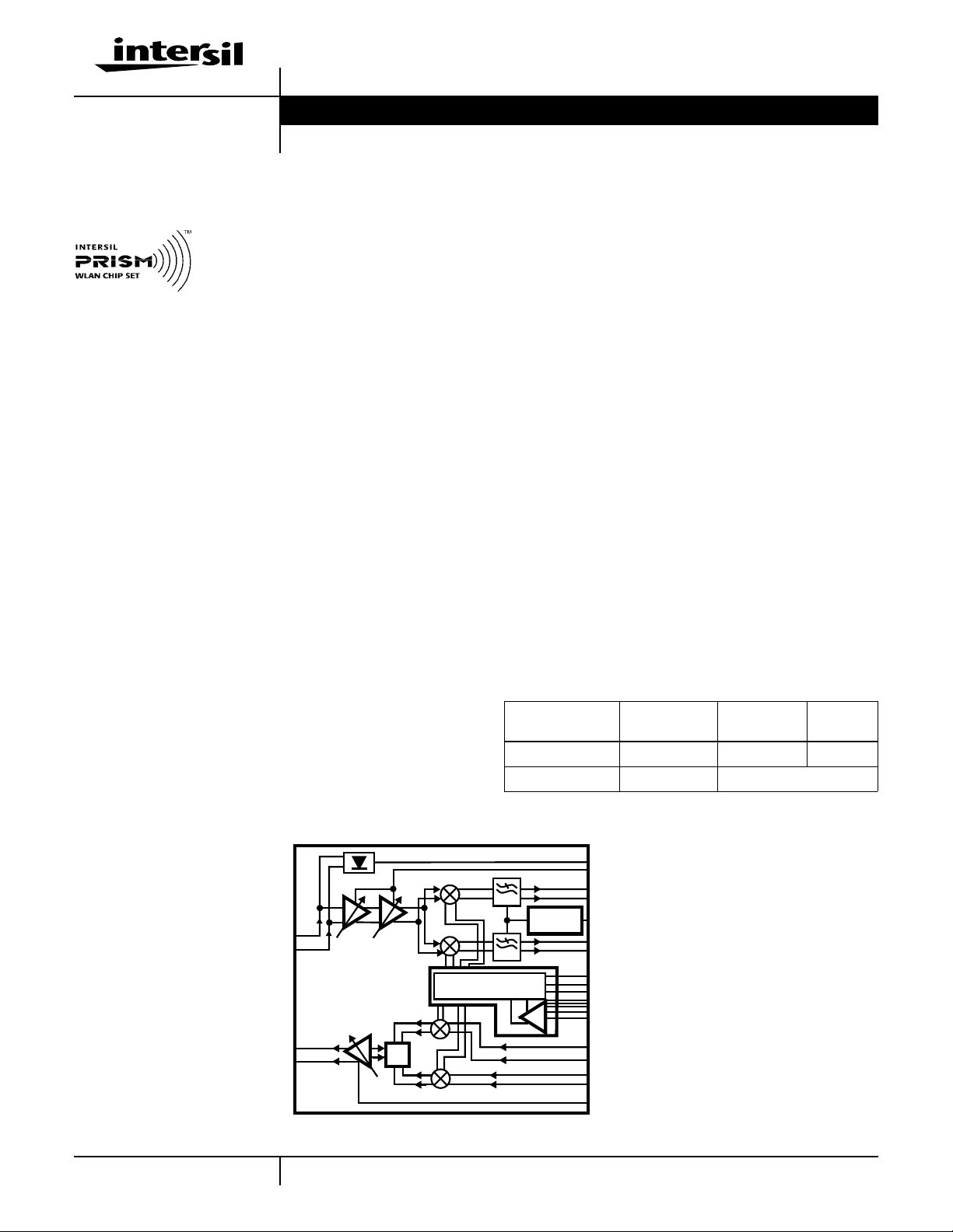
The HFA3783 is a highly integratedand
fully differential SiGe baseband
converter for half duplex wireless
applications. It features all the
necessary blocks for quadrature
modulation and demodulation of “I” and “Q” baseband
signals.
It has an integrated AGC receive IF amplifier with frequency
response to 600MHz. The AGC has 70dB of voltage gain
and better than 70dB of gain control range. The transmit
output also features gain control with 70dB of range.
The receive and transmit IF paths can share a common
differential matching network to reduce the filter component
count required for single IF half duplex transceivers.Apairof
2nd order antialiasing filters with an integrated DC offset
cancellation architecture is included in the receive chain for
baseband operation down to DC. In addition, an IF level
detector is included in the AGC chain for threshold
comparison. Up and down conversion are performed by
doubly balanced mixers for “I” and “Q” IF processing. These
converters are driven by a broadband quadrature LO
generator with frequency of operation phase locked by an
internal 3 wire interface synthesizer and PLL.
The device operates at low LO levels from an external VCO
with a PLL reference signal up to 50MHz. The HFA3783 is
housed in a thin 48 lead LQFP package well suited for
PCMCIA board applications.
File Number 4633.2
Features
• Integrates All IF Transmit and Receive Functions
• Broad Quadrature Frequency Range. . . . . .70 to 600MHz
• 600MHz AGC IF Strip with Level Detector. . . . . . . . .69dB
• DC Coupled Baseband Interfaces
• Integrates a Receiver DC Offset Calibration Loop
• Integrated 3 Wire Interface PLL For LO Applications
• Low LO Drive Level . . . . . . . . . . . . . . . . . . . . . . . -15dBm
• Fast Transmit-Receive Switching . . . . . . . . . . . . . . . .<1µs
• Power Management/Standby Mode
• Single Supply 2.7 to 3.3V Operation
Applications
• IEEE802.11 1 and 2Mbps Standard
• Systems Targeting IEEE 802.11 11Mbps Standard
• Wireless Local Area Networks
• PCMCIA Wireless Transceivers
• ISM Systems
• TDMA Packet Protocol Radios
Ordering Information
PART
NUMBER
HFA3783IN -40 to 85 48 Ld LQFP Q48.7x7A
HFA3783IN96 -40 to 85 Tape and Reel
TEMP. RANGE
(oC) PACKAGE PKG. NO.
Simplified Block Diagram
IF_IN
IF_OUT
1
IF DETECTOR OUT
RECEIVE AGC
I
OFFSET
CAL
Q
0o/90oPLL MODULE
∑
1-888-INTERSIL or 321-724-7143 | Intersil and Design is a trademark of Intersil Corporation. | Copyright © Intersil Corporation 2000
CAUTION: These devices are sensitive to electrostatic discharge; follow proper IC Handling Procedures.
PRISM is a registered trademark of Intersil Corporation. PRISM logo is a trademark of Intersil Corporation.
BASEBAND RXI
CAL ENABLE
BASEBAND RXQ
IF 2X LO / VCO IN
CHARGE PUMP OUT
3 WIRE INTERFACE
REF IN
BASEBAND TX I
BASEBAND TXQ
TRANSMIT IF AGC
Page 2
Pinout
HFA3783
CC
BB_V
DD
CP_D0
CP_V
GND
RXI+
373839404142434445464748
2423222120191817
GND
RXI-
36
35
34
33
32
31
30
29
28
27
26
25
LD
RXQ+
RXQTXI+
TXI-
1.2V_OUT
TXQ+
TXQGND
LO_V
CC
LO_IN+
LO_INGND
RX_V
CC
GND
IF_RX+
IR_RX-
GND
TX_VAGC
TX_V
CC
IF_TX+
IF_TX-
TX_V
CC
GND
GND
RX_VAGC
GND
1
2
3
4
5
6
7
8
9
10
11
12
13 14 15 16
REF_IN
REF_BYP
GND
GND
PE1
IF_DET
DD
GND
SYN_V
PE2
CLK
CAL_EN
GND
LE
DAT A
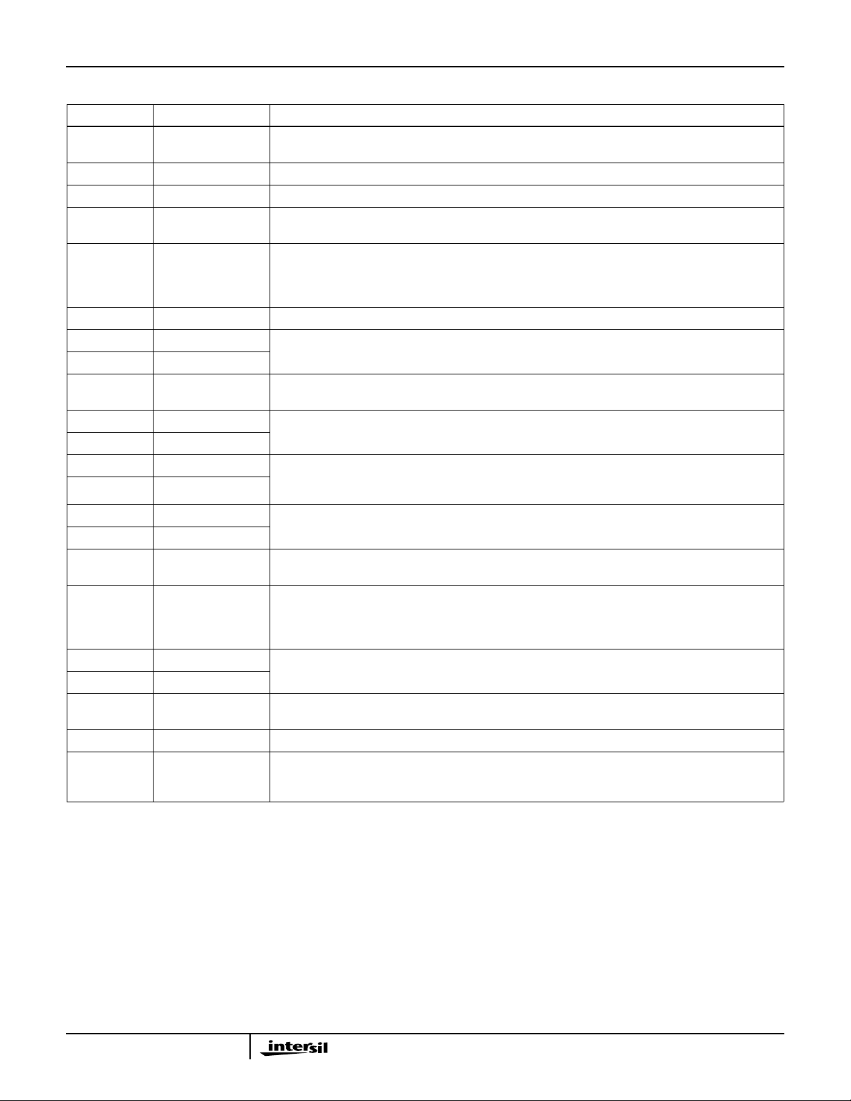
Pin Descriptions
PIN NUMBER NAME DESCRIPTION
1 RX_V
CC
3 IF_RX+ Receive AGC Differential Amplifier Non-Inverting IF Input. Requires a DC blocking capacitor.
4 IF_RX- Receive AGC Differential Amplifier Inverting IF Input. Requires a DC blocking capacitor. Pins 3 and 4 are
6 TX_VAGC Transmit AGC amplifier DC gain control input.
7 TX_V
CC
8 IF_TX+ Transmit AGC Differential Amplifier Positive Output. Open collector requiring DC bias from VCCthrough
9 IF_TX- Transmit AGC Differential Amplifier Negative Output. Open collector requiring DC bias from VCCthrough
10 TX_V
CC
13 REF_BYP PLL Reference Buffer Signal Negative Differential Input. Pin has active bias and can be used in
14 REF_IN PLLReferenceBufferSignal PositiveDifferential Input. Pin has active bias and can be used in conjunction
17 SYN_V
DD
18 CLK PLL Synthesizer Serial Interface Clock. CMOS input.
19 DATA PLL Synthesizer Serial Interface Data. CMOS input.
20 LE PLL Synthesizer Serial Interface Latch Enable Control. CMOS input.
Receive AGC Amplifier Power Supply. Requires high quality capacitor decoupling.
interchangeable and can be used single ended with the other being capacitively bypassed to ground.
Transmit AGC Amplifier Power Supply. Requires high quality capacitor decoupling.
an inductor.
an inductor.
Transmit AGC Amplifier Power Supply. Requires high quality capacitor decoupling.
conjunction with pin 14 either differential or single ended. CMOS inputs must be DC coupled. Small
sinusoidal inputs must be DC blocked with this pin bypassed to ground via a capacitor.
with pin 13 either differential or single ended. CMOS inputs must be DC coupled. Small sinusoidal inputs
must be DC blockedwith this pin used as an input for the reference signal. When used with single ended
CMOS inputs, pin 13 must be left floating. Pins 13 and 14 are interchangeable.
PLL Synthesizer Digital Power Supply. Requires high quality capacitor decoupling.
2
Page 3
HFA3783
Pin Descriptions (Continued)
PIN NUMBER NAME DESCRIPTION
21 CP_V
22 CP_D0 PLL Charge Pump Current Output.
24 LD PLL Lock Detect Output. Requires low capacitive loading not to exceed 5pF.
26 LO_IN- Local Oscillator Differential Buffer Negative Input. Requires AC coupling. For single ended applications
27 LO_IN+ Local Oscillator Differential Buffer Positive Input. Requires AC coupling. For single ended applications its
28 LO_V
30 TXQ- Baseband Quadrature Differential Inputs for IF Transmission. DC coupled requiring 1.3V common mode
31 TXQ+
32 1.2V_OUT Highly Regulated Band Gap 1.2V Buffered Output. Used in conjunction with ADCs and DACsfor voltage
33 TXI- Baseband In Phase Differential Inputs for IF Transmission. DC coupled requiring 1.3V common mode
34 TXI+
35 RXQ- Baseband Quadrature Differential Outputs FromIF Demodulation. DC coupled output with 1.2V common
36 RXQ+
37 RXI- Baseband In Phase Differential Outputs From IF Demodulation. DC coupled output with 1.2V common
38 RXI+
40 BB_V
42 CAL_EN CMOS Input forActivation Of Internal DC Offset Adjust Circuit for the Receive Baseband Outputs. A rising
43 PE2 Power Enable Control Pins: Please refer to the POWER ENABLE TRUTH TABLE in the Electrical
44 PE1
45 IF_DET IF Detector Current Output. A current source of 175µA typical is generated at this pin when the IF AGC
47 RX_VAGC Receive AGC amplifier DC gain control input.
2, 5, 11, 12, 15,
16, 23, 25, 29,
39, 41, 46, 48
DD
CC
CC
GND Grounds. Connect to a solid ground plane.
PLL Charge Pump Power Supply. Independent supply for the charge pump, not to exceed3.6V.Requires
high quality capacitor decoupling.
its complementary input, Pin 27, must be bypassed to ground via a capacitor.
complementary input, Pin 26, must be bypassed to ground via a capacitor. Pins 26 and 27 are
interchangeable.
NOTE: High second harmonic content LO waveforms may degrade I/Q phase accuracy.
Local Oscillator Buffer Amplifier Power Supply. Requires high quality capacitor decoupling.
bias voltages.
/temperature tracking. Requires high quality 0.1µF capacitor decoupling to ground.
bias voltages.
mode DC outputs. AC coupling pins 35, 36, 37 and 38 requires programmable register activation for DC
hold during TX to RX switching.
mode DC outputs.
Baseband Receive LPF Output and Offset Control Power Supply. Requires high quality capacitor
decoupling.
edge activates the calibration cycle, which completes within a programmable time and holds the
calibration while this pin is held high. In applications where the synthesizer is not used, this pin needs to
be grounded.
Specifications section.
receive differential or single ended signal at pins 3 and 4 is between 100 and 200mVPP.
3
Page 4

Application Circuit
HFA3783
SAW
SAWTEK
855653L1
V
CC
C
S
C
S
L
P
1000p
10µ
100p
2K
100p
L
P
1000p
0.01
1000p
0.01
100p
1000p
48
1
2
3
4
5
6
7
8
9
10
11
12
13
49.9
TX_VAGC
619
RX_VAGC
976
IF_DET
FROM MAC (CAL+ EN CTRL)
RX”I”
RX”Q”
0.01
2.87K
68p
47
46
44 43 42 41
45
LO
Σ
SYNTH
14
15
16
17
0.1
0/90
18
19
20
37383940
212223 24
0.1
36
35
34
33
32
31
30
29
28
27
26
25
0.022
56p
100p
100p
3.92K
0.22
2K
56
0.1
0.1
VT
3900pF
RF
VCO
PANASONIC
ENFV25F80
68p
536
536
124
TX”I”
124
124
TX”Q”
124
IDAC
7 BITS
IDAC
7 BITS
1-BIT
DET
ADC
6 BITS
ADC
6 BITS
DAC
6 BITS
1.2V REF IN
DAC
6 BITS
HFA3861
(SINUSOIDAL)
4
REF FREQ
FROM MAC (PLL CTRL)
VCO_V
10µ0.1
CC
Page 5

Test Diagram
FREQUENCY RESPONSE TEST SET UP
SWEEP
GEN.
50
V
CC
200p
50
ANALYZER
1000p
1000p
50
50
2
3
4
5
6
7
8
9
V
CC
10µ
IF_DET
RX_VAGC
.01
2.87K
PE1
PE2
HFA3783
CALIBRATION
RXI
CAL_EN
5KΩ INPUT
CALIBRATION
RXQ
.01
TX_VAGC
1000p
IF IN/OUT
TC4-1W
MATCH COMPONENTS FOR
TEST FIXTURE (374MHz)
AND TRANSFORMER
8p
8p
1000p
27n
100p
27n
100p
2K
.01
270p
1000p
1000p
100p
47
48
1
2
3
4
5
6
7
8
9
10
11
12
13
14
50
REF_IN
(SINUSOIDAL)
46
15
.1
270p
44 43 42 41
45
SYNTH
16
17
5KΩ INPUT
37383940
36
35
34
1.2V REF.
33
32
LO
∑
0/90
18
19
20
212223 24
VCC/2
LE
CLK
DAT A
31
30
29
28
27
26
25
.1
CP
.1
56p
100p
100p
BUFFER
.1
50
LO_IN (2X FREQ)
(LOW INPUT CAPACITANCE)
CALIBRATION
TXQ
1.2V_OUT
COMMON MODE VOLTAGE
CALIBRATION
TXI
COMMON MODE VOLTAGE
5
Page 6

HFA3783
Absolute Maximum Ratings Thermal Information
Voltage on Any Other Pin. . . . . . . . . . . . . . . . . . . -0.3 to VCC+0.3V
VCC to VCC Decouple or Gnd to Gnd . . . . . . . . . . . . . -0.3 to +0.3V
Any Pin to Gnd. . . . . . . . . . . . . . . . . . . . . . . . . . . . . . . . . . . . . . 4.0V
Operating Conditions
Operating Temperature Range . . . . . . . . . . . . . . . . . . -40 to +85oC
Supply Voltage Range. . . . . . . . . . . . . . . . . . . . . . . . . . . . . 2.7-3.3V
CAUTION: Stresses above those listed in “Absolute Maximum Ratings” may cause permanent damage to the device. This is a stress only rating and operation of the
device at these or any other conditions above those indicated in the operational sections of this specification is not implied.
NOTE:
1. θJAis measured with the component mounted on an evaluation PC board in free air.
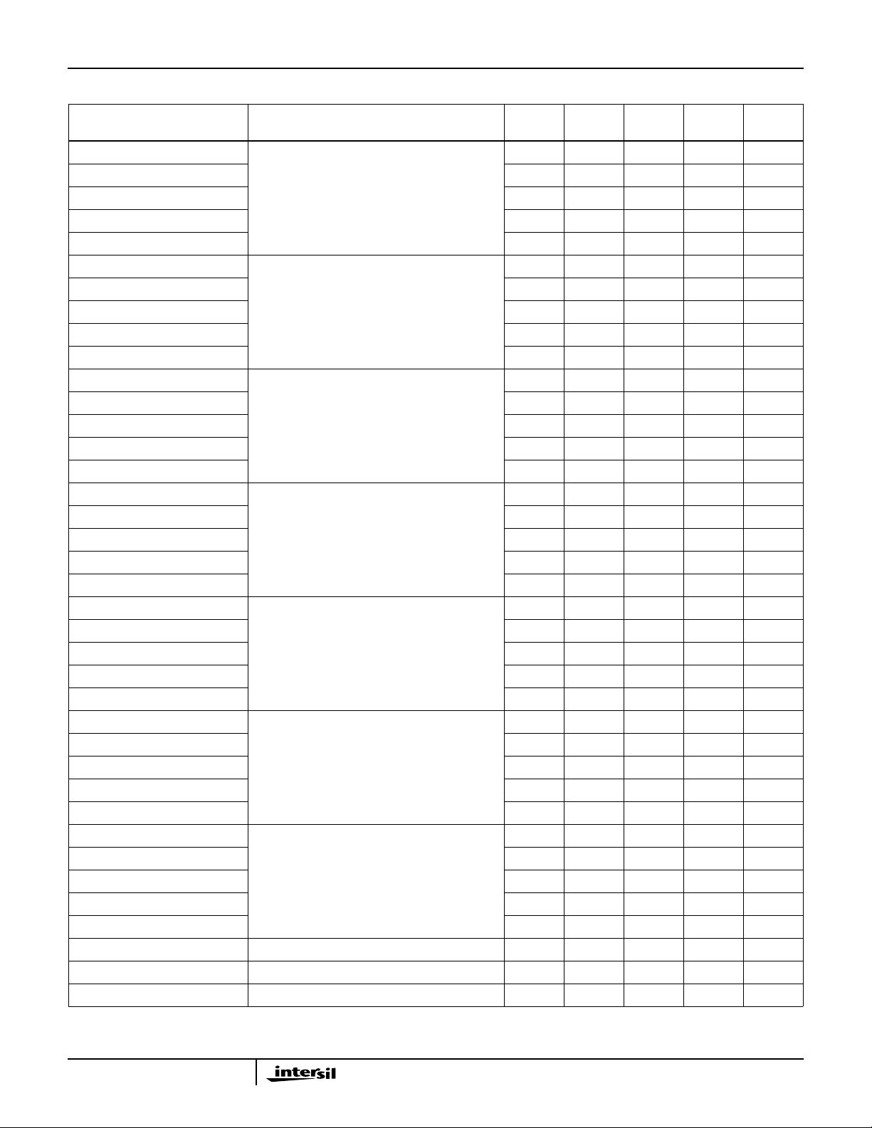
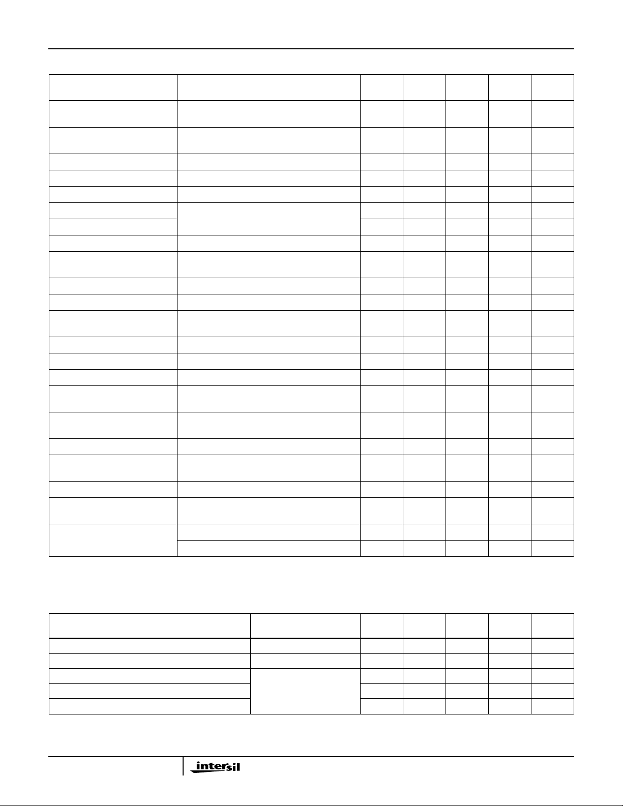
DC Electrical Specifications
PARAMETER
Supply Voltage Full 2.7 - 3.3 V
Receive Total Supply Current 25 - 36 40 mA
Transmit Total Supply Current 25 - 32 40 mA
Voltage Reference Output at ±1mA, 0.1µF Load Full 1.14 1.2 1.26 V
NOTE: TX/RX Power Down Supply Current (PLL Serial Interf. Active) (Note 2) Full - - 100 µA
TX/RX/Power Down Speed (Note 3) Full - - 10 µs
RX/TX, TX/RX Switching Speed (Note 3) Full - - 1 µs
CMOS Low Level Input Voltage Full -0.3 - 0.3*V
CMOS High Level Input Voltage (VDD = 3.6V) Full 0.7*V
CMOS Threshold Voltage Full - 0.5*V
CMOS High or Low Level Input Current Full -3.0 - +3.0 µA
NOTE:
2. Standby current is measured after a long elapsed time (20 seconds).
3. TX/RX/TX switching speed and power Down/Up speed are dependent on external components.
Thermal Resistance (Typical, Note 1) θJA (oC/W) θJC (oC/W)
LQFP Package. . . . . . . . . . . . . . . . . . . 70 N/A
Maximum Junction Temperature (Plastic Package) . . . . . . . . . . 150
Maximum Storage Temperature Range. . . . . . . . . . . . . . .-65 to 150
Maximum Lead Temperature (Soldering 10s) . . . . . . . . . . . . . . .300
Moisture Sensitivity Level (Intersil Tech. Brief TB363). . . . . .168 Hrs
TEMP.
(oC) MIN TYP MAX UNITS
V
DD
DD
- 3.6 V
DD
-V
Receive Cascaded AC Electrical Specification IF = 375MHz, LO = 748MHz, V
PARAMETER TEST CONDITIONS
IF Frequency Range Test Diagram Full 70 - 600 MHz
2XLO Frequency Range Test Diagram Full 140 - 1200 MHz
Maximum Power Gain VAGC = 0V 25 56 61 dB
Voltage Gain Nominal High Gain. Differential 250Ω in, 5kΩ
Power Gain Full - 56 - dB
Cascaded Noise Figure Full - - 8 dB
Output IP3 Full +2.2 - - dBm
Output P1dB Full -14.1 - - dBm
output differential load.
AGC Control voltage set to 69dB of voltage gain
= 2.7V, Unless Otherwise Specified
CC
TEMP.
(oC) MIN TYP MAX UNITS
Full - 69 - dB
6
Page 7
HFA3783
Receive Cascaded AC Electrical Specification IF = 375MHz, LO = 748MHz, V
PARAMETER TEST CONDITIONS
Voltage Gain AGC Control Voltage set to 10dB attenuation.
Power Gain Full - 46 - dB
Cascaded Noise Figure Full - - 11 dB
Output IP3 Full +1.5 - - dBm
Output P1dB Full -14.3 - - dBm
Voltage Gain AGC Control Voltage set to 20dB attenuation.
Power Gain Full - 36 - dB
Cascaded Noise Figure Full - 14.1 - dB
Output IP3 Full +1.0 - - dBm
Output P1dB Full -14.4 - - dBm
Voltage Gain AGC Control Voltage set to 30dB attenuation.
Power Gain Full - 26 - dB
Cascaded Noise Figure Full - 19.9 - dB
Output IP3 Full +0.3 - - dBm
Output P1dB Full -14.6 - - dBm
Voltage Gain AGC Control Voltage set to 40dB attenuation.
Power Gain Full - 16 - dB
Cascaded Noise Figure Full - 27 - dB
Output IP3 Full -1.4 .74 2.8 dBm
Output P1dB Full -15.0 - - dBm
Voltage Gain AGC Control Voltage set to 50dB attenuation.
Power Gain Full - 6 - dB
Cascaded Noise Figure Full - 35.1 - dB
Output IP3 0-85 -2.0 - - dBm
Output P1dB 0-85 -15.5 - - dBm
Voltage Gain AGC Control Voltage set to 60dB attenuation.
Power Gain Full - -4 - dB
Cascaded Noise Figure Full - 43.9 - dB
Output IP3 0-85 -3.3 - - dBm
Output P1dB 0-85 -16.1 - - dBm
Voltage Gain AGC Control Voltage set to 72dB attenuation.
Power Gain Full - -16 - dB
Cascaded Noise Figure Full - 60.0 - dB
Output IP3 0-85 -6.7 - - dBm
Output P1dB 0-85 -18.2 - - dBm
Minimum Power Gain VAGC = 2.25V 25 - - -17 dB
AGC Gain Control Voltage Full 0.2 - 2.25 V
AGC Gain Control Sensitivity Over Supply Range Full - 61.6 - dB/V
Differential 250Ω input, differential 5kΩ output
load.
Differential 250Ω input, differential 5kΩ output
load.
Differential 250Ω input, differential 5kΩ output
load.
Differential 250Ω input, differential 5kΩ output
load.
Differential 250Ω input, differential 5kΩ output
load.
Differential 250Ω input, differential 5kΩ output
load.
Differential 250Ω input, differential 5kΩ output
load.
= 2.7V, Unless Otherwise Specified (Continued)
CC
TEMP.
(oC) MIN TYP MAX UNITS
Full - 59 - dB
Full - 49 - dB
Full - 39 - dB
Full - 29 - dB
Full - 19 - dB
Full - 9 - dB
Full - -3 - dB
7
Page 8
HFA3783
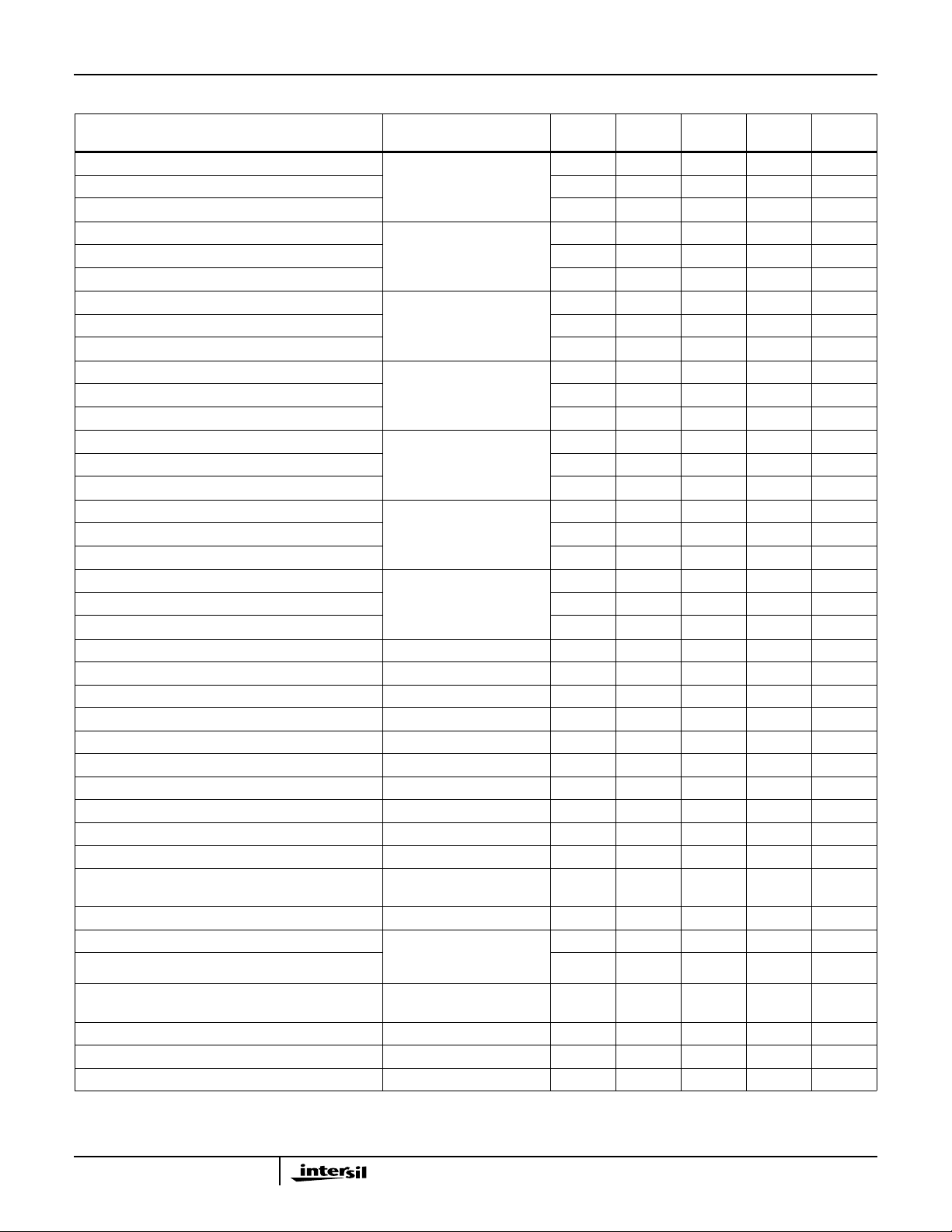
Receive Cascaded AC Electrical Specification IF = 375MHz, LO = 748MHz, V
PARAMETER TEST CONDITIONS
AGC Gain Control Input
Impedance
Gain Switching Speed to ±1dB
Settling
Insertion Phase vs AGC Full AGC Range 25 -2 ±0.3 +2 deg/dB
IF Detector Response Time 10pF, 2.9K External Load Full - 0.15 0.25 µs
IF Detector Input Voltage 0.5V, 175µA Into 2.87K Out Full 100 150 200 mV
LO Internal Input Resistance Single End. 748MHz 25 950 - 1.1K Ω
LO Internal Input Capacitance 25 - 0.96 - pF
LO Drive Level External 50Ω Match Network (single resistor) Full -15 -10 0 dBm
Upper Baseband 3dB Bandwidth
(2nd Order)
Lower Baseband 3dB Bandwidth DC Coupled Load Full DC - - I and Q 3dB BW Matching Full -2 - +2 %
Cascaded Receive I or Q
Baseband THD
Cascaded Receive I/Q Crosstalk 25 - - -40 dB
I/Q Amplitude Balance 100kHz CW Full -1 - +1 dB
I/Q Phase Balance 100kHz CW Full -2 - +2 deg
Cascaded I or Q Baseband
Differential Offset Voltage
Cascaded I or Q Common Mode
Voltage at Baseband
Offset Calibration Time Ref = 44MHz, Offset Counter C = 25 Full - 25 - µs
Offset Counter Divide Ratio
(C Counter)
CAL_EN Minimum Pulse Width High to Low to High Transition Time Full 0 - - nS
Baseband Output Resistance
Loading
Baseband Output Capacitance
Loading
NOTE:
4. A positive frequency offset from the carrier produces I leading Q by 90 degrees.
Full AGC Scale Full - 0.4 1 µs
1MHz, 1VPP Diff. for First 50dB of Attenuation
Range
AfterCalibration Cycle. Measured witha setting of
26dB of power gain
Input Ref Clock is Divided by C*2 for SAR Offset
Correction
Differential. 1/2 value for ground reference loads Full - 5 - kΩ
Single End, Each Full - - 10 pF
Differential Full - - 10 pF
= 2.7V, Unless Otherwise Specified (Continued)
CC
TEMP.
(oC) MIN TYP MAX UNITS
Full 20 23 - kΩ
Full 6.7 7.4 8.5 MHz
25 - - 1 %
Full - - 10 mV
Full 1.08 1.17 1.32 V
Full 1 - 127 -
PP
T ransmit Cascaded AC Electrical Specifications LO = 748MHz, V
PARAMETER TEST CONDITIONS
IF Frequency Range Test Diagram Full 70 - 600 MHz
2 X LO Frequency Range Test Diagram Full 140 - 1200 MHz
Output Power at 250Ω Differential Load AGC Voltage Set to -10dBm
Output Noise Floor Full - -141 - dBm/Hz
P1dB/Output Power Ratio Full 10 - - dB
Output Power for 0.35V
Sine I and Q
Inputs
= 2.7V, VCM = 1.24V Unless Otherwise Specified
CC
TEMP.
(oC) MIN TYP MAX UNITS
Full - -10 - dBm
PP
8
Page 9
HFA3783
T ransmit Cascaded AC Electrical Specifications LO = 748MHz, V
= 2.7V, VCM = 1.24V Unless Otherwise Specified (Continued)
CC
TEMP.
PARAMETER TEST CONDITIONS
Output Power at 250Ω Differential Load AGC Voltage Set to 10dB
Output Noise Floor Full - -149 - dBm/Hz
P1dB/Output Power Ratio Full 10 - - dB
Attenuation.
0.35VPP Sine I and Q
Inputs
Output Power at 250Ω Differential Load AGC Voltage Set to 20dB
Output Noise Floor Full - -157 - dBm/Hz
P1dB/Output Power Ratio Full 10 - - dB
Attenuation.
0.35V
Sine I and Q
PP
Inputs
Output Power at 250Ω Differential Load AGC Voltage Set to 30dB
Output Noise Floor Full - -161 - dBm/Hz
P1dB/Output Power Ratio Full 10 - - dB
Attenuation.
0.35V
Sine I and Q
PP
Inputs
Output Power at 250Ω Differential Load AGC Voltage Set to 40dB
Output Noise Floor Full - -162 - dBm/Hz
P1dB/Output Power Ratio Full 10 - - dB
Attenuation.
0.35V
Sine I and Q
PP
Inputs
Output Power at 250Ω Differential Load AGC Voltage Set to 50dB
Output Noise Floor Full - -163 - dBm/Hz
P1dB/Output Power Ratio Full 10 - - dB
Attenuation.
0.35V
Sine I and Q
PP
Inputs
Output Power at 250Ω Differential Load AGC Voltage Set to 60dB
Output Noise Floor Full - -164 - dBm/Hz
P1dB/Output Power Ratio Full 10 - - dB
Attenuation.
0.35V
Sine I and Q
PP
Inputs
Output Power at 250Ω Differential Load AGC Voltage Set to 70dB
Output Noise Floor Full - -164 - dBm/Hz
P1dB/Output Power Ratio Full 10 - - dB
Attenuation.
0.35V
Sine I and Q
PP
Inputs
(oC) MIN TYP MAX UNITS
Full - -20 - dBm
Full - -30 - dBm
Full - -40 - dBm
Full - -50 - dBm
Full - -60 - dBm
Full - -70 - dBm
Full - -80 - dBm
AGC Gain Control Voltage Full 0.1 - 2.25 V
AGC Gain Control Sensitivity Supply Range 25 - 35.4 - dB/V
AGC Control Input Impedance Full 20 21 - kΩ
Gain Switching Speed to ±1% Settling Full Scale 25 - 0.8 4 µs
Insertion Phase vs AGC 50dB Range from Max Full - - 4.0 deg
I/Q Baseband Bandwidth Application Circuit Full 0 13 - MHz
Cascaded Baseband to IF TX THD 1MHz, 0.5V
PP
25 - - 0.5 %
Amplitude Balance DC Inputs 25 -0.5 - +0.5 dB
Phase Balance DC Inputs 25 -2 - +2 deg
Carrier Suppression Full AGC Range 25 - -43 -30 dBc
SSB Sideband Suppression (Note 5) 100kHz Inputs, Full AGC
25 - -43 -32 dBc
Range
Optimum IF Output Differential Impedance Shared with RX 25 - 250 - Ω
LO Internal Input Resistance Single End
LO Internal Input Capacitance 25 - 0.96 - pF
Across F. Range
Same as RX Section
LO Drive Level External 50Ω Match
25 950 - 1.1K Ω
Full -15 -10 0 dBm
Network (single resistor)
Baseband Differential Input Impedance Full 100 150 - kΩ
Optimum Baseband Differential Input Voltage Shaped Pulses Full - 0.5 - V
PP
Common Mode Baseband Input Voltage Range All TX Inputs Full 1.2 1.30 1.40 V
NOTE:
5. I leading Q produces a+jw CCW rotation and a positive frequency offset from the carrier.
9
Page 10
HFA3783
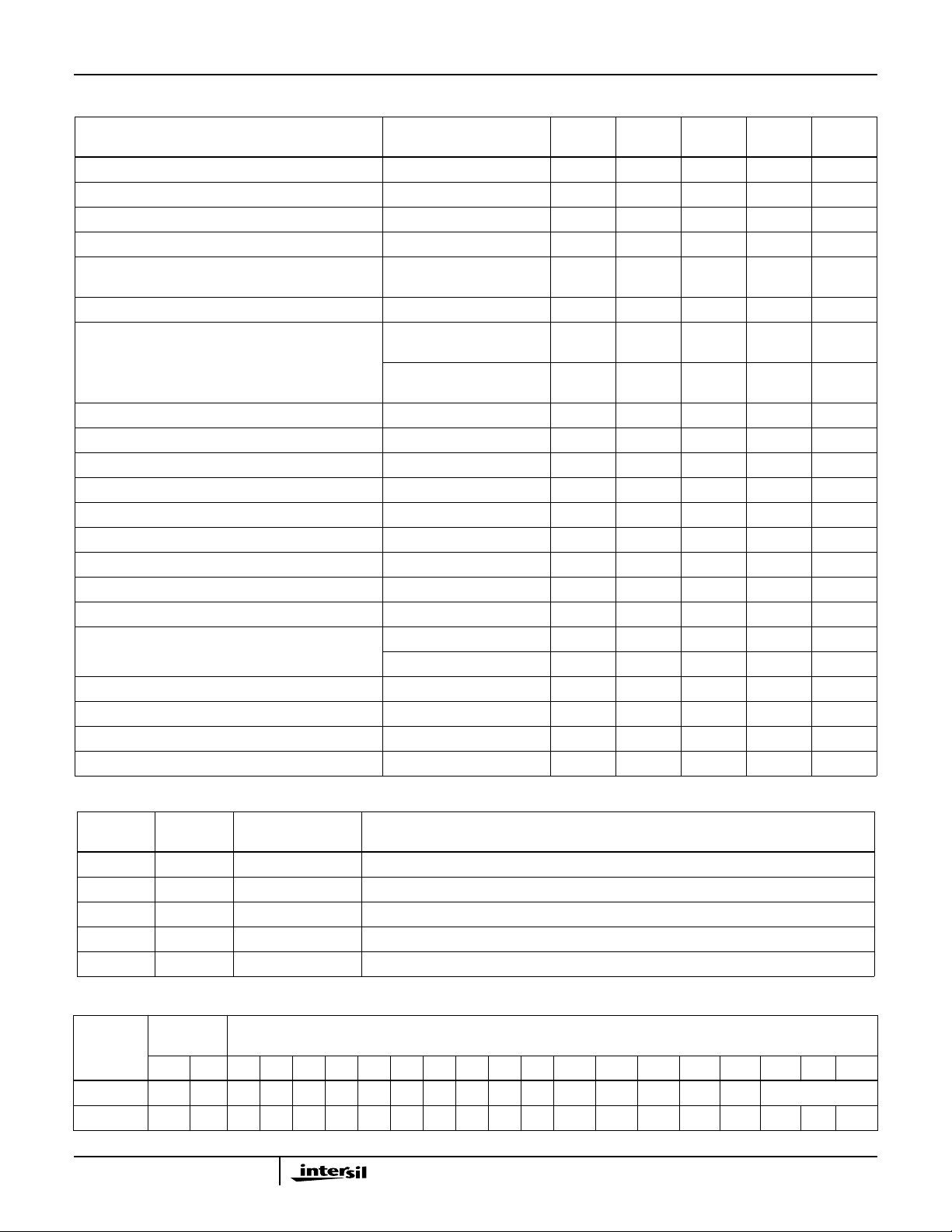
Phase Lock Loop Electrical Specifications
TEMP.
PARAMETER TEST CONDITIONS
Operating 2X LO Frequency Test Diagram Full 140 - 1200 MHz
Reference Oscillator Frequency Test Diagram Full - - 50 MHz
Selectable Prescaler Ratios (2 Settings) Full 16/17 N/A 32/33 Swallow Counter Divide Ratio (A Counter) Full 0 - 127 Programmable Counter Divide Ratio
(B Counter)
Reference Counter Divide Ratio (R Counter) Full 3 - 32767 Reference Oscillator Sensitivity Single or Differential Sine
Inputs
CMOS Single or
Complementary
Reference Oscillator Duty Cycle CMOS Inputs Full 40 - 60 %
Charge Pump Sink/Source Current/Tolerance 250µA Selection +/- 25% Full 0.18 0.25 0.32 mA
Charge Pump Sink/Source Current/Tolerance 500µA Selection +/- 25% Full 0.375 0.5 0.625 mA
Charge Pump Sink/Source Current/Tolerance 750µA Selection +/- 25% Full 0.56 0.75 0.94 mA
Charge Pump Sink/Source Current/Tolerance 1mA Selection +/- 25% Full 0.75 1.0 1.25 mA
Charge Pump Sink/Source Mismatch Full - - 15 %
Charge Pump Output Compliance Full 0.5 - CPVDD-0.5 V
Charge Pump High Z leakage High Z state Full -10 ±0.1 10 µA
Charge Pump Supply Voltage Full 2.7 - 3.6 V
Serial Interface Clock Width High Level Full 20 - - ns
Low level Full 20 - - ns
Serial Interface Data/Clk Set-Up Time Full 20 - - ns
Serial Interface Data/Clk Hold Time Full 10 - - ns
Serial Interface Clk/LE Set-Up Time Full 20 - - ns
Serial Interface LE Pulse Width Full 20 - - ns
(oC) MIN TYP MAX UNITS
Full 3 - 2047 -
Full 0.5 - - V
Full - CMOS - -
PP
POWER ENABLE TRUTH TABLE
PLL_PE
PE1 PE2
0 0 1 Power Down State, PLL Registers in Save Mode, Inactive PLL, Active Serial Interface
1 1 1 Receive State, Active PLL
1 0 1 Transmit State, Active PLL
0 1 1 Inactive Transmit and Receive States, Active PLL, Active Serial Interface
X X 0 Inactive PLL, Disabled PLL Registers, Active Serial Interface
(SERIAL BUS) STATUS
PLL Synthesizer and DC Offset Clock Programming Table
REGISTER
SERIAL
BITS
R Counter 0 0 R(0) R(1) R(2) R(3) R(4) R(5) R(6) R(7) R(8) R(9) R(10) R(11) R(12) R(13) R(14) X (Don’t Care)
A/B Counter 0 1 A(0) A(1) A(2) A(3) A(4) A(5) A(6) B(0) B(1) B(2) B(3) B(4) B(5) B(6) B(7) B(8) B(9) B(10)
DEFINITION
LSB 1 2 345678910111213 14 1516171819MSB
10
Page 11

HFA3783
PLL Synthesizer and DC Offset Clock Programming Table (Continued)
REGISTER
SERIAL
BITS
Operational
Mode
Offset
Calibration
NOTES:
6. The Serial data is clocked on the Rising Edge of the serial clock, MSB first. The serial Interface is active when LE is LOW. The serial Data is
latched into defined registers on the rising edge of LE.
7. The M register or Operational Mode needs to be loaded first. Registers R, A/B and Offset Calibration follow M loading in any sequence.
Reference Frequency Counter/Divider
R(0-14) Least significant bit R(0) to most significant bit R(14) of the divide by R counter. The Reference signal frequency is divided down
LO Frequency Counters/Dividers
A(0-6) Least significant bit A(0) to most significant bit A(6) of a 7-bit Swallow counter and LSB B(0) to MSB B(10) of the 11 bits divider.
B(0-10)
DEFINITION
LSB 1 2 345678910111213 14 1516171819MSB
1 0 M(0) 0 M(2) M(3) M(4) M(5) M(6) M(7) M(8) 0 0 0 0 M(13) M(14) M(15) X X
1 1 C(0) C(1) C(2) C(3) C(4) C(5) C(6) 0 0 0 0 C(11) X (Don’t Care)
BIT DESCRIPTION
by this counter and is compared with a divided LO by a phase detector.
BIT DESCRIPTION
The LO frequency is divided down by [P*B+A], where P is the prescaler divider set by bit M(2). This divided signal frequency is
compared by a phase detector with the divided Reference signal.
Operational Modes
BIT DESCRIPTION
M(0) (PLL_PE), Phase Lock Loop Power Enable. 1 = Enable, 0 = Power Down. Serial port always on.
M(2) Prescaler Select. 0 = 16/17, 1 = 32/33
M(3)
M(4)
M(5)
M(6)
M(7)
M(8)
M(13)
M(14)
M(15)
Charge Pump Current Setting. M(4) M(3) OUTPUT SINK/SOURCE
0 0 0.25mA
0 1 0.50mA
1 0 0.75mA
1 1 1.00mA
Charge Pump Sign. M(6) M(5)
0 0 Source Current if LO/ [P*B+A] < Ref/R
0 1 Source Current if LO/ [P*B+A] > Ref/R
LD Pin Multiplex Operation. M(13) M(8) M(7) OUTPUT AT PIN LD
0 0 X Lock Detect Operation
0 1 X Short to GND
1 0 X Serial Register Read Back
1 1 0 Ref. Divided by R Waveform
1 1 1 LO Divided by [P*B+A]
Charge Pump Operation/Test. M(15) M(14) OPERATION/TEST
0 0 Normal Operation
0 1 Charge Pump Constant Current Source
1 0 Charge Pump Constant Current Sink
1 1 High Impedance State
Waveform
11
Page 12

HFA3783
DC Offset Calibration Counter
BIT DESCRIPTION
C(0-6) Least Significant bit C(0) to Most significant bit C(6) of the offset calibration counter/divider. The calibration clock frequency and
calibration time is defined by the Reference signal frequency divided down by this counter as follows:
2∗C
∗
CAL TIME = 22
C(11) Set output bias level for AC coupling applications and TX/RX switching improvement in performance.
----------------------------------- -
REFIN (MHz)
CLK
DAT A
LE
MSB
BIT 20
DAT/CLK
SET UP
CLK WIDTH
HIGH
CLK WIDTH
LOW
BIT 2
DAT/CLK
HOLD
FIGURE 1. PLL SYNTHESIZER SERIAL INTERFACE TIMING DIAGRAM
CLK/LE
SET UP
LSB
BIT 1
LE
P. WIDTH
12
Page 13

S Parameter Tables
HFA3783
RX DIFFERENTIAL INPUT, LINEAR MODE
FREQ (MHz) MAG ANGLE
70 0.886 -2.6
140 0.886 -4.7
200 0.886 -6.6
280 0.885 -9.4
380 0.885 -12.8
500 0.883 -16.9
600 0.883 -20.1
RX DIFFERENTIAL INPUT, TX MODE
FREQ (MHz) MAG ANGLE
70 0.877 -4.4
140 0.873 -7.4
200 0.870 -10.5
280 0.866 -14.5
380 0.862 -19.6
500 0.857 -25.7
600 0.853 -30.5
RX DIFFERENTIAL INPUT, SATURATED
FREQ (MHz) MAG ANGLE
70 0.883 -2.5
140 0.881 -5.7
200 0.878 -8.4
280 0.875 -11.9
380 0.869 -16.2
500 0.859 -21.3
600 0.850 -25.4
TX DIFFERENTIAL OUTPUT
FREQ (MHz) MAG ANGLE
70 1 -1.1
140 1 -2.0
200 0.999 -2.8
280 0.999 -3.9
380 0.999 -5.4
500 0.999 -7.1
600 0.997 -8.3
TX DIFF OUT AT RX-MODE
FREQ (MHz) MAG ANGLE
70 1 -1.0
140 1 -1.9
200 1 -2.8
280 1 -3.9
380 1 -5.2
500 0.999 -6.8
600 0.999 -8.0
LO INPUT SINGLE END
FREQ (MHz) MAG ANGLE
140 0.923 -5.1
400 0.920 -13.4
560 0.917 -19.0
760 0.911 -25.9
1000 0.900 -34.8
1200 0.890 -42.3
REF IN SINGLE END
RESISTOR /CAPACITANCE
FREQ (MHz)
10 5.8K 0.840p
30 5.7K 0.850p
50 5.7K 0.860p
RX SINGLE END IN LINEAR MODE
FREQ (MHz) MAG ANGLE
70 0.873 -4.0
140 0.872 -7.1
200 0.870 -10.1
280 0.869 -14.2
380 0.870 -19.3
500 0.872 -25.6
600 0.872 -30.8
PARALLEL
13
Page 14

HFA3783
Overall Device Description
The HFA3783 is a highly integrated baseband converter for
half duplex wireless data applications. It features all the
necessary blocks for baseband modulation and
demodulation of “I” and “Q” quadrature multiplexing signals
including an on chip three wire interface PLL stage used with
an external VCO for Local Oscillator applications. Device RF
properties have been optimized through the thoughtful
consideration of layout, device pinout, and a completely
differential design. These RF properties include immunity
from common mode signals such as noise and crosstalk,
optimized dynamic range for low power requirements and
reduced relevant parasitics and settling times. The single
power supply requirements from 2.7V
the HFA3783 a good choice for portable transceiver designs.
Receive Chain
The HFA3783 has two cascaded very low distortion
integrated AGC IF amplifiers with frequency response from
70 to 600MHz. These differential amplifiers exhibit better
than 70dB of both voltage gain and AGC range. Noise figure,
output compression and intercept point variations with the
AGC range have been tailored to achieve cascaded
performances as presented in the AC Electrical
Specifications. To increase the receiver’s overall AGC
dynamic range and conserve compression specifications, a
Peak Detector has been added in parallel with the AGC’s
input. The Peak Detector is used to control an external step
attenuator or the RF gain of the front end LNA stage.
Following the AGC stages, an AC coupled down conversion
pair of quadrature doubly balanced mixers are used for “I”
and “Q” baseband IF processing. These differential
converters are driven by an internal differential quadrature
generator with broadband response and excellent
quadrature properties. For broadband operation, the Local
Oscillator frequency input is twice the desired frequency of
demodulation. Duty cycle and signal purity requirements for
the 2XLO input using this type of quadrature architecture are
less restrictive for the HFA3783. Ground reference or
differential input signals from -15dBm to 0dBm and
frequencies up to 1200MHz (2XLO) can be used.
The output of the “I” and “Q” mixers are DC coupled to a pair
of multistage differential 2nd pole antialiasing baseband
filters with DC offset correction. The DC offset correction is
enabled with an external control pin allowing for correction to
occur during transmit, receive or power down modes. The
baseband filter’s cut off frequency of 7.7MHz is optimized for
11M chips/s spread spectrum applications. The baseband
outputs are differential, with common mode DC voltage
outputs tracking an internal band gap voltage reference. The
Band Gap reference is also available to the user by an
external pin. The “I” and “Q” baseband voltages can swing
up to 1Vpp differential, following the AC Electrical
Specifications across the AGC range. Figure 16 illustrates
the cascaded gain characteristics versus AGC voltage
control for the HFA3783 receive section.
to 3.3VDC makes
DC
Transmit Chain
The HFA3783 modulator section has a frequency response
of 70 to 600MHz. It consists of differential “I” and “Q”
baseband inputs requiringpre-shaped analog data levels up
to 500mVpp. A common mode voltage of around 1.3V is
required for proper operation of the four differential input
pins. There are no internal pre-shaping filters in the
modulator section. Following the differential input stages, a
DC coupled up conversion pair of quadrature doubly
balanced mixers are used for “I” and “Q” baseband IF
processing. These differential mixers are driven by the same
internal LO quadrature generator used in the receive
section. Their phase and gain characteristics, including I/Q
matching, are well suitable for accurate data transmission.
The final stage is an AGC amplifier with 70dB of dynamic
range. Please refer to Figure 35.
Detailed Description
Receive AGC/ Peak Detector
The receive AGC amplifier section consists of 4 stages and
each stage is built out of four parallel, distributed
gain/degeneration differential pairs. In half duplex packet
transmission linear systems, the receive AGC control’s
thermal and supply voltage variations over the packet
duration are more important than gain control linearity.
Therefore, the chosen architecture addresses very
constricted temperature,voltage and process variations. The
control is based on a band gap voltage reference “gm”
distribution scheme. In addition, the design provides fast
AGC settling times as well as fast turn on/off characteristics
for packetized information. The four stage AGC amplifier has
a typical maximum voltage gain of 44dB and exhibits better
than 70dB of dynamic range, providing an attenuation in
excess of 26dB at minimum gain. The design can be used
differential or single ended, exhibiting the same gain
characteristics: however, consideration is necessary due to
common mode spurious signals. One of the main features of
this front end is the high impedance and small variation of S
parameters when the HFA3783is switched between transmit
and receive modes. This feature permits the use of a
combination match network and the use of a single SAW
filter for both halves of the duplex operation. S parameters
for the differential and single ended applications are
available in the S Parameter Tables of this document. The
matching network arrangements will be discussed later in IF
Interface section.
A PeakDetector is placed in parallel with the input of the first
stage of the AGC amplifier. It consists of a high frequency
differential full wave rectifier and a voltage to current
converter. The Peak Detector has limited range and is used
to trip a comparator in an external baseband processor
when the voltage swing at the input of the AGC amplifier is
about 150mVpp. Once the external comparator is tripped,its
logic output level steps the LNA’s gain down keeping the RF
14
Page 15

HFA3783
and IF mixers out of compression. An external resistor and
capacitor set both the desired threshold voltage and time
constant. Figures 29 and 30 illustrate the typical current
output of the Peak Detector for input voltage levels between
100 and 200mVpp.
Quadrature Demodulator
The output of the AGC amplifier is AC coupled to two doubly
balanced quadrature differential mixers, for “I” and “Q”
demodulation. With full balanced differential architecture,
these mixers are driven by an accurate internal Local
Oscillator (LO) chain as described later. The voltage gain for
both mixers is well matched with a typical value of 8V/V.
Low Pass Filter and DC Offset Correction
To cover baseband signals from DC to 7.7MHz, the outputs
of the baseband down converter mixers are DC coupled to
the Low Pass Filter stages. For true DC response, the
combination of all DC offsets (mixer,LPF and buffers) needs
to be calibrated for accurate baseband processing. This
calibration can be performed at any time during the receive,
transmit or power down modes. Figure 2 depicts the
baseband low pass receive filter implementation and Figure
3 shows the calibration internal timing diagram of the
HFA3783. Referring to channel “I” for example, calibration
begins with the auto balanced comparator measuring the
differential offset between the RXI+ and RXI- outputs. The
comparator’s output is fed to a decision circuit which
changes the condition of a Successive Approximation
Register (SAR) state control. The SAR controls 8 bits of a
current output Digital to Analog Converter (IDAC) which is
divided by weight into a LPF section (2 pole) and a buffer
amplifier. The currents are searched and set to bring the
offset to a minimum. The LPF has a fixed gain of 2.5V/V and
the buffer adds a 1.25V/V final gain to the receive chain.
Referring to Figure 2, clocking to the SAR is provided by a
programmable division of the REF_IN signal. (Used for the
PLL as the stable reference.) The frequency of the reference
signal is divided down by the register setting of the offset
calibration counter. (Details for setting this counter can be
found in the Programming the PLL Synthesizer and DC
Offset Clock section.)
The output of the calibration counter is again divided by 2
and the period used to generate the time slots of a state
sequence. The calibration cycle is initialized by a rising edge
on the HFA3783 CAL_EN pin. The state sequence slots 1 to
7 are used to settle all circuits in case the device is in the
power down mode, slots 8 to 10 are used to calibrate the
offset comparators (auto balancing) and slots 13 to 21
perform the search with an initial value of approximately + or
- 400mV differential DC level. The comparator reads the
direction and level of the offset and sets the next level and
polarity at + or -400/2 mV. The process continues until slot
21 in a divide by 2 polarity and minimum offset search. The
contents of the SAR are kept in slot 22 which holds the IDAC
in storage mode until a new positive edge is provided to the
CAL_EN pin. In receivemode, the AGC amplifiers are turned
off during the calibration cycle. A typical calibration time from
10 to 25µS is suggested for optimum accuracy.
The baseband outputs of the LPF buffer amplifier drive
differential loads of 5KΩ with a common mode voltage of
typically 1.17V.
An extra feature of the LPF allows for AC coupling of the
baseband differentialoutputs. To avoiddischarging of the AC
coupling capacitors between transmit and receive states a
common mode voltage can be applied to all outputs. An
onboard programmable bit control establishes the
application with 4 internal resistors and switches.
LO Quadrature Generator
The In Phase and Quadrature Local oscillator signals are
generated by a divide by two circuit that drives both the up
and down conversion mixers. With a fully balanced
approach, the phase relationship between the two
quadrature signals is within 90
frequency range. The input signal frequency at the LO_IN
pin needs to be twice the desired Local Oscillator frequency.
The high impedance differential LO_IN+ and LO_IN- inputs,
which are driven by an external VCO, can be used single
ended by capacitively bypassing one input to ground. The
user needs to terminate the VCO transmission line into the
desired impedance and AC couple the active LO_IN input.
Divide by two LO generation often requires rigid control of
signal purity or duty cycles. The HFA3783 has an internal
duty cycle compensation circuit which eases the
requirements of rigidly controlled duty cycles. Second
harmonic contents up to 10% are acceptable.
o±2o
fora wide 70 to 600MHz
15
Page 16

HFA3783
IDAC
IDAC
BUFFER
BUFFER
8
8
CAL_EN
PIN 42
VOLTAGE
SAR
CONTROL
CM
Bit C<11>
COMP
COMP
CAL CLK
CM
VOLTAGE
BITS C<0:6>
CAL
COUNTER
LPF
LPF
FIGURE 2. DC OFFSET CALIBRATION BLOCK DIAGRAM
RXI+
PIN 38
RXIPIN 37
AUTO BAL.
RXQ+
PIN 36
BIT C<11>
RXQPIN 35
REF_IN
PIN 14
CAL_EN
(CAL CLK)
REF/C
REF/2C
AGC AMP ON-BASEBAND NATURAL
OFFSET IF CAL_EN IS LOW
CALIBRATION STARTS AT NEXT RISE TIME OF (REF/COUNTER) SETTING FROM THE SERIAL INTERFACE
SLOT 1
SLOT 2
ALLOCATED SETTLING TIME
SLOT 8
CALIBRATE COMPARATORS
SLOT 10
AGC AMP TURNED OFF IN RX MODE
SLOT 13
1
2
3
4
FIGURE 3. DC OFFSET CALIBRATION TIMING DIAGRAM
SLOT 21
SLOT 22
CAL
STORE
CALIBRATED OFFSET AT BASEBAND
5
7
6
AGC AMP ON
8
16
Page 17

HFA3783
VCO
[P*B+A]
REF
R
REF_IN
PIN 14
R COUNTER
R
TO
DC OFFSET
CAL
N COUNTER
RESET
V
ISOURCE
CP_D0
PIN 22
FIGURE 4. PLL SIMPLIFIED BLOCK DIAGRAM
ISINK
A
RESET
DUAL MODULUS
B
CONTROL
P/P+1
PRESCALER
TO LO DIVIDE BY 2 DRIVERS
LO_IN+
PIN 27
OR 26
VCONTROL
VCO
1/2V
CC
FIGURE 5. CHARGE PUMP OUTPUT FOR TWO SLIGHTLY DIFFERENT FREQUENCY SIGNALS
PLL
The HFA3783 includes a classical architecture Phase Lock
Loop circuit with a three wire serial control interface to be
used with an external VCO. Figure 4 depicts a simplified
block diagram of the PLL. It consists of a programmable “R”
counter used to divide down the frequency of a very stable
reference signal up to 50MHz to a phase comparator. A
couple of counters (“A” and “B”) with a front end prescaler
(“P or P+1”), with dual modulus control, divides down the
frequency of an external VCO signal to the same phase
comparator. The comparator controls a charge pump circuit
and an external loop filter closes the loop for VCO control.
The VCO frequency dividing chain works with a dual
modulus control as follows: At the beginning of a count
cycle, and if the A counter is programmed with a value
greater than zero, the prescaler is set to a division ratio of
(P+1) where P can take programmable values of 16 or 32.
17
Notice that the prescaler output signal is always fed
simultaneously to both A and B counters. Upon filling
counter A, the prescaler division ratio becomes P and the B
counter continues on its own with A in standby. This process
is known as “pulse swallowing”.The expression B-A (counts)
is the remainder of counts carried out by the B counter after
A is full. Both A and B counters are reset at the end of the
counting cycle when B fills up. As a result, the total count or
division ratio used for the VCO signal is A*(P+1) + (B-A)*P
which simplifies to [P*B+A]. (A and B counters are referred
as the “N” counter).
The Charge Pump (current source/sink) has 4
programmable current settings. This variation allows the
user to change the reference frequency for different
objectives without changing the loop filter components. The
user can program the charge pump sign based on the
direction of increase or decrease of the VCO frequency. The
Page 18

HFA3783
most often used VCO’s in the market have positive KVCO’s
where the VCO frequency increases with an increase in
control voltage. In this case, the charge pump current shall
“source” current (to the main capacitor of the loop filter)
when the VCO frequency becomes less than the desired
frequency of operation. The phase comparison and charge
pump output behavior in a open loop system is illustrated in
Figure 5. The comparator’s inputs (the top two waveforms of
Figure 5 are from the N and R counters. The output from the
“N” counter and the prescaler, labelled as “VCO/[P*B+A]”
shows a lower frequency than the output from the “R”
counter labeled “REF/R”. REF/R is usually called “reference”
frequency. The bottom waveform represents the charge
pump sourcing current as it has been programmed. Because
it is an open loop system, the charge pump current pulse
width will increase and followthe phase comparator’soutput.
The charge pump signal can be developed across a resistor
connected between pin 22 and a power supply of half the
V
voltage. In the case where the VCO/[P*B+A] frequency
CC
is higher than the REF/R frequency, the bottom waveform
would have negative pulse width variations indicating the
Charge Pump sinking current.
The closed loop concept can be understood intuitively by
observing the bottom waveform and noticing the tendency of
the Charge Pump to “charge” a capacitor (loop filter) and
increase the VCO voltage control accordingly. As the
VCO/[P*B+A] frequency becomes higher than the REF/R
frequency, the Charge Pump begins to sink current and the
VCO control voltage begins to drop. The process would
continue in equilibriumwith expected sharp reverting polarity
pulses at the REF/R reference frequency. Figure 6 depicts a
simple Charge Pump polarity concept and includes the
output of the Lock Detect Pin of the HFA3783. This pin has
other applications and will be covered in the next section.
PLL Synthesizer and DC Offset Clock
Programming
A three wire CMOS Serial interface (CLK, DATA, LE)
programs various counters and operational modes of the
HFA3783 PLL. It also programs the DC offset adjust counter
and operation of the LPF section. Figure 1 in the
Specification section shows the Timing Diagram for this
interface.
Short clock periods in the order of 20ns can be used to
program this interface. The serial data is clocked on the
rising edge of the serial clock into a serial 20-bit shift register
with the MSB first. See the PLL synthesizer and DC Clock
Programming Table for details. The serial register is always
active when the LE pin is held low. On the risingedge of the
LE pin, the serial register is loaded and latched into the
addressed registers for the particular function. The two least
significant bits address the intended register for loading the
serial data. This interface has been designed for a minimum
LE pulse width. There is no need to discontinue the clock
during loading of the 4 intended registers.
NOTE: Upon a rising edge on LE, the HFA3783 PLL unlocks
the loop during a random period varying from 0 to
1/(reference frequency). Fast frequency hopping
applications may be affected during this time.
÷N
REF
CP
LD
FIGURE 6. SIMPLIFIED CP AND LOCK DETECT OUTPUT WAVEFORMS
18
Page 19

HFA3783
The four registers are as follows:
R Counter: Division factor “R” in binary weight format with
R(0) as 2
the stable reference signal.
A/B Counter: A combination of binary weighted integer
division factors for the “N” counter as explained by the
relationship P*B+A.
Operational Mode: These register bits control the Charge
Pump operation, Prescaler “P” setting, the power down
feature of the PLL and the functions of the LD output pin.
Offset Calibration: These register bits control the division
ratio, in binary weight, for the SAR clock and a special
baseband output state for the Low Pass Filter.
NOTE: At power up (V
the Operational Mode register before any sequence of the
remaining registers.
0
and so on, for a decimal integer division ratio for
application), it is important to load
CC
Operational Modes Description
Bit M(0): This bit is normally set at one for the PLL
operation. Setting to zero can save up to 6mA of supply
current by disabling the PLL, although the serial interface is
always active for loading data. This operational mode bit
controls the serial interface at power up and it is important to
be loaded first, after application of V
Bit M(2): Selects the prescaler “P” for either 16 or 32.
Bits M(3),M(4): These bits select the desired Charge Pump
current from 250µA to 1mA in four steps.
Bits M(5), M(6): Programming 00 will set the Charge Pump
to “source” current when the VCO frequency is below the
desired frequency. It is used for VCO’s where the frequency
increases with increase in the voltage control. Programming
01 sets the Charge Pump to sink current when the VCO
frequency is below the desired frequency. It is used for
VCO’s where the frequency increases with decrease in the
voltage control (Negative KVCO).
Bits M(8), M(7) and M(13): These bits define the LD output
multiple operation. During the lock detect operation, the LD
output followsthe phase comparator output and can be used
with external integration, as a frequency lock monitor
function. LD output can be shorted to ground or used as a
monitor pin for either the output of the “R” counter divider or
the [P*B+A] dual modulus divider. In addition, it can be used
as the serial register read back for testing purposes in a
FIFO mode (not the latched register/counters themselves)
by reading the MSB on the falling edge of LE and the
remaining bits on the rising CLK edges.
Bits M(14), M(15): These bits set the Charge Pump
operation for normal operation, constant sink or source and
in a high impedance state. The high impedance state allows
for external control.
CC
.
DC Offset Calibration Counter Description
Bits C(0) to C(6): Set a binary weighted decimal integer
number for the stable reference input frequency division
ratio. The ratio is used by the SAR for DC Offset Calibration
in the HFA3783 and previously described in the Low Pass
Filters section of this document.
Bit C(11): Enables a DC hold circuit which allows AC
coupling of the baseband signals to a processor A/D’s. A
common mode voltage applied to the baseband outputs
during transmit mode switching reduces the coupling
capacitors charging times.
Quadrature Modulator
The differential baseband signals for the HFA3783
modulator require a controlled common mode voltage for
proper operation of the device. Carrier suppression is
consequently a function of the common mode DC match
between the differential legs of each of the “I” and “Q”
channels. The modulator bandwidth is verywide and need to
be limited by external means. The inputs are equivalent to
driving the up conversion quadrature mixers directly;
thereforeprovisions for shaping the baseband signals before
up conversion have to be made externally. Shaping can be
accomplished either by an external filter or by pre-shaping in
a baseband processor. Baseband signals up to 500mVpp
differential can be used at the “I” and “Q” ports.
Centered upon a common mode voltage, the 500mVpp preshaped differential signals were used for the compression
characteristics specified in this document. By reducing the
magnitude of these signals improved low distortion
modulation characteristics can be realized. The quiescent
current for the upconversion mixers is established by the
common mode input DC signal. By setting the common
mode voltage to zero during the receive mode, power
dissipation and mixer noise in the transmit path is reduced.
The common mode voltage, routed through the baseband
processor for temperature and V
established by the HFA3783’s on board 1.2V reference. This
reference is inactive during the power down mode.
The quadrature up converter mixers are also of a doubly
balanced design. “I” and “Q” up converter signals are
summed and buffered to drive the next stage, the AGC
amplifier. As with the demodulators, both modulator mixers
are driven from the same quadrature LO generator. These
mixers feature a phase balance of ±2
balance of 0.5dB from 70 to 600MHz. These qualities are
reflected into the SSB characteristics. For differential “I” and
“Q”, 100KHz sinusoidal inputs of 375mVpp, 90
carrier feedthrough is typical -43dBc with typical sideband
suppression of 43dBc at 374MHz.
A differential open collector linear output AGC amplifier with
70dB of dynamic range follows the mixers. This amplifier is
based in a tight controlled voltage and temperature current
tracking, is normally
CC
o
and amplitude
o
apart, the
19
Page 20

HFA3783
steering mechanism for gain control. The amplifier main
function is controlling the power output of the transmit signal
and has very linear AGC characteristics as shown in Figure
35. The differential open collector outputs require V
CC
biasing as with any open collector application and exhibit
high isolation. The HFA3783 output impedance is constant
whether in the receive or transmit mode. Consequently, a
combination matching network with the use of a single SAW
filter can be used for both halves of the duplex operation.
Single ended operation is discouraged due to; TX and RX
return loss variation, loss of power output and lack of
cancellation of PLL induced spurious signals. Differential
summing match networks are strongly recommended when
using single end SAW devices. S parameters for the output
port are available in the S Parameter Tables section.
The AGC amplifier feature an output compression level of
1V
, with a cascaded performance capable of generating
P-P
a typical CW power of -10dBm into 250Ω when differential
inputs of 250mV DC are applied to both “I” and “Q” inputs.
IF interface
Both modulator and demodulator of the HFA3783 AC
Cascaded Specifications in this document were
characterized in a 250Ω system. The high impedance of the
receive input and the open collector output structure of the
transmit channel permit the use of a combination match
network capable of interfacing with only one differential filter
device in duplex operation. In addition, the HFA3783 input
and output impedances have small variations when the
device changes its mode of operation from transmit to
receive. The system impedance (250Ω) is defined by the
filter input/output impedance including its own match
networks and this value has been chosen as a compromise
between current consumption, voltage swing and therefore
compression. A higher system Zo can compromise the
voltage swing capabilities due to the low voltage operation of
the HFA3783 and a low system Zo affects the power supply
current consumed by the application in general, for the same
RF power budget.
maybe optional depending of the differential network used to
match an external filter to a 250Ω system.
AVOID GROUND RETURN
FILTER MATCH
NETWORK
250Ω
V
CC
FILTER
250Ω
†
FOR VCCBYPASS
CLOSE TO PIN 5 GND.
†
PIN 3PIN 4PIN 8PIN 9
HFA3783
FIGURE 7. SIMPLIFIED IF INPUT/OUTPUT COMBINED MATCH
NETWORK
As with any differential network, symmetry is paramount.
The use of matched length lines and good differential
isolation, helps the structure reject common mode induced
signals from other parts of the system. Special attention to
the collector outputs is necessary to reject V
induced
CC
spurious signals and to reject internally induced PLL
spurious tones. Although the network topology is simple
theoretically, its implementation is challenged by layout
routing and parasitics which have to be taken into
consideration.
The output match network of the transmit output, includes a
differential “L” match network used to bias the differential
collectors which are of high impedance. This high
impedance is lowered to a value of around 2KΩ by a parallel
resistor placed across the collector terminals. This value
sets the output impedance of the two collectors and also
serves as a compromise value for the loaded “Q” of the
network for a desired system bandwidth. The other side of
the match network is set to match 250Ω (from a filter match
application) and is directly connected to the receive
differential terminals; therefore presenting a controlled
termination to the high input impedance port of the receive
AGC. The use of DC blocking capacitors is needed to avoid
a DC path between the HFA3783 receive terminals and is
20
Page 21

Typical Performance Curves
HFA3783
39
38
37
36
35
34
33
32
31
30
29
RX ICC (mA)
28
27
26
25
24
23
+85, 3.3V
+25, 3.3V
-40, 3.3V
-15-20 -10 -5 0 5 10 15 20 25 30 35 40 45 50 55 60
RX POWER GAIN (dB)
+85, 2.7V
+25, 2.7V
-40, 2.7V
33
32
31
30
29
28
TX ICC (mA)
27
26
25
24
-40
30 80 90
20
TEMPERATURE (C)
3.3V
2.7V
FIGURE 8. RX ICC vs POWER GAIN OVER TEMPERATURE FIGURE 9. TX ICC WITH TXI/Q = 1.3V OVER TEMPERATURE
AND VOLTAGE
160
140
120
100
80
60
STANDBY ICC (µA)
40
20
+85
+25
-40
(V)
REF
V
1.1990
1.1980
1.1970
1.1960
1.1950
1.1940
1.1930
3.3V
2.7V
0
2.7 2.8 2.9 3.0 3.1 3.2 3.3
V
CC
FIGURE 10. STANDBY ICC vs V
244
242
240
238
236
234
232
230
228
226
250µA SETTING (µA)
224
222
220
-40 20 30 80 90
TEMPERATURE (
CC
3.6V, SOURCE
3.6V, SINK
2.7V, SINK
2.7V, SOURCE
o
C)
FIGURE 12. CHARGE PUMP 250µA SETTING SINK AND
SOURCE CURRENT OVER TEMPERATURE AND
VOLTAGE
1.1920
-40 20 30 80
TEMPERATURE (C)
FIGURE 11. 1.2V V
VOLTA GE OVER VCC AND
REF
TEMPERA TURE
0.99
0.97
0.95
0.93
0.91
1mA SETTING (mA)
0.89
0.87
0.85
-40 20 30 80 90
3.6V, SOURCE
2.7V SINK
TEMPERATURE (
3.6V SINK
2.7V SOURCE
o
C)
FIGURE 13. CHARGE PUMP 1mA SETTING SINK AND
SOURCE CURRENT OVER TEMPERATURE AND
VOLTAGE
90
21
Page 22

Typical Performance Curves (Continued)
HFA3783
0.3
0.2
0.1
0
CP CURRENT
-0.1
-0.2
-0.3
0 0.5 1.0 1.5 2.0 2.5 3.0 3.5
2.7V
CP VOLTAGE
2.7V
3.3V
3.3V
1.5
1.0
0.5
0
CP CURRENT
-0.5
-1.0
-1.5
3.3V
2.7V
2.7V
3.3V
1.51.00.50 2.0 2.5 3.0 3.5
CP VOLTAGE
FIGURE 14. CHARGE PUMP CHARACTERISTICS AT 250µA FIGURE 15. CHARGE PUMP CHARACTERISTICS AT 1mA
65
60
55
50
45
40
35
30
25
20
15
RX GAIN (dB)
10
5
0
-5
-10
-15
-20
0.0 0.2 0.4 0.6 0.8 1.0 1.2 1.4 1.6 1.8 2.0 2.2 2.4
FIGURE 16. RX AGC POWER GAIN vs VAGC OVER TEMPERATURE AT ALL V
+85
+25
-40
VAGC (V)
CC
22
Page 23

Typical Performance Curves (Continued)
RELATIVE SCALE
AMP, 1dB/DIV
DELAY, 10ns/DIV
RBW, 300Hz
0.0 1.0 2.0 3.0 4.0 5.0 6.0 7.0 8.0 9.0 10.0
FIGURE 17. RX BASEBAND LPF PROFILE
HFA3783
AMPLITUDE
DELAY
FREQUENCY (MHz)
REF 4.0dBm
10dB/DIV
10kHz 15MHz
FREQUENCY
RES BW = 100kHz
VIDEO BW = 1kHz
FIGURE 18. RX BASEBAND SPECTRUM, TONE AT 1.5MHz
POWER GAIN OF 56dB. OUTPUT CONVERTED
TO SINGLE ENDED 50Ω
REF 4.0dBm
10dB/DIV
FREQUENCY
RES BW = 100kHz
VIDEO BW = 1kHz
15MHz10kHz
FIGURE 19. RX BASEBAND SPECTRUM, TONE AT 1.5MHz
POWER GAIN OF -16dB. OUTPUT CONVERTED
TO SINGLE ENDED 50Ω
23
Page 24

Typical Performance Curves (Continued)
0.01dB/DIV
+25, 2.7V, 3.3V
GAIN MATCH VARIATION (dB)
-40, 3.3V
HFA3783
+85, 2.7V
+85, 3.3V
-40, 2.7V
-20-100 10203040506070
RX POWER GAIN
FIGURE 20. RX I/Q CHANNEL GAIN MATCH vs POWER OVER TEMPERATURE AND V
0.05 DEG/DIV
-40, 2.7V
-40, 2.7V
+25, 3.3V
PHASE MATCH VARIATION (DEG)
+85, 3.3V
+25, 2.7V
+85, 2.7V
CC
-20 -10 0 10 20 30 40 50 60 70
RX POWER GAIN (dB)
FIGURE 21. RX I, Q CHANNEL PHASE MATCH vs POWER GAIN OVER TEMPERATURE AND V
24
CC
Page 25

Typical Performance Curves (Continued)
HFA3783
80
70
60
50
40
30
DEGREES (RELATIVE)
20
10
0
0.2 0.4 0.6 0.8 1.0 1.2 1.4 1.6
VAGC (V)
CH1
VAGC
1.00V
CH2 1.00V 100ns/DIV
BB
(NOMINAL)
FIGURE 22. RX INSERTION PHASE vs VAGC FIGURE 23. RX BASEBAND AGC RESPONSE TIME, 0dBm
INPUT
BB
(NOMINAL)
CH1
BB (NOMINAL)
VAGC
CH2 1.00V 100ns/DIVCH1, 1.00V
FIGURE 24. RX BASEBAND AGCRESPONSE TIME, 0dBm
INPUT
BB (NOMINAL)
CH1
CH2
PE2
PE1 = 1
CH1, 500mV CH2, 2.00V 100ns/DIV
CH2 (PE2)
PE1 = 1
CH2, 2.00V 100ns/DIVCH1, 500mV
FIGURE 25. TX TO RX BASEBAND SWITCHING TIME
BB (NOMINAL)
CH1
CH2, PE1
PE2 = 1
CH2, 2.00V 100ns/DIVCH1, 500mV
FIGURE 26. RX TO TX BASEBAND SWITCHING TIME FIGURE 27. RX BASEBAND AT POWER UP
25
Page 26

Typical Performance Curves (Continued)
HFA3783
BB (NOMINAL)
CH1
CH2, PE1
PE2 = 0
CH2 2.00V 100ns/DIVCH1, 500mV
300
250
200
150
100
OUTPUT CURRENT
DISTRIBUTION (µA)
50
0
100 120 140 160 180 200
+3σ
σ
-3
INPUT LEVEL AT 374MHz, (mVPP)
FIGURE 28. RX BASEBAND AT POWER DOWN FIGURE 29. IF DETECTOR OUTPUT CURRENT, ±3 SIGMA
DISTRIBUTION AT ALL TEMPERATUREAND V
250
200
150
100
+25
+85
-40
IF INPUT (374MHz)
50mV/DIV
CC
OUTPUT CURRENT (µA)
50
0
100 120 140 160 180 200
INPUT SIGNAL AT 374MHz, (mV
PP
)
FIGURE 30. TYPICAL IF DETECTOR OUTPUT CURRENT AT
ALL V
CC
IF INPUT (374MHz)
IF DET OUTPUT 200mV/DIV
50ns/DIV
FIGURE 31. IF DETECTOR RESPONSE, RISE TIME
50mV/DIV
IF DET OUTPUT
200mV/DIV
50ns/DIV
26
FIGURE 32. IF DETECTOR RESPONSE, FALL TIME
Page 27

Typical Performance Curves (Continued)
0.5mV/DIV
CALIBRATED OFFSET VARIATION
0 0.2 0.4 0.6 0.8 1.0 1.2 1.4 1.6 1.8 2.0 2.2 2.4
HFA3783
VAGC (V)
FIGURE 33. BASEBAND OUTPUT OFFSET VOLTAGE VARIATION vs VAGC, IF = 0V
0
-2
-4
-6
RELATIVE BB OUTPUT (dB)
-8
70 170 270 370 470 570 670 770 870
FREQUENCY (MHz)
FIGURE 34. CASCADED RX FREQUENCY RESPONSE, BB AT 1MHz
27
Page 28

Typical Performance Curves (Continued)
-5
-10
-15
-20
-25
-30
-35
-40
-45
-50
-55
-60
-65
SSB TX OUTPUT POWER (dBm)
-70
-75
-80
-85
-90
0 0.2 0.4 0.6 0.8 1.0 1.2 1.4 1.6 1.8 2.0 2.2 2.4
HFA3783
+85
+25
-40
TX VAGC (V)
FIGURE 35. TX POWER OUT vs TX VAGC OVER TEMPERATURE AT ALL V
CENTER FREQ = 374MHz
SPAN = 1MHz
RES BW = 3.0kHz
VBW = 3.0kHz
REF -8.0dBm
10dB/DIV
FIGURE 36. TX SSB OUTPUT CHARACTERISTICS AT FULL
GAIN
CC
START FREQ = 0.005GHz
STOP FREQ = 2.55GHz
RES BW = 100kHz
VBW = 30kHz
10dB/DIV
REF -8.0dBm
375MHz
(SSB)
FIGURE 37. TX SSB OUTPUT CHARACTERISTICS AT FULL
GAIN AND WIDE SPECTRUM WITH MATCH
NETWORK
28
Page 29

Typical Performance Curves (Continued)
HFA3783
CENTER FREQ = 374MHz
SPAN = 1MHz
RES BW = 3kHz
VBW = 3kHz
PREAMP GAIN = 50dB
REF -68.0dBm
10dB/DIV
FIGURE 38. TX SSB OUTPUT CHARACTERISTICS AT -60dB
FROM FULL GAIN
REF -85.0dBm
CENTER FREQ = 374MHz
SPAN = 50MHz
10dB/DIV
RES BW = 300kHz
VBW = 100kHz
PREAMP GAIN = 50dB
CNTR FREQ = 374MHz
SPAN = 50MHz
RES BW = 3kHz
VBW = 100kHz
REF -15.0dBm
10dB/DIV
FIGURE 39. TX SPREAD SPECTRUM OUTPUT
CHARACTERISTICS AT FULL GAIN, BB INPUTS
AT 500mV
PP
FIGURE 40. TX SPREAD SPECTRUM OUTPUT CHARACTERISTICS AT -70dB FROM FULL GAIN, BB INPUTS AT 500mV
29
PP
Page 30

Typical Performance Curves (Continued)
-40.5
-41.0
HFA3783
-41.5
-42.0
-42.5
-43.0
-43.5
-44.0
-44.5
-45.0
CARRIER SUPPRESSION (dBc)
-45.5
-46.0
-46.5
-47.0
0.0 0.2 0.4 0.6 0.8 1.0 1.2 1.4 1.6
+85, 2.7V
+85, 3.3V
+25, 2.7V AND 3.3V
-40, 2.7V
-40, 3.3V
VAGC (V)
FIGURE 41. TYPICAL TX CARRIER SUPPRESSION vs VAGC OVER TEMPERATURE
-40
-41
-42
-43
-44
-45
-46
SIDEBAND SUPPRESSION (dBc)
-47
-48
-49
+25, 3.3V
+25, 2.7V
+85, 3.3V
+85, 2.7V
0.20 0.4
-40, 2.7V
-40, 3.3V
0.6 0.8 1.0 1.2 1.4 1.6
VAGC (V)
FIGURE 42. TYPICAL TX LOWER SIDE BAND SUPPRESSION vs VAGC OVER TEMPERATURE
30
Page 31

Typical Performance Curves (Continued)
HFA3783
0.25
0.20
0.15
0.10
0.05
0
-0.05
AMP ERROR (dB)
-0.10
-0.15
-0.20
-0.25
-150
PHASE ERROR
AMP ERROR
-100 -50 0 50 100 150 200
NOMINAL ANGLE
0.8
0.6
0.4
0.2
0
-0.2
-0.4
-0.6
-0.8
FIGURE 43. TYPICAL TX CARRIER STATIC AMPLITUDE AND
PHASE BALANCE AT 250mV DC DIFFERENTIAL
BB INPUTS
CH1
PHASE ERROR (DEG)
90
80
70
60
50
40
30
20
10
0
INSERTION PHASE, DEG (RELATIVE)
-10
0 0.5 1.0 1.5 2.0 2.5 3.0
VAGC (V)
FIGURE 44. TX INSERTION PHASE vs VAGC
IF OUTPUT
CH1
CH2
VAGC
CH1, 200mV CH2, 1.00V 200ns/DIV
IF OUTPUT
VAGC
CH1, 200mV CH2, 1.00V 200ns/DIV
CH2
FIGURE 45. TX AGC RESPONSE TIME, FULL GAIN FIGURE 46. TX AGC RESPONSE TIME, FULL GAIN
IF OUTPUT
AT FULL GAIN
PE2 PE1 = 1
CH1, 200mV CH2 2.00V 50ns/DIV
CH1
CH2
PE2 PE1 = 1
CH1, 200mV CH2 2.00V 50ns/DIV
IF OUTPUT
AT FULL GAIN
CH1
CH2
FIGURE 47. RX TO TX IF OUTPUT SWITCHING TIME FIGURE 48. TX TO RX IF OUTPUT SWITCHING TIME
31
Page 32

Typical Performance Curves (Continued)
HFA3783
IF OUTPUT
AT FULL GAIN
PE1 PE2 = 0
CH1
PE2 = 0PE1
CH1, 200mV CH2 2.00V 50ns/DIV
CH2
CH1 200mV CH2 2.00V 50.0ns/DIV
FIGURE 49. TX IF OUTPUT AT POWER UP FIGURE 50. TX IF OUTPUT AT POWER DOWN
-12
-13
-14
-15
-16
-17
CARRIER POWER (dBm)
REFER TO TEST DIAGRAM
-18
-19
70 170 270 370 470 570 670 770 870
FREQUENCY (MHz)
-30
-40
-50
-60
-70
-80
-90
-100
-110
-120
-130
REF LEVEL
-30dBm
CH1
CH2
CTR FREQ = 748kHz
SPAN = 5kHz
RES BW = 100Hz
VBW = 100Hz
-75.5dBc/Hz
FIGURE 51. TX OUT POWER vs FREQUENCY, BB AT DC FIGURE 52. EVAL BOARD TYPICAL SYNTHESIZER CLOSE IN
PHASE NOISE
-30
CTR FREQ = 748MHz
-40
SPAN = 100kHz
RES BW = 1kHz
-50
VBW = 100Hz
-60
REF LEVEL -30dBm
-70
-80
-90
-100
-110
-120
-130
FIGURE 53. EVALBOARDTYPICAL SYNTHESIZER OUTPUT
WITH PLL AT 10kHz BW
-30
CTR FREQ = 748MHz
-40
SPAN = 100kHz
RES BW = 1kHz
-50
VBW = 100Hz
-60
REF LEVEL -30dBm
-70
-80
-90
-100
-110
-120
-130
FIGURE 54. EVALBOARDTYPICAL SYNTHESIZER OUTPUT
WITH PLL AT 1kHz BW
32
Page 33

HFA3783
Typical Performance Curves (Continued)
-30
CTR FREQ = 748kHz
-40
SPAN = 10kHz
RES BW = 100Hz
-50
VBW = 10Hz
-60
REF LEVEL
-30dBm
-70
-80
-90
-100
-110
-120
-130
FIGURE 55. EVAL BOARD SYNTHESIZER TX TO RX SWITCHING SPURIOUS RESPONSE AT 1kHz SWITCHING FREQUENCY,
PLL BW = 10kHz
33
Page 34

HFA3783
Thin Plastic Quad Flatpack Packages (LQFP)
E
E1
GAGE
PLANE
0o-7
D
D1
-D-
Q48.7x7A (JEDEC MS-026BBC ISSUE B)
48 LEAD THIN PLASTIC QUAD FLATPACK PACKAGE
INCHES MILLIMETERS
SYMBOL
NOTESMIN MAX MIN MAX
A - 0.062 - 1.60 A1 0.002 0.005 0.05 0.15 A2 0.054 0.057 1.35 1.45 -
-A-
-B-
b 0.007 0.010 0.17 0.27 6
b1 0.007 0.009 0.17 0.23 -
D 0.350 0.358 8.90 9.10 3
D1 0.272 0.280 6.90 7.10 4, 5
E 0.350 0.358 8.90 9.10 3
e
PIN 1
E1 0.272 0.280 6.90 7.10 4, 5
L 0.018 0.029 0.45 0.75 -
N48 487
e 0.020 BSC 0.50 BSC -
-H-
0.020
0.008
0o MIN
MIN
11o-13
A2
o
A1
0.08
0.003
0.09/0.16
0.004/0.006
SEATING
PLANE
A
0.08
0.003
-C-
NOTES:
1. Controlling dimension: MILLIMETER. Converted inch
dimensions are not necessarily exact.
2. All dimensions and tolerances per ANSI Y14.5M-1982.
3. Dimensions D and E tobe determined at seating plane .
C
M
S
S
b
b1
4. Dimensions D1 and E1 to be determined at datum plane
-H-
.
5. Dimensions D1 and E1 do not include mold protrusion.
Allowable protrusion is 0.25mm (0.010 inch) per side.
D
A-B
6. Dimension b does not include dambar protrusion. Allowable
dambar protrusion shall not cause the lead width to exceed
the maximum b dimension by more than 0.08mm (0.003
Rev. 2 1/99
-C-
inch).
BASE METAL
L
0.25
o
0.010
11o-13
o
WITH PLATING
0.09/0.20
0.004/0.008
7. “N” is the number of terminal positions.
All Intersil semiconductor products are manufactured, assembled and tested under ISO9000 quality systems certification.
Intersil semiconductor products are sold by description only.Intersil Corporation reserves the right to make changes in circuit design and/or specifications at any time without notice. Accordingly,the reader is cautioned to verify that data sheets are current before placing orders. Information furnished by Intersil is believed to be accurate and
reliable. However, no responsibility is assumed by Intersil or its subsidiaries for its use; nor for any infringements of patents or other rights of third parties which may result
from its use. No license is granted by implication or otherwise under any patent or patent rights of Intersil or its subsidiaries.
For information regarding Intersil Corporation and its products, see web site www.intersil.com
Sales Office Headquarters
NORTH AMERICA
Intersil Corporation
P. O. Box 883, Mail Stop 53-204
Melbourne, FL 32902
TEL: (321) 724-7000
FAX: (321) 724-7240
34
EUROPE
Intersil SA
Mercure Center
100, Rue de la Fusee
1130 Brussels, Belgium
TEL: (32) 2.724.2111
FAX: (32) 2.724.22.05
ASIA
Intersil (Taiwan) Ltd.
7F-6, No. 101 Fu Hsing North Road
Taipei, Taiwan
Republic of China
TEL: (886) 2 2716 9310
FAX: (886) 2 2715 3029
 Loading...