

Page 1
TM
HFA3524
Data Sheet March 2000
2.5GHz/600MHz Dual Frequency
Synthesizer
The Intersil 2.4GHz PRISM® chip set is
a highly integrated six-chip solution for
RF modems employing Direct
Sequence Spread Spectrum (DSSS)
signaling. The HFA3524 600MHz Dual
Frequency Synthesizer is one of the six chips in the PRISM
chip set (see the Typical Application Diagram).
The HFA3524 is a monolithic, integrated dual frequency
synthesizer, including prescaler, is to be used as a local
oscillator for RF and first IF of a dual conversion transceiver.
The HF A3524 contains a dual modulus prescaler. A 32/33 or
64/65 prescaler can be selected for the RF synthesizer and a
8/9 or a 16/17 prescaler can be selected for the IF
synthesizer. Using a digital phase locked loop technique, the
HF A3524 can gener ate a very stable, low noise signal for the
RF and IF local oscillator. Serial data is transf erred into the
HF A3524 via a three wire interface (Data, Enable, Cloc k).
Supply voltage can range from 2.7V to 5.5V. The HF A3524
features very low current consumption of 13mA at 3V.
File Number 4062.8
Features
• 2.7V to 5.5V Operation
• Low Current Consumption
• Selectable Powerdown Mode I
= 1µA Typical at 3V
CC
• Dual Modulus Prescaler, 32/33 or 64/65
• Selectable Charge Pump High Z State Mode
Applications
• Systems Targeting IEEE 802.11 Standard
• PCMCIA Wireless Transceiver
• Wireless Local Area Network Modems
• TDMA Packet Protocol Radios
• Part 15 Compliant Radio Links
• Portable Battery Powered Equipment
Ordering Information
PART
NUMBER
HFA3524IA -40 to 85 20 Ld TSSOP M20.173
HFA3524IA96 -40 to 85 Tape and Reel
TEMP.
RANGE (oC) PACKAGE PKG. NO.
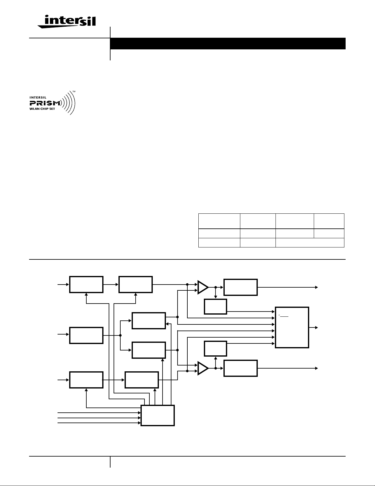
Functional Block Diagram
fIN IF
OSC
fIN RF
CLOCK
DAT A
LE
IN
IF
PRESCALER
OSC
RF
PRESCALER
15-BIT IF
N COUNTER
15-BIT IF
R COUNTER
15-BIT RF
R COUNTER
18-BIT RF
N COUNTER
22-BIT DATA
REGISTER
PHASE
COMP
PHASE
COMP
LD
RF
LD
CHARGE
PUMP
IF
f
OUT
LOCK
DETECT
FASTLOCK
MUX
CHARGE
PUMP
DO IF
FO/LD
DO RF
1
1-888-INTERSIL or 321-724-7143 | Intersil and Design is a trademark of Intersil Corporation. | Copyright © Intersil Corporation 2000
CAUTION: These devices are sensitive to electrostatic discharge; follow proper IC Handling Procedures.
PRISM® is a registered trademark of Intersil Corporation. PRISM logo is a trademark of Intersil Corporation.
Page 2
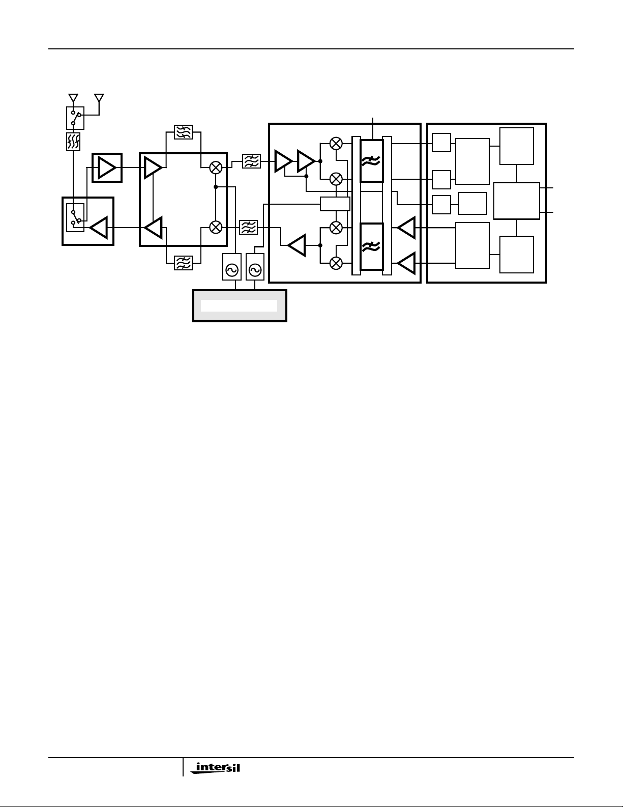
Typical Application Diagram
HFA3524
HF A3424 (NOTE)
(FILE# 4131)
HF A3624
UP/DOWN
CONVERTER
(FILE# 4066)
RFPA
HF A3925
(FILE# 4132)
HFA3524
NOTE: Required for systems targeting 802.11 specifications.
TYPICAL TRANSCEIVER APPLICATION CIRCUIT USING THE HFA352
VCO
VCO
DUAL SYNTHESIZER
(FILE# 4062)
HFA3724
(FILE# 4067)
÷2
QUAD IF MODULATOR
0o/90
TUNE/SELECT
I
M
o
U
X
Q
HSP3824
(FILE# 4064)
RXI
RXQ
RSSI
M
U
X
A/D
DE-
SPREAD
A/D
CCA
A/D
TXI
SPREAD
TXQ
DSSS BASEBAND PROCESSOR
PRISM CHIP SET FILE #4063
DPSK
DEMOD
802.11
MAC-PHY
INTERFACE
DPSK
MOD.
DATA TO MACCTRL
For additional information on the PRISM chip set, see us on
the web http://www.intersil.com/prism or call (321) 724-7800
to access Intersil’ AnswerFAX system. When prompted, key
in the four-digit document number (File #) of the datasheets
you wish to receive.
The four-digit file numbers are shown in Typical Application
Diagram, and correspond to the appropriate circuit.
2
Page 3
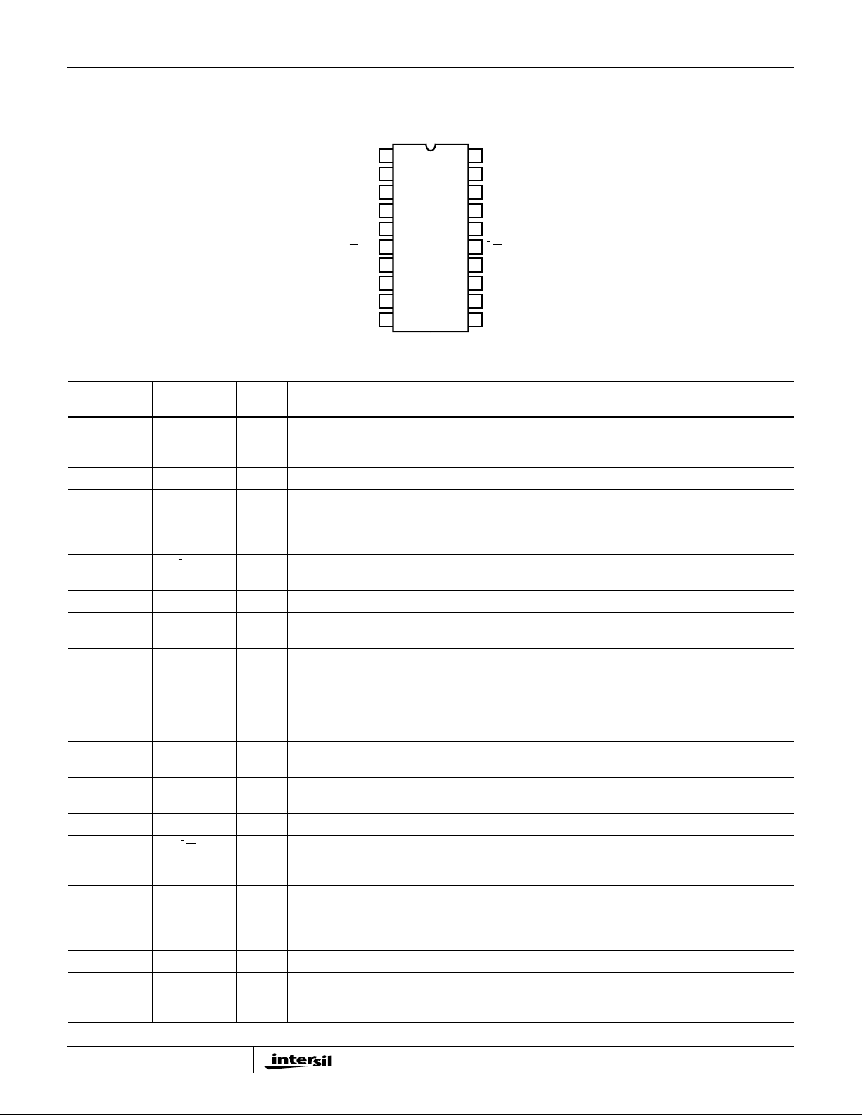
Pinout
HFA3524
HFA3524 (TSSOP)
TOP VIEW
V
CC1
V
DO RF
GND
f
RF
IN
fIN RF
GND
OSC
GND
/LD
F
O
1
2
P1
3
4
5
6
7
8
IN
9
10
20
19
18
17
16
15
14
13
12
11
V
CC2
V
P2
DO IF
GND
f
IF
IN
fIN IF
GND
LE
DAT A
CLOCK
Pin Descriptions
PIN
NUMBER PIN NAME I/O DESCRIPTION
1V
CC1
2VP1- Power Supply for RF charge pump. Must be > VCC.
3D
RF O Internal charge pump output. For connection to a loop filter for driving the input of an external VCO.
O
4 GND - Ground.
5f
RF I RF prescaler input. Small signal input from the VCO.
IN
6 fIN RF l RF prescaler complimentary input. A bypass capacitor should be placed as close as possible to this
7 GND - Ground.
8 OSC
IN
9 GND - Ground.
10 FO/LD O Multiplexed output of the RF/lF programmable or reference dividers, RF/lF lock detect signals and
11 Clock I High impedance CMOS Clock input. Data for the various counters is clocked in on the rising edge,
12 Data l Binary serial data input. Data entered MSB first. The last two bits are the control bits. High
13 LE l Load enable CMOS input. When LE goes HIGH, data stored in the shift registers is loaded into one
14 GND - Ground.
15 fIN IF I IF prescaler complimentary input. A bypass capacitor should be placed as close as possible to
16 fIN IF I IF prescaler input. Small signal input from the VCO.
17 GND - Ground.
18 DO IF O IF charge pump output. For connection to a loop filter for driving the input of an external VCO.
19 V
20 V
P2
CC2
- Power supply voltage input. Input may range from 2.7V to 5.5V. V
must equal V
CC1
capacitors should be placed as close aspossibletothispin and be connected directly to the ground
plane.
pin and be connected directly to the ground plane. Capacitor is optional with some loss of sensitivity.
I Oscillator input. The input has a VCC/2 input threshold and can be driven from an external CMOS
or TTL logic gate.
Fastlock mode. CMOS output (see Programmable Modes).
into the 22-bit shift register.
impedance CMOS input.
of the 4 appropriate latches (control bit dependent).
this pin and be connected directly to the ground plane. Capacitor is optional with some loss of
sensitivity.
- Power Supply for IF charge pump. Must be >VCC.
- Power supply voltage input Input may range from 2.7V to 5.5V. V
must equal V
CC2
capacitors should be placed as close as possible to this pin and be connected directly to the ground
plane.
CC2
CC1
. Bypass
. Bypass
3
Page 4
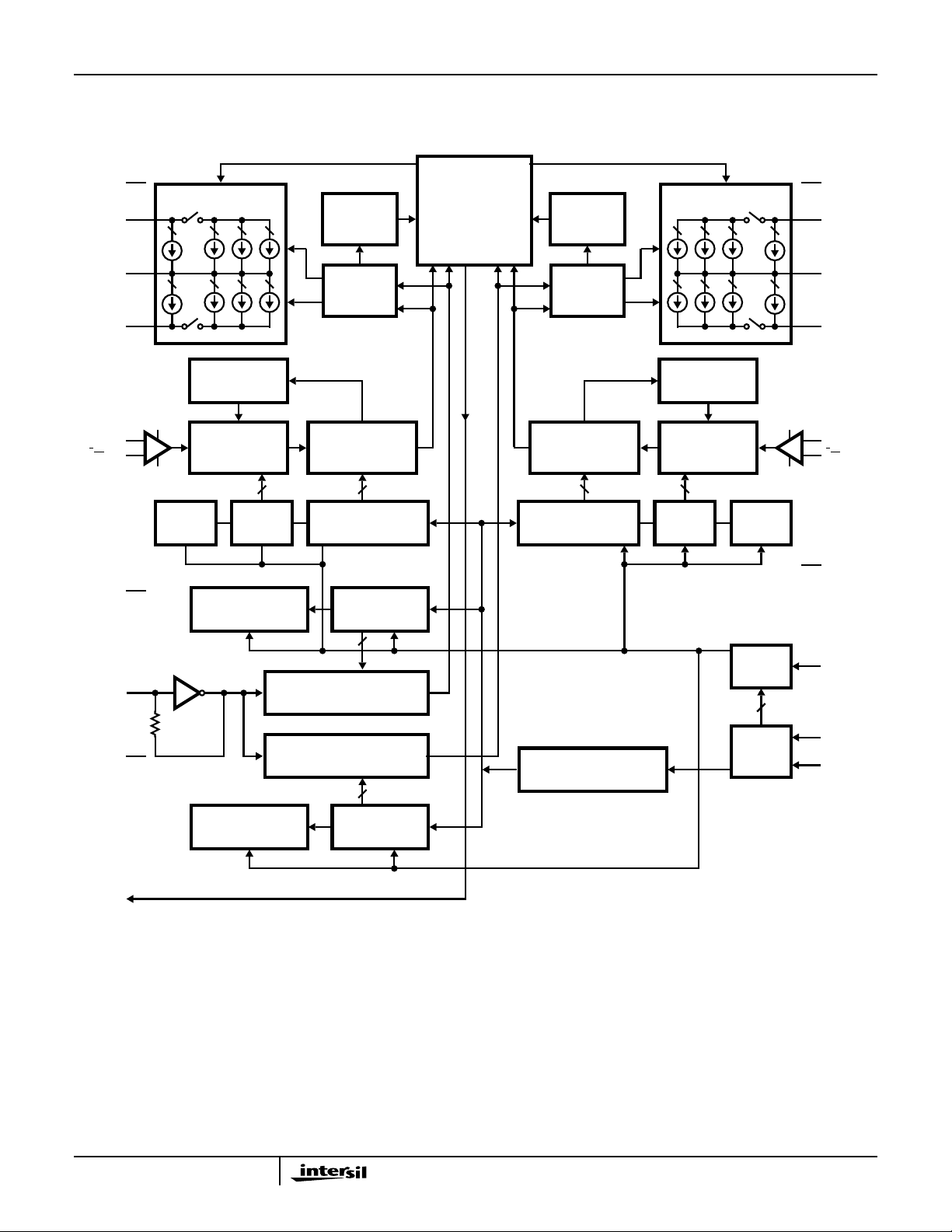
Block Diagram
HFA3524
V
CC1
V
DORF
GND
fIN RF
fIN RF
GND
1
2
P1
3
4
5
+
6
-
7
1X 4X
RF CHARGE PUMP
SWALLOW
CONTROL
32/33 OR 64/65
RF PRESCALER
1-BIT RF
PWDN
1-BIT P1
LATCH
RF
LOCK
DETECT
PU
RF
PHASE
PD
DETECTOR
PROGRAMMABLE
18-BIT (RF)
N-COUNTER
(RF) 18-BIT N-LATCH
15-BIT R1 LATCH5-BIT MODE LATCH
LOCK DETECT/
MULTIPLEXER
FR 1
FP 1
/
f
OUT
FASTLOCK
IF
LOCK
DETECT
FR 2
FP 2
(IF) 15-BIT N-LATCH
IF
PHASE
DETECTOR
PROGRAMMABLE
15-BIT (IF)
N-COUNTER
PU
PD
IF PRESCALER
1-BIT P2
LATCH
4X1X
IF CHARGE PUMP
SWALLOW
CONTROL
8/9 OR 16/17
1-BIT IF
PWDN
20
V
CC2
19
V
P2
18
DOIF
17
GND
16
fIN IF
+
15
-
fIN IF
14
GND
OSC
GND
F
O
8
IN
9
10
LD
PROGRAMMABLE 15-BIT
(R1) REFERENCE COUNTER
PROGRAMMABLE 15-BIT
(R2) REFERENCE COUNTER
15-BIT R2 LATCH5-BIT MODE LATCH
NOTES:
1. V
suppliespowerto the RF prescaler,N-counterand phase detector. V
CC1
RF and IF R-counters along with the OSCIN buffer and all digital circuitry. V
same voltage level.
2. VP1 and VP2 can be run independently as long as VP≥ VCC.
LATCH
DECODE
2-BIT
CONTROL
20-BIT SHIFT REGISTER
suppliespowerto the IF prescaler,N-counterand phase detector,
CC2
CC1
and V
are separated by a diode and must be run at the
CC2
LATCH
13
12
11
LE
DAT A
CLOCK
4
Page 5
HFA3524
Absolute Maximum Ratings Thermal Information
Power Supply Voltage
VCC . . . . . . . . . . . . . . . . . . . . . . . . . . . . . . . . . . . . -0.3V to +6.5V
VP. . . . . . . . . . . . . . . . . . . . . . . . . . . . . . . . . . . . . . -0.3V to +6.5V
Voltage on Any Pin with GND = 0V (VI). . . . . . . . . . . -0.3V to +6.5V
Operating Conditions
Power Supply Voltage
VCC . . . . . . . . . . . . . . . . . . . . . . . . . . . . . . . . . . . . . .2.7V to 5.5V
VP. . . . . . . . . . . . . . . . . . . . . . . . . . . . . . . . . . . . . . . . . . . .VCC to +5.5V
Temperature (TA) . . . . . . . . . . . . . . . . . . . . . . . . . . . . -40oC to 85oC
CAUTION: Stresses above those listed in “Absolute Maximum Ratings” may cause permanent damage to the device. This is a stress only rating and operation of the
device at these or any other conditions above those indicated in the operational sections of this specification is not implied.
NOTE:
3. θJA is measured with the component mounted on an evaluation PC board in free air.
Thermal Resistance (Typical, Note 3) θJA (oC/W)
TSSOP Package . . . . . . . . . . . . . . . . . . . . . . . . . . . 130
Maximum Storage Temperature Range (TS). . . . . . -55oC to 150oC
Maximum Lead Temperature (Soldering 4s) (TL) . . . . . . . . . .260oC
(TSSOP - Lead Tips Only)
Electrical Specifications V
= 3.0V, VP = 3.0V, -40oC < TA < 85oC, Unless Otherwise Specified
CC
HFA3524
PARAMETER SYMBOL TEST CONDITIONS
Power Supply Current I
CC
UNITSMIN TYP MAX
RF + IF VCC = 2.7V to 5.5V - 13 - mA
RF Only VCC = 2.7V to 5.5V - 10 - mA
Powerdown Current I
CC-PWDNVCC
= 3.0V - 1 25 µA
Operating Frequency fIN RF 0.5 - 2.5 GHz
Operating Frequency fIN IF 45 - 600 MHz
Oscillator Frequency f
Maximum Phase Detector
Frequency
OSC
f
φ
5 - 44 MHz
10 - - MHz
RF Input Sensitivity PfIN RF VCC = 3.0V -15 - +4 dBm
VCC = 5.0V -10 - +4 dBm
IF Input Sensitivity PfIN IF VCC = 2.7V to 5.5V -10 - +4 dBm
Oscillator Sensitivity V
High Level Input Voltage V
Low Level Input Voltage V
High Level Input Current I
Low Level Input Current I
Oscillator Input Current I
Oscillator Input Current I
High Level Output Voltage V
High Level Output Voltage V
Low Level Output Voltage V
Low Level Output Voltage V
Data to Clock Set Up Time t
Data to Clock Hold Time t
Clock Pulse Width High t
Clock Pulse Width Low t
Clock to Load Enable Set Up Time t
Load Enable Pulse Width t
OSC
IH
IL
IH
IL
IH
IL
OH
OH
OL
OL
CS
CH
CWH
CWL
ES
EW
OSC
IN
(Note) 0.8V
(Note) - - 0.2V
0.5 - - V
CC
-- V
CC
VIH = VCC = 5.5V (Note) -1.0 - 1.0 µA
VIL = 0V, VCC = 5.5V (Note) -1.0 - 1.0 µA
VIH = VCC = 5.5V - - 100 µA
VIL = 0V, VCC = 5.5V -100 - - µA
IOH = -500µAV
-0.4 - - V
CC
IOH = -1mA - - - V
IOL = 500µA - - 0.4 V
IOL = 1mA - - - V
See Data Input Timing 50 - - ns
See Data Input Timing 10 - - ns
See Data Input Timing 50 - - ns
See Data Input Timing 50 - - ns
See Data Input Timing 50 - - ns
See Data Input Timing 50 - - ns
NOTE: Clock, Data and LE does not include fIN RF, fIN IF and OSCIN.
P-P
V
5
Page 6

HFA3524
Charge Pump Specifications V
= 3.0V, VP = 3.0V, -40oC < TA < 85oC, Unless Otherwise Specified
CC
HFA3524
PARAMETER SYMBOL TEST CONDITIONS
Charge Pump Output Current I
Charge Pump High Z State Current I
CP Sink vs Source Mismatch (Note 5) I
DO-SOURCE
I
DO-SINK
I
DO-SOURCE
I
DO-SINK
DO-HIGH Z
DO-SINK
SOURCE
CP Current vs Voltage (Note 6) IDO vs V
vs I
VDO = VP/2, I
VDO = VP/2, I
VDO = VP/2, I
VDO = VP/2, I
= HIGH (Note 4) - -5.0 - mA
CPO
= HIGH (Note 4) - 5.0 - mA
CPO
= LOW (Note 4) - -1.25 - mA
CPO
= LOW (Note 4) - 1.25 - mA
CPO
0.5V ≤ VDO≤ VP - 0.5, -40oC < T < 85oC -2.5 - 2.5 nA
VDO = VP/2, TA = 25oC-310%
DO-
0.5V ≤ VDO≤ VP - 0.5, T < 25oC - 10 15 %
DO
UNITSMIN TYP MAX
CP Current vs Temperature (Note 7) IDO vs T VDO = VP/2, -40oC < T < 85oC-10-%
NOTES:
4. See Programmable Modes for I
description.
CPO
5. IDO vs VDO = Charge Pump Output Current magnitude variation vs Voltage =
[1/2 •{|I1| - |I3|}]/[1/2 • {|I1| + |I3|}] • 100% and [1/2 • |I4| - |I6|]/[1/2 • {|I4| + |I6|}] • 100%.
6. I
DO
-SINK
vs I
D
O-SOURCE
= Charge Pump Output Current Sink vs Source Mismatch = [|I2| - |I5|]/[1/2 • {|I2| + |I5|}] • 100%.
7. IDO vs TA = Charge Pump Output Current magnitude variation vs Temperature =
[|I2 at temp| - |I2 at 25oC|]/|I2 at 25oC| • 100% and [|I5 at temp| - |I5 at 25oC|]/ |I5 at 25oC| • 100%.
I1 = CP sink current at VDO = VP - ∆V
I2 = CP sink current at VDO = VP/2
I3 = CP sink current at VDO = ∆V
I4 = CP source current at VDO = VP - ∆V
I5 = CP source current at VDO = VP/2
I6 = CP source current at VDO = ∆V
FIGURE 1. CHARGE PUMP CURRENT SPECIFICATION DEFINITIONS
PARALLEL
PC
PORT
HP5385A
FREQUENCY
COUNTER
IN
39K
12K
2.2µF
CLOCK
DAT A
LE
FC
LD
F
O
100pF
I3
I2
I1
CURRENT (mA)
I4
I5
I6
0
f
IN
V
V
OSC
100pF
VOLTAGE
OFFSET ∆V
∆V
0Ω
CC
0.01µF
P
IN
2.2µF
100pF
51
VOLTAGE
D
O
VP/2
-∆V
V
P
13dB
ATTN
RF 50Ω
SMHU 835.8011.52
SIGNAL GENERATOR
10MHz EXT REF OUT
∆V
V
P
2.7V 5.0V
FIGURE 2. RF SENSITIVITY TEST BLOCK DIAGRAM
6
Page 7

Typical HFA3524 Performance Curves
HFA3524
15
14
13
12
11
(mA)
CC
I
10
9
8
7
2.5 3.0 3.5 4.0 4.5 5.0 5.5
T = 25oC
VCC (V)
FIGURE 3. ICC vs V
6
4
2
0
CURRENT (mA)
-2
O
D
-4
VP = 2.7V
T = 85oC
T = 40oC
CC
VP = 5.5V
VP = 5.5VVP = 2.7V
1500
1250
1000
750
500
250
HIGH Z STATE (pA)
DO
0
I
-250
-500
0123456
DO VOLTAGE (V)
T = 90oC
T = 70oC
T = 25oC
FIGURE 4. IDO HIGH Z STATE vs DO VOLTAGE
2.0
1.5
1.0
0.5
0
-0.5
CURRENT (mA)
O
D
-1.0
-1.5
VP = 2.7V
VP = 5.5V
VP = 5.5VVP = 2.7V
-6
0 0.5 1.0 1.5 2.0 2.5 3.0 3.5 4.0 4.5 5.0
DO VOLTAGE (V)
FIGURE 5. CHARGE PUMP CURRENT vs DO VOLTAGE
ICP = HIGH
25
20
15
VP = 3.0V
10
VARIATION (%)
5
0
0 0.25 0.5 0.75 1.0 1.25 1.5 1.75 2.0 2.25 2.5
VOLTAGE OFFSET (V)
VP = 5.0V
NOTE: See charge pump current specification definitions.
FIGURE 7. CHARGE PUMP CURRENT VARIATION
SINK
SOURCE
-2.0
0 0.5 1.0 1.5 2.0 2.5 3.0 3.5 4.0 4.5 5.5
DO VOLTAGE (V)
FIGURE 6. CHARGE PUMP CURRENT vs DO VOLTAGE
ICP = LOW
20
15
10
5
0
-5
-10
MISMATCH (%)
-15
-20
-25
0 0.5 1.0 1.5 2.0 2.5 3.0 3.5 4.0 4.5 5.0
FIGURE 8. SINK vs SOURCE MISMATCH vs D
VP = 3.0V
VOLTAGE (V)
D
O
VP = 5.0V
VOLTAGE
O
5.0
7
Page 8

HFA3524
Typical HFA3524 Performance Curves (Continued)
VCC = 2.7V TO 5.5V,
f
= 0.5GHz TO 3GHz
IN
3
2
Marker 1 = 1GHz, Real = 101, Imaginary = -144
Marker 2 = 2GHz, Real = 37, Imaginary = -54
Marker 3 = 3GHz, Real = 22, Imaginary = -2
Marker 4 = 500MHz, Real = 209, Imaginary = -232
FIGURE 9. RF INPUT IMPEDANCE
-10
-15
-20
-25
-30
-35
SENSITIVITY (dBm)
-40
-45
1000 1200 1400 1600 1800 2000 2200 2400 2600 2800 3000
VCC = 5.5V
VCC = 2.7V
FREQUENCY (MHz)
VCC = 2.7V TO 5.5V,
= 10MHz TO 1000MHz
f
IN
4
1
1
4
2
3
Marker 1 = 100MHz, Real = 589, Imaginary = -209
Marker 2 = 200MHz, Real = 440, Imaginary = -286
Marker 3 = 300MHz, Real = 326, Imaginary = -287
Marker 4 = 500MHz, Real = 202, Imaginary = -234
FIGURE 10. IF INPUT IMPEDANCE
-10
-15
-20
-25
-30
-35
SENSITIVITY (dBm)
-40
-45
-50
0 100 200 300 400 500 600
VCC = 5.5V
VCC = 2.7V
FREQUENCY (MHz)
FIGURE 11. RF SENSITIVITY vs FREQUENCY FIGURE 12. IF INPUT SENSITIVITY vs FREQUENCY
0
-10
-20
-30
-40
SENSITIVITY (dBm)
-50
-60
0 1020304050
VCC = 5.5V
VCC = 2.7V
FREQUENCY (MHz)
0.200
0.063
0.020
0.006
0.002
)
PP
SENSITIVITY (V
FIGURE 13. OSCILLATOR INPUT SENSITIVITY vs FREQUENCY
8
Page 9

Functional Description
The simplified block diagram in Figure 14 shows the 22-bit
data register,two 15-bit R Counters and the 15-bit and 18-bit
N Counters (intermediate latches are not shown). The data
stream is clocked (on the rising edge of Clock) into the DATA
input, MSB first. The last two bits are the Control Bus. The
DATA is transferred into the counters as follows:
fIN IF
OSC
IF
PRESCALER
IN
OSC
15-BIT IF
N COUNTER
15-BIT IF
R COUNTER
15-BIT RF
R COUNTER
HFA3524
PHASE
COMP
CONTROL BITS
0 0 IR R Counter
0 1 RF R Counter
1 0 IF N Counter
1 1 RF N Counter
CHARGE
PUMP
IF
LD
f
OUT
LOCK
DETECT
FASTLOCK
RF
LD
MUX
DATA LOCATIONC1 C2
DO IF
FO/LD
fIN RF
CLOCK
DAT A
LE
RF
PRESCALER
18-BIT RF
N COUNTER
22-BIT DATA
REGISTER
CHARGE
PUMP
PHASE
COMP
DO RF
FIGURE 14. SIMPLIFIED BLOCK DIAGRAM
Programmable Reference Dividers (IF and RF R Counters)
If the Control Bits are 00 or 01 (00 for IF and 01 for RF) data is transferred from the 22-bit shift register into a latch which sets the
15-bit R Counter. Serial data format is shown below.
LSB
↓
C1 C2 R1R2R3R4R5R6R7R8R9R10R11R12R13R14R15R16R17R18R19R
(Control bits)
Divide ratio of the reference divider, R Program Modes
15-BIT PROGRAMMABLE REFERENCE DIVIDER RATIO (R COUNTER)
DIVIDE
RATIO
3 000000000000011
4 000000000000100
• •••••••••••••••
32767 1 1 1 1 1 1 1 1 1 1 1 1 1 1 1
NOTES:
8. Divide ratios less than 3 are prohibited.
9. Divide ratio: 3 to 32767.
10. R1 to R15: These bits select the divide ratio of the programmable reference divider.
11. Data is shifted in MSB first.
15
R
R
14
13
R
12
R
11
R
10
R
R
9
R
8
R
7
R
6
R
5
R
4
R
3
MSB
↓
20
R
2
R
1
9
Page 10

HFA3524
Programmable Divide (N Counter)
The N counter consists of the 7-bit swallow counter (A counter) and the 11-bit programmable counter (B counter). If the Control
Bits are 10 or 11 (10 for IF counter and 11 for RF counter) data is transferred from the 22-bit shift register into a 4-bit or 7-bit latch
(which sets the Swallow (A) Counter) and an 11-bit latch (which sets the 11-bit programmable (B) Counter), MSB first. Serial data
format is shown below. For the IF N counter bits 5, 6, and 7 are don’t care bits. The RF N counter does not have don’t care bits.
LSB
↓
C1 C2 N1N2N3N4N5N6N7N8N9N10N11N12N13N14N15N16N17N18N19N
(Control bits) Divide ratio of the programmable divider, N Program
7-Bit Swallow Counter Divide Ratio (A Counter) Pulse Swallow Function
f
RF
DIVIDE
RATIO AN7
0 0000000
1 0000001
• •••••••
127 1111111
NOTES:
12. Divide ratio 0 to 127.
13. B ≥ A.
DIVIDE
RATIO AN7
0 XXX0000
1 XXX0001
• •••••••
15 X X X 1 1 1 1
X = Don’t care condition.
11-BIT PROGRAMMABLE COUNTER DIVIDE RATIO (B COUNTER
DIVIDE
RATIO BN18N17N16N15N14N13N12N11N10N9N8
3 00000000011
4 00000000100
• •••••••••••
2047 1 1 1 1 1 1 1 1 1 1 1
NOTES:
14. Divide ratio 3 to 2047 (divide ratios less than 3 are prohibited).
15. B ≥ A.
N
N
N
N
N
N
6
5
4
3
2
1
IF
N
N
N
N
N
N
6
5
4
3
2
1
= [(P x B) + A] x f
VCO
f
:Output frequency of external voltage controlled
VCO
oscillator (VCO)
B: Preset divide ratio of binary 11-bit programmable
counter (3 to 2047)
A: Preset divide ratio of binary 7-bit swallow counter
(0 ≤ A ≤ 127 {RF}, 0 ≤ A ≤ 15 {IF}, A ≤ B)
f
:Output frequency of the external reference frequency
OSC
oscillator
R: Preset divide ratio of binary 15-bit programmable
reference counter (3 to 32767)
P: Preset modulus of dual modulus prescaler
(for IF: P = 8 or 16; for RF: P = 32 or 64)
Programmable Modes
Several modes of operation can be programmed with bits
R16-R19 including the phase detector polarity, charge pump
High Z State and the output of the F
and powerdown modes are selected with bits N19 and N20.
The programmable modes are shown in Table 1. Truth table
forthe programmable modes and F
Table 2 and Table 3.
TABLE 1. PROGRAMMABLE MODES
C1 C2 R16 R17 R18 R19 R20
0 0 IF Phase
Detector Polarity
0 1 RF Phase
Detector Polarity
C1 C2 N19 N20
1 0 IF Prescaler Powerdown IF
1 1 RF Prescaler Powerdown RF
OSC
/R
IF I
RF I
/LD pin. The prescaler
O
/LD output are shown in
O
IF D
CPO
CPO
O
High Z
RF D
High Z
O
IF LD IF F
RF LD RF F
MSB
↓
20
O
O
10
Page 11

HFA3524
TABLE 2. MODE SELECT TRUTH TABLE
ΦD
POLARITY DO HIGH Z STATE
0 Negative Normal Operation LOW 8/9 32/33 Powered Up
1 Positive High Z State HIGH 16/17 64/65 Powered Down
NOTES:
16. The I
17. Activation of the IF PLL or RF PLL powerdown modes result in the disabling of the respective N counter divider and debiasing of its respective
fINinputs (to a high impedance state). Powerdown forces the respective charge pump and phase comparator logic to a High Z State condition.
The R counter functionality does not become disabled until both IF and RF powerdown bits are activated. The OSCIN pin reverts to a high impedance state when this condition exists. The control register remains active and capable of loading and latching in data during all of the powerdown modes.
X = Don’t care condition
NOTES:
18. When the FO/LD output is disabled, it is actively pulled to a low logic state.
19. Lock detect output provided to indicate when the VCO frequency is in “lock”. When the loop is locked and a lock detect mode is selected, the
pins output is HIGH, with narrow pulses LOW. In the RF/IF lock detect mode a locked condition is indicated when RF and IF are both locked.
20. The Fastlock mode utilizes the FO/LD output pin to switch a second loop filter damping resistor to ground during fastlock operation. Activation
of Fastlock occurs whenever the RF loop’s lcpo magnitude bit #17 is selected HIGH (while the #19 and #20 mode bits are set for Fastlock).
21. The Counter Reset mode bits R19 and R20 when activated reset all counters. Upon removal of the Reset bits, the N counter resumes counting
in “close” alignment with the R counter. (The maximum error is one prescaler cycle.) If the Reset bits are activated, the R counter is also forced
to Reset, allowing smooth acquisition upon powering up.
LOW current state = 1/4 x I
CPO
RF R [19]
(RF LD)
0000Disabled (Note 18)
0100IF Lock Detect (Note 19)
1000RF Lock Detect (Note 19)
1100RF/IF Lock Detect (Note 19)
X 0 0 1 IF Reference Divider Output
X 0 1 0 RF Reference Divider Output
X 1 0 1 IF Programmable Divider Output
X 1 1 0 RF Programmable Divider Output
0011Fastlock (Note 20)
0111For Internal Use Only
1011For Internal Use Only
1111For Internal Use Only
1111Counter Reset (Note 21)
IF R [19]
(IF LD)
HIGH current.
CPO
TABLE 3. THE FO/LD (PIN 10) OUTPUT TRUTH TABLE
(NOTE 16)
I
CPO
RF R [20]
(RF FO)
IF
PRESCALER
IF R [20]
(IF FO)F
RF
PRESCALER
O
(NOTE 17)
POWERDOWN
OUTPUT STATE
Phase Detector Polarity
Depending upon VCO characteristics, R16 bit should be set
accordingly, (see Figure 15).
• When VCO characteristics are positive like (1), R16
should be set HIGH.
• When VCO characteristics are negative like (2), R16
should be set LOW.
11
(1)
(2)
VCO OUTPUT FREQUENCY
VCO INPUT VOLTAGE
FIGURE 15. VCO CHARACTERISTICS
Page 12

HFA3524
DAT A
CLOCK
OR
LE
LE
N20: MSB
(R20: MSB)
t
CS
N19
(R19)
N10 N9 N1 CONTROL BIT: LSB
(R8) (R7) (R6) (R1) CONTROL BIT: LSB
t
CWL
t
CH
t
CWH
t
ES
t
EW
NOTES:
22. Parenthesis data indicates programmable reference divider data.
23. Data shifted into register on clock rising edge.
24. Data is shifted in MSB first.
Test Conditions: The Serial Data Input Timing is tested using a symmetrical waveform around VCC/2. The test waveform has an edge rate of
0.6V/ns with amplitudes of 2.2V at VCC = 2.7V and 2.6V at VCC = 5.5V.
FIGURE 16. SERIAL DATA INPUT TIMING
f
R
f
P
LD
D
O
fR > f
H
P
fR = f
P
Z
II I
L
fR < f
P
fR < f
P
fR < f
NOTES:
25. Phase difference detection range: -2π to +2π
26. The minimum width pump up and pump down current pulses occur at the DO pin when the loop is locked.
27. R16 = HIGH.
FIGURE 17. PHASE COMPARATOR AND INTERNAL CHARGE PUMP CHARACTERISTICS
P
12
Page 13

Typical Application Example
V
P
100pF
0.01µF
V
CC
100pF
100pF
0.01µF
V
CCVP
20 19 18 17 16 15 14 13 12 11
12345678910
CCVP
V
V
0.01µF
0.01µF
CC
P
C3
DO IF GND fIN IF
100pF
R2
C4
HFA3524
GNDDO RFV
HFA3524
VCO
(NOTE 28)
RIN (NOTE 29)
100pF
fIN IF
fIN RFfIN RF
100pF
R
IN
(NOTE 29)
GND
GND
OSC
100pF
10pF
DAT ALE
CLOCK
GND F
IN
CRYSTAL OSCILLATOR
INPUT
51Ω
(NOTE 30)
O
/LD
IF OUT
F
FROM
CONTROLLER
/LD
O
10pF
RF OUT
C1
VCO
(NOTE 28)
R1
C2
NOTES:
28. VCO is assumed AC coupled.
29. RINincreases impedance so that VCO output power is provided to the load rather than the PLL. Typical values are 10Ω to 200Ω depending on
the VCO power level. fIN RF impedance ranges from 40Ω to 100Ω. fIN IF impedances are higher.
30. 50Ω termination is often used on test boards to allow use of external reference oscillator. For most typical products a CMOS clock is used and
no terminating resistor is required. OSCINmay be AC or DC coupled. AC coupling is recommended because the input circuit provides its own
bias (see Figure 16).
31. Proper use of grounds and bypass capacitors is essential to achieve a high level of performance. Crosstalk between pins can be reduced by
careful board layout.
32. This is a static sensitive device. It should be handled only at static free work stations.
FIGURE 18.
V
CC
OSC
IN
100kΩ
LD
FIGURE 19.
33K
100K
0.01µF
MMBT200
LOCK
DETECT
10K
Typical Locked Detect Circuit
A lock detect circuit is needed in order to provide a steady
LOW signal when the PLL is in the locked state. A typical circuit is shown in Figure 20.
13
FIGURE 20.
Page 14

CRYSTAL
REFERENCE
1/R
REFERENCE
DIVIDER
f
R
f
P
PHASE
DETECTOR
Φ
HFA3524
CHARGE
φ
R
φ
P
PUMP
V
P
LOOP
D
FILTER
O
Z(s)
VCO
f
OUT
REFERENCE
FREQUENCY
SYNTHESIZER
FREQUENCY
f
REF
FIGURE 21. BASIC CHARGE PUMP PHASE LOCKED LOOP
Application Information
A block diagram of the basic phase locked loop is shown in
Figure 21.
Loop Gain Equations
A linear control system model of the phase feedback for a
PLL in the locked state is shown in Figure 22. The open loop
gain is the product of the phase comparator gain (Kφ), the
VCO gain (K
the gain of the feedback counter modulus (N). The passive
loop filter configuration used is displayed in Figure 23, while
the complex impedance of the filter is given in Equation 2.
Θ
R
/s), and the loop filter gain Z(s) divided by
VCO
Θ
E
∑
+
-
Θ
I
K
Z(s)
φ
1/N
K
FIGURE 22. PLL LINEAR MODEL
VCO
s
Θ
O
f
1/N
MAIN
DIVIDER
IN
The 3rd order PLL Open Loop Gain can be calculated in
terms of frequency, ω, the filter time constants T1 and T2,
and the design constants K
Kφ K
Gs() Hs()•
s= j w•
------------------------------------------------------------------ -
ω2C1 N 1 jω T1•+()•
φ, KVCO
VCO
, and N.
1jω T2•+()•–
T1
------ -
•=
T2
From Equation 3 we can see that the phase term will be
dependent on the single pole and zero such that the phase
margin is determined in Equation 5.
1–
φω() tan
ω T2•()tan1–ω T1•()– 180o+=
A plot of the magnitude and phase of G(s)H(s) for a stable
loop, is shown in Figure 24 with a solid trace. The parameter
φ
shows the amount of phase margin that exists at the point
P
the gain drops below zero (the cutoff frequency wp of the
loop). In a critically damped system, the amount of phase
margin would be approximately 45 degrees.
(EQ. 4)
(EQ. 5)
O
C1
VCOD
R2
C2
FIGURE 23. PASSIVE LOOP FILTER
VCO
⁄==
IΘE
Ns⁄=
(EQ. 1)
(EQ. 2)
Open loop gain H(s) G(s) Θ
Z(s) K
K
φ
Zs()
sC2 R2•()1+
---------------------------------------------------------------------------------- -=
2
C1 C2 R2••()sC1 sC2++
s
The time constants which determine the pole and zero
frequencies of the filter transfer function can be defined as:
T1 R2
----------------------
•=
C1 C2+
(EQ. 3A)
C1 C2•
and
T2 R2 C2•=
(EQ. 3B)
14
If we were now to redefine the cut off frequency, wp’, as
double the frequency which gave us our original loop
bandwidth, wp, the loop response time would be
approximately halved. Because the filter attenuation at the
comparison frequency also diminishes, the spurs would have
increased by approximately 6dB. In the proposed Fastlock
scheme, the higher spur levels and wider loop filter conditions
would exist only during the initial lock-on phase - just long
enough to reap the benefits of locking faster. The objective
would be to open up the loop bandwidth but not introduce any
additional complications or compromises related to our
original design criteria. We would ideally like to momentarily
shift the curve of Figure 24 overto a different cutoff frequency,
illustrated by the dotted line, without affectingthe relative open
loop gain and phase relationships. To maintain the same
gain/phase relationship at twice the original cutoff frequency,
other terms in the gain and phase Equations 4 and 5 will have
to compensate by the corresponding “1/w” or 1/w
2
” factor .
Examination of Equations 3 and 5 indicates the damping
resistor variable R2 could be chosen to compensate the “w”
terms for the phase margin. This implies that another resistor
Page 15

HFA3524
of equal value to R2 will need to be switched in parallel with
R2 during the initial lock period. We must also insure that the
magnitude of the open loop gain, H(s)G(s) is equal to zero at
wp’ = 2wp. K
be changed by a factorof 4, to counteract the w
,Kφ, N, or the net product of these terms can
VCO
2
term present
in the denominator of Equation 3. The Kφ term was chosen to
complete the transformation because it can readily be
switched between 1X and 4X values. This is accomplished by
increasing the charge pump output current from 1mA in the
standard mode to 4mA in Fastlock.
Fastlock Circuit Implementation
A diagram of the Fastlockscheme as implemented in Intersil
Corporations HFA3524 PLL is shown in Figure 25. When a
new frequency is loaded, and the RF Icp
charge pump circuit receives an input to deliver 4 times the
GAIN
|<G(s) H(s)|
0dB
bit is set high, the
O
ω
P
normal current per unit phase error while an open drain
NMOS on chip device switches in a second R2 resistor
element to ground. The user calculates the loop filter
component values for the normal steady state
considerations. The device configuration ensures that as
long as a second identical damping resistor is wired in
appropriately, the loop will lock faster without any additional
stability considerations to account for. Once locked on the
correct frequency, the user can return the PLL to standard
low noise operation by sending an instruction with the RF
Icp
bit set low. This transition does not affect the charge on
O
the loop filter capacitors and is enacted synchronous with
the charge pump output. This creates a nearly seamless
change between Fastlock and standard mode.
PHASE
G(s) H(s)
ω
= 2ω
’
P
P
-90
φ
P
FREQUENCY
φ
’
P
-180
FIGURE 24. OPEN LOOP RESPONSE BODE PLOT
CRYSTAL
REFERENCE
1/R
REFERENCE
DIVIDER
DIVIDER MAIN
PHASE
DETECTOR
f
P
Φ
f
R
FASTLOCK
1/N
CHARGE
PUMP
φ
R
φ
P
1X 4X
f
IN
V
P
C2
R2
VCO
RF
OUT
O
LD
LOOP FILTER
C1
R2’
D
F
O
FIGURE 25. FASTLOCK CIRCUIT IMPLEMENTATION
All Intersil semiconductor products are manufactured, assembled and tested under ISO9000 quality systems certification.
Intersil semiconductor products are sold by description only.Intersil Corporation reserves the right to make changes in circuit design and/or specifications at any time without notice. Accordingly,the reader is cautioned to verify that data sheets are current before placing orders. Information furnished by Intersil is believed to be accurate and
reliable. However, no responsibility is assumed by Intersil or its subsidiaries for its use; nor for any infringements of patents or other rights of third parties which may result
from its use. No license is granted by implication or otherwise under any patent or patent rights of Intersil or its subsidiaries.
For information regarding Intersil Corporation and its products, see web site www.intersil.com
15
 Loading...