

Page 1
March 1997
HFA1109
450MHz, Low Power, Current Feedback
Video Operational Amplifier
Features
• Wide - 3dB Bandwidth (AV = +2). . . . . . . . . . . . 450MHz
• Gain Flatness (To 250MHz) . . . . . . . . . . . . . . . . . . 0.8dB
• Very Fast Slew Rate (A
• High Input Impedance . . . . . . . . . . . . . . . . . . . . . 1.7MΩ
• Differential Gain/Phase . . . . . . . . . 0.02%/0.02 Degrees
• Low Supply Current . . . . . . . . . . . . . . . . . . . . . . . 10mA
= +2). . . . . . . . . . . . . 1100V/µs
V
Applications
• Professional Video Processing
• Video Switchers and Routers
• Medical Imaging
• PC Multimedia Systems
• Video Distribution Amplifiers
• Flash Converter Drivers
• Radar/IF Processing
Description
The HFA1109 is a high speed, low power, current feedback
amplifier built with Intersil’s proprietary complementary bipolar UHF-1 process. This amplifier features a unique combination of power and performance specifically tailored for
video applications.
The HFA1109 is a standard pinout op amp. It is a higher
performance, drop-in replacement (no feedback resistor
change required) for the CLC409.
If a comparably performing op amp with an output disable
function (useful for video multiplexing) is required, please
refer to the HFA1149 data sheet.
Ordering Information
PART NUMBER
(BRAND)
HFA1109IP -40 to 85 8 Ld PDIP E8.3
HFA1109IB (H1109) -40 to 85 8 Ld SOIC M8.15
HFA11XXEVAL DIP Evaluation Board for High Speed
TEMP.
RANGE (oC) PACKAGE
Op Amps
PKG.
NO.
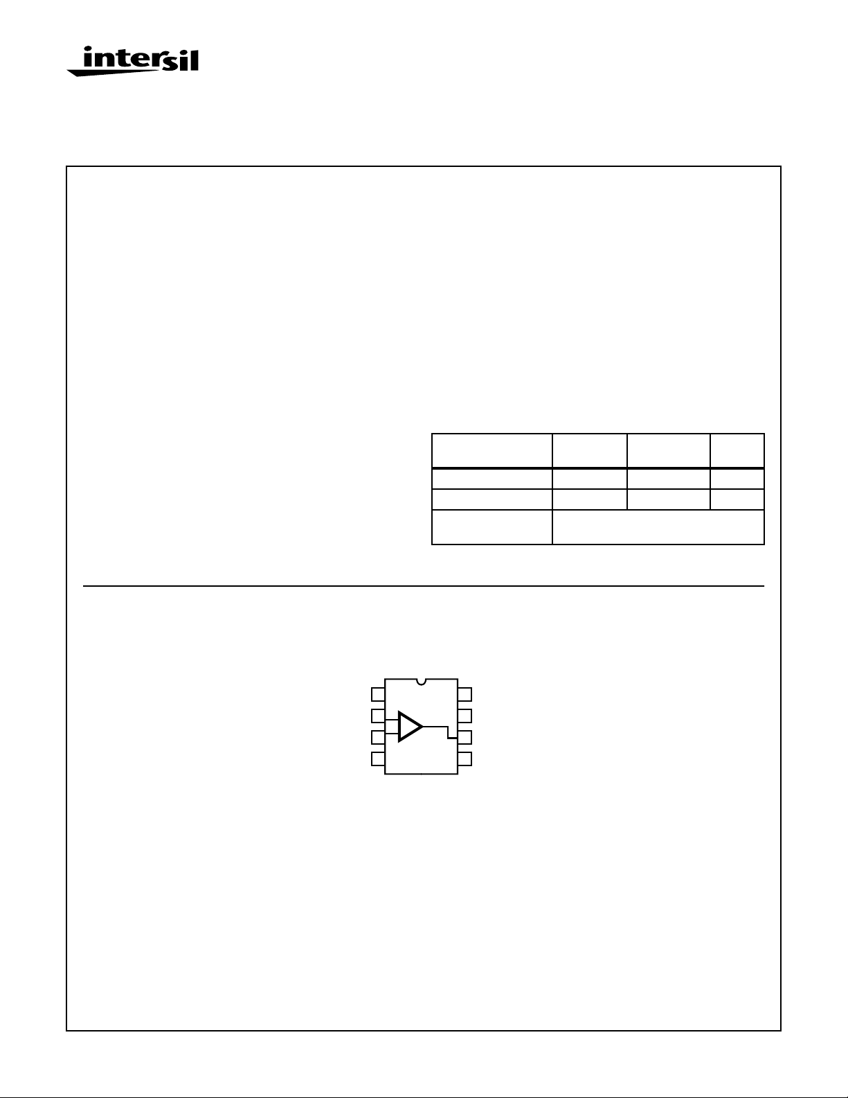
Pinout
NC
-IN
+IN
V-
HFA1109
(PDIP, SOIC)
TOP VIEW
1
2
+
3
4
8
NC
7
V+
6
OUT
5
NC
CAUTION: These devices are sensitive to electrostatic discharge; follow proper IC Handling Procedures.
1-888-INTERSIL or 321-724-7143 | Copyright © Intersil Corporation 1999
1
File Number 4019.3
Page 2

HFA1109
Absolute Maximum Ratings Thermal Information
Voltage Between V+ and V- . . . . . . . . . . . . . . . . . . . . . . . . . . . . 12V
DC Input Voltage . . . . . . . . . . . . . . . . . . . . . . . . . . . . . . . . V
SUPPLY
Differential Input Voltage. . . . . . . . . . . . . . . . . . . . . . . . . . . . . . . . 8V
Output Current (Note 2) . . . . . . . . . . . . . . . . Short Circuit Protected
30mA Continuous
60mA ≤ 50% Duty Cycle
ESD Rating
Human Body Model (Per MIL-STD-883 Method 3015.7) . . 1400V
Charged Device Model (Per EOS/ESD DS5.3, 4/14/93). . . 2000V
Machine Model (Per EIAJ ED-4701Method C-111) . . . . . . . . 50V
Operating Conditions
Temperature Range . . . . . . . . . . . . . . . . . . . . . . . . . -40oC to 85oC
CAUTION: Stresses above those listed in “Absolute Maximum Ratings” may cause permanent damage to the device. This is a stress only rating and operation
of the device at these or any other conditions above those indicated in the operational sections of this specification is not implied.
NOTES:
1. θJA is measured with the component mounted on an evaluation PC board in free air.
2. Output is short circuit protected to ground. Brief short circuits to ground will not degrade reliability, however continuous (100% duty cycle)
output current must not exceed 30mA for maximum reliability.
Thermal Resistance (Typical, Note 1) θJA (oC/W)
PDIP Package. . . . . . . . . . . . . . . . . . . . . . . . . . . . . 130
SOIC Package. . . . . . . . . . . . . . . . . . . . . . . . . . . . . 170
Maximum Junction Temperature (Die). . . . . . . . . . . . . . . . . . . . 175oC
Maximum Junction Temperature (Plastic Package) . . . . . . . . 150oC
Maximum Storage Temperature Range . . . . . . . . . -65oC to 150oC
Maximum Lead Temperature (Soldering 10s) . . . . . . . . . . . . 300oC
(SOIC - Lead Tips Only)
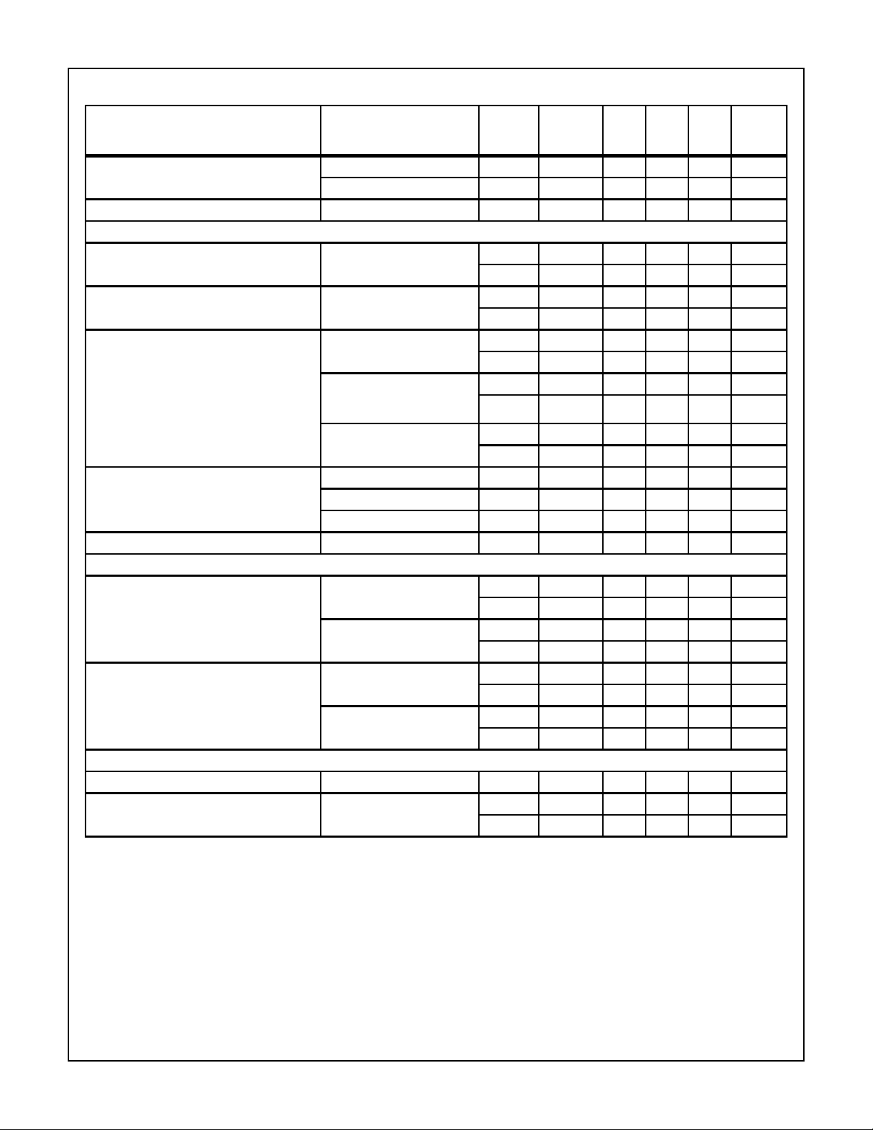
Electrical Specifications V
= ±5V, AV= +2, RF= 250Ω, RL = 100Ω, Unless Otherwise Specified
SUPPLY
(NOTE 3)
PARAMETER TEST CONDITIONS
TEST
LEVEL
TEMP.
(oC) MIN TYP MAX UNITS
INPUT CHARACTERISTICS
Input Offset Voltage A 25 - 1 5 mV
A Full - 2 8 mV
Average Input Offset Voltage Drift B Full - 10 - µV/oC
Input Offset Voltage
Common-Mode Rejection Ratio
Input Offset Voltage
Power Supply Rejection Ratio
∆V
= ±2V A 25 47 50 - dB
CM
= ±2V A Full 45 48 - dB
∆V
CM
= ±1.25V A 25 50 53 - dB
∆V
PS
∆V
= ±1.25V A Full 47 51 - dB
PS
Non-Inverting Input Bias Current A 25 - 4 10 µA
A Full - 5 15 µA
Non-Inverting Input Bias Current Drift B Full - 30 - nA/
Non-Inverting Input Bias Current
Power Supply Sensitivity
= ±1.25V A 25 - 0.5 1 µA/V
∆V
PS
∆V
= ±1.25V A Full - 0.5 3 µA/V
PS
Inverting Input Bias Current A 25 - 2 10 µA
A Full - 3 15 µA
Inverting Input Bias Current Drift B Full - 40 - nA/
Inverting Input Bias Current
Common-Mode Sensitivity
Inverting Input Bias Current
Power Supply Sensitivity
Non-Inverting Input Resistance ∆V
= ±2V A 25 - 3 6 µA/V
∆V
CM
= ±2V A Full - 3 8 µA/V
∆V
CM
= ±1.25V A 25 - 1.6 5 µA/V
∆V
PS
= ±1.25V A Full - 1.6 8 µA/V
∆V
PS
= ±2V A 25, 85 0.8 1.7 - MΩ
CM
= ±2V A -40 0.5 1.4 - MΩ
∆V
CM
Inverting Input Resistance B 25 - 60 - Ω
Input Capacitance B 25 - 1.6 - pF
o
C
o
C
2
Page 3

HFA1109
Electrical Specifications V
= ±5V, AV= +2, RF= 250Ω, RL = 100Ω, Unless Otherwise Specified (Continued)
SUPPLY
(NOTE 3)
PARAMETER TEST CONDITIONS
Input Voltage Common Mode Range
(Implied by VIO CMRR, +RIN, and -I
TEST
LEVEL
A Full ±2 ±2.5 - V
BIAS
TEMP.
(oC) MIN TYP MAX UNITS
CMS tests)
Input Noise Voltage Density (Note 4) f = 100kHz B 25 - 4 - nV/√
Non-Inverting Input Noise Current Density
f = 100kHz B 25 - 2.4 - pA/√
(Note 4)
Inverting Input Noise Current Density
f = 100kHz B 25 - 40 - pA/√
(Note 4)
TRANSFER CHARACTERISTICS
Open Loop Transimpedance Gain (Note 4) B 25 - 500 - kΩ
Minimum Stable Gain B Full - 1 - V/V
AC CHARACTERISTICS
-3dB Bandwidth
= 0.2V
(V
OUT
P-P
, Note 4)
AV = -1, RF = 200Ω B 25 300 375 - MHz
B Full 290 360 - MHz
= +1, +RS = 550Ω(PDIP),
A
V
+RS = 700Ω (SOIC)
B 25 280 330 - MHz
B Full 260 320 - MHz
AV = +2 B 25 390 450 - MHz
B Full 350 410 - MHz
Gain Peaking A
= +2, V
V
OUT
= 0.2V
P-P
B 25 - 0 0.2 dB
B Full - 0 0.5 dB
Gain Flatness
= +2, V
(A
V
OUT
= 0.2V
P-P
, Note 4)
To 125MHz B 25 -1.0 -0.45 - dB
B Full -1.1 -0.45 - dB
To 200MHz B 25 -1.6 -0.75 - dB
B Full -1.7 -0.75 - dB
To 250MHz B 25 -1.9 -0.85 - dB
B Full -2.2 -0.85 - dB
Gain Flatness
= +1, +RS = 550Ω (PDIP),
(A
V
+RS = 700Ω (SOIC), V
Note 4)
OUT
= 0.2V
P-P
,
To 125MHz B 25 ±0.3 ±0.1 - dB
B Full ±0.4 ±0.1 - dB
To 200MHz B 25 ±0.8 ±0.35 - dB
B Full ±0.9 ±0.35 - dB
To 250MHz B 25 ±1.3 ±0.6 - dB
B Full ±1.4 ±0.6 - dB
OUTPUT CHARACTERISTICS
Output Voltage Swing, Unloaded
(Note 4)
Output Current
(Note 4)
Output Short Circuit Current A
Closed Loop Output Resistance (Note 4) DC, A
Second Harmonic Distortion
(V
OUT
= 2V
P-P
, Note 4)
= -1, RL = ∞ A25±3 ±3.2 - V
A
V
A Full ±2.8 ±3- V
AV = -1, RL = 75Ω A 25, 85 ±33 ±36 - mA
A -40 ±30 ±33 - mA
= -1 B 25 - 120 - mA
V
= +1 B 25 - 0.05 - Ω
V
20MHz B 25 - -55 - dBc
60MHz B 25 - -57 - dBc
Hz
Hz
Hz
3
Page 4
HFA1109
Electrical Specifications V
= ±5V, AV= +2, RF= 250Ω, RL = 100Ω, Unless Otherwise Specified (Continued)
SUPPLY
(NOTE 3)
PARAMETER TEST CONDITIONS
Third Harmonic Distortion
(V
OUT
= 2V
P-P
, Note 4)
TEST
LEVEL
20MHz B 25 - -68 - dBc
60MHz B 25 - -60 - dBc
TEMP.
(oC) MIN TYP MAX UNITS
Reverse Isolation (S12) 30MHz B 25 - -65 - dB
TRANSIENT CHARACTERISTICS
Rise and Fall Times V
OUT
= 0.5V
P-P
B 25 - 1.1 1.3 ns
B Full - 1.1 1.4 ns
Overshoot V
OUT
= 0.5V
P-P
B25-02%
B Full - 0.5 5 %
Slew Rate AV = -1, RF= 200Ω
V
= 5V
A
OUT
V
= +1, V
P-P
OUT
= 4V
+RS = 550Ω (PDIP),
+RS = 700Ω (SOIC)
A
= +2, V
V
OUT
= 5V
P-P
P-P
,
B 25 2300 2600 - V/µs
B Full 2200 2500 - V/µs
B 25 475 550 - V/µs
B Full 430 500 - V/µs
B 25 940 1100 - V/µs
B Full 800 950 - V/µs
Settling Time
= +2V to 0V step, Note 4)
(V
OUT
To 0.1% B 25 - 19 - ns
To 0.05% B 25 - 23 - ns
To 0.01% B 25 - 36 - ns
Overdrive Recovery Time V
= ±2V B 25 - 5 - ns
IN
VIDEO CHARACTERISTICS
Differential Gain
(f = 3.58MHz)
= 150Ω B 25 - 0.02 0.06 %
R
L
B Full - 0.03 0.09 %
= 75Ω B 25 - 0.04 0.09 %
R
L
B Full - 0.05 0.12 %
Differential Phase
(f = 3.58MHz)
RL = 150Ω B 25 - 0.02 0.06 Degrees
B Full - 0.02 0.06 Degrees
RL = 75Ω B 25 - 0.05 0.09 Degrees
B Full - 0.06 0.13 Degrees
POWER SUPPLY CHARACTERISTICS
Power Supply Range C 25 ±4.5 - ±5.5 V
Power Supply Current (Note 4) A 25 - 9.6 10 mA
A Full - 10 11 mA
NOTES:
3. Test Level: A. Production Tested; B. Typical or Guaranteed Limit Based on Characterization; C. Design Typical for Information Only.
4. See Typical Performance Curves for more information.
4
Page 5

HFA1109
Application Information
Optimum Feedback Resistor
Although a current feedback amplifier’s bandwidth dependency on closed loop gain isn’t as severe as that of a v oltage
feedback amplifier, there can be an appreciable decrease in
bandwidth at higher gains. This decrease may be minimized
by taking advantage of the current feedback amplifier’s
unique relationship between bandwidth and R
feedback amplifiers require a feedback resistor, even for
unity gain applications, and R
, in conjunction with the inter-
F
nal compensation capacitor, sets the dominant pole of the
frequency response. Thus, the amplifier’s bandwidth is
inversely proportional to R
mized for a 250Ω R
. The HFA1109 design is opti-
F
at a gain of +2. Decreasing R
F
decreases stability, resulting in excessive peaking and overshoot (Note: Capacitive feedback will cause the same problems due to the feedback impedance decrease at higher
frequencies). At higher gains the amplifier is more stable, so
R
can be decreased in a trade-off of stability for bandwidth.
F
TABLE 1. OPTIMUM FEEDBACK RESISTOR
GAIN (ACL)R
-1 200 400
+1 250 (+RS= 550Ω) PDIP
250 (+RS= 700Ω) SOIC
+2 250 450
+5 100 160
+10 90 70
Table 1 lists recommended R
(Ω) BANDWIDTH (MHz)
F
values, and the expected
F
bandwidth, for various closed loop gains. For a gain of +1, a
resistor (
+R
) in series with +IN is required to reduce gain
S
peaking and increase stability
. All current
F
350
ble oscillations. In most cases, the oscillation can be avoided
by placing a resistor (R
) in series with the output prior to
S
the capacitance.
R
and CL form a low pass network at the output, thus limit-
S
ing system bandwidth well below the amplifier bandwidth. By
decreasing R
as CL increases, the maximum bandwidth is
S
obtained without sacrificing stability. In spite of this, bandwidth still decreases as the load capacitance increases.
Evaluation Board
The performance of the HFA1109 may be evaluated using
the HFA11XX evaluation board (part number
HFA11XXEVAL). Please contact your local sales office for
F
information. When evaluating this amplifier, the two 510Ω
gain setting resistors on the evaluation board should be
changed to 250Ω.
The layout and schematic of the board are shown in Figure 1.
.
510Ω
50Ω
IN
0.1µF10µF
BOARD SCHEMATIC
510Ω
1
2
3
4
-5V
TOP LAYOUT
GND
V
H
8
7
50Ω
6
5
OUT
V
GND
10µF0.1µF
+5V
L
PC Board Layout
The frequency response of this amplifier depends greatly on
the care taken in designing the PC board. The use of low
inductance components such as chip resistors and chip
capacitors is strongly recommended, while a solid ground
plane is a must! Attention should be given to decoupling the
power supplies. A large value (10µF) tantalum in par allel with a
small value (0.1µF) chip capacitor works well in most cases.
Terminated microstr ip signal lines are recommended at the
input and output of the device. Capacitance directly on the
output must be minimized, or isolated as discussed in the
next section.
Care must also be taken to minimize the capacitance to ground
seen by the amplifier’s inverting input (-IN). The larger this
capacitance, the worse the gain peaking, resulting in pulse
overshoot and possible instability. Thus it is recommended that
the ground plane be removed under traces connected to -IN,
and connections to -IN should be kept as short as possible.
Driving Capacitive Loads
Capacitive loads, such as an A/D input, or an improperly terminated transmission line will degrade the amplifier’s phase
margin resulting in frequency response peaking and possi-
V
H
1
+IN
OUT
V
BOTTOM LAYOUT
FIGURE 1. EVALUATION BOARD SCHEMATIC AND LAYOUT
V+
L
V-
GND
5
Page 6

HFA1109
Typical Performance Curves V
200
AV = +2
150
100
50
0
-50
OUTPUT VOLTAGE (mV)
-100
-150
-200
FIGURE 2. SMALL SIGNAL PULSE RESPONSE FIGURE 3. LARGE SIGNAL PULSE RESPONSE
200
AV = +1
150
TIME (5ns/DIV.)
= ±5V, TA = 25oC, RF = Value From the Optimum Feedback Resistor Table,
SUPPLY
RL = 100Ω, Unless Otherwise Specified
2.0
AV = +2
1.5
1.0
0.5
0
-0.5
OUTPUT VOLTAGE (V)
-1.0
-1.5
-2.0
2.0
AV = +1
1.5
TIME (5ns/DIV.)
100
50
0
-50
OUTPUT VOLTAGE (mV)
-100
-150
-200
TIME (5ns/DIV.)
1.0
0.5
-0.5
OUTPUT VOLTAGE (V)
-1.0
-1.5
-2.0
0
TIME (5ns/DIV.)
FIGURE 4. SMALL SIGNAL PULSE RESPONSE FIGURE 5. LARGE SIGNAL PULSE RESPONSE
200
150
100
50
0
-50
OUTPUT VOLTAGE (mV)
-100
AV = -1
2.0
1.5
1.0
0.5
-0.5
OUTPUT VOLTAGE (V)
-1.0
AV=-1
0
-150
-200
TIME (5ns/DIV.)
-1.5
-2.0
TIME (5ns/DIV.)
FIGURE 6. SMALL SIGNAL PULSE RESPONSE FIGURE 7. LARGE SIGNAL PULSE RESPONSE
6
Page 7

HFA1109
Typical Performance Curves V
SUPPLY
RL = 100Ω, Unless Otherwise Specified (Continued)
200
150
= +5
A
V
100
50
0
-50
OUTPUT VOLTAGE (mV)
-100
-150
-200
AV = +10
AV = +5
TIME (5ns/DIV.)
A
V
FIGURE 8. SMALL SIGNAL PULSE RESPONSE
V
= 200mV
OUT
3
0
GAIN (dB)
-3
0.3 1 10 100 700
P-P
GAIN
PHASE
FREQUENCY (MHz)
AV = +1
AV = -1
AV = +1
AV = -1
FIGURE 10. FREQUENCY RESPONSE FIGURE 11. FREQUENCY RESPONSE
= ±5V, TA = 25oC, RF = Value From the Optimum Feedback Resistor Table,
2.0
1.5
AV = +5
1.0
= +10
0.5
-0.5
OUTPUT VOLTAGE (V)
-1.0
-1.5
-2.0
AV = +10
0
TIME (5ns/DIV.)
FIGURE 9. LARGE SIGNAL PULSE RESPONSE
V
= 200mV
AV = +1
OUT
3
0
-3
NORMALIZED GAIN (dB)
0
90
180
270
NORMALIZED PHASE (DEGREES)
0.3 1 10 100 700
P-P
GAIN
AV = +10
PHASE
AV = +10
FREQUENCY (MHz)
AV = +5
AV = +2
AV = +5
AV = +5
AV = +2
A
= +10
V
0
90
180
270
PHASE (DEGREES)
V
= 200mV
OUT
0.1
0
-0.1
-0.2
-0.3
-0.4
-0.5
NORMALIZED GAIN (dB)
-0.6
-0.7
1 10 100 500
P-P
AV = +2
FREQUENCY (MHz)
FIGURE 12. GAIN FLATNESS FIGURE 13. OPEN LOOP TRANSIMPEDANCE
AV = +1
7
116
106
)
96
I
O
I
86
V
()
76
66
56
(dB, 20 LOG
46
ZOL
36
A
26
0.01 0.1
0.3 1 3 6 10 30 100 500
FREQUENCY (MHz)
0
45
90
135
180
PHASE (DEGREES)
Page 8

HFA1109
Typical Performance Curves V
-30
AV=+1
-40
-50
50MHz
-60
20MHz
-70
DISTORTION (dBc)
-80
-90
-6 -3 0 9 1236
FIGURE 14. 2nd HARMONIC DISTORTION vs P
-30
AV=+2
-40
-50
-60
-70
DISTORTION (dBc)
-80
100MHz
20MHz
OUTPUT POWER (dBm)
50MHz
10MHz
= ±5V, TA = 25oC, RF = Value From the Optimum Feedback Resistor Table,
SUPPLY
RL = 100Ω, Unless Otherwise Specified (Continued)
-20
=+1
A
100MHz
10MHz
OUT
V
-30
-40
-50
-60
-70
DISTORTION (dBc)
-80
-90
-100
-6 -3 0 9 12
OUTPUT POWER (dBm)
FIGURE 15. 3rd HARMONIC DISTORTION vs P
-30
AV=+2
-40
-50
-60
-70
DISTORTION (dBc)
-80
100MHz
20MHz
50MHz
10MHz
36
OUT
100MHz
50MHz
20MHz
10MHz
-90
-6 -3 0 9 12 1536
FIGURE 16. 2nd HARMONIC DISTORTION vs P
-20
V
= 2V
OUT
-30
-40
-50
-60
DISTORTION (dBc)
-70
-80
AV=+1
0 102030405060708090100
OUTPUT POWER (dBm)
OUT
P-P
AV= +2, -1
FREQUENCY (MHz)
-90
-6 -3 0 9 12 1536
FIGURE 17. 3rd HARMONIC DISTORTION vs P
-20
V
= 2V
OUT
-30
-40
-50
-60
DISTORTION (dBc)
-70
AV=+1
-80
0 102030405060708090100
OUTPUT POWER (dBm)
OUT
P-P
AV=+1
AV=-1
AV=+2
FREQUENCY (MHz)
FIGURE 18. 2nd HARMONIC DISTORTION vs FREQUENCY FIGURE 19. 3rd HARMONIC DISTORTION vs FREQUENCY
8
Page 9

HFA1109
Typical Performance Curves V
= ±5V, TA = 25oC, RF = Value From the Optimum Feedback Resistor Table,
SUPPLY
RL = 100Ω, Unless Otherwise Specified (Continued)
AV = +2
1K
100
10
1
0.1
0.01
OUTPUT RESISTANCE (Ω)
0.3 1 10 100 1000
FREQUENCY (MHz)
3.6
3.4
3.2
3.0
2.8
2.6
2.4
2.2
OUTPUT VOLTAGE (V)
2.0
1.8
1.6
+V
+V
OUT
(RL=50Ω)
OUT
|-V
OUT
-50
(RL= 100Ω)
| (RL= 100Ω)
-25 25 75 125-75
|-V
OUT
+V
(RL=50Ω)
OUT
|-V
| (RL=50Ω)
OUT
0 50 100
TEMPERATURE (°C)
FIGURE 20. CLOSED LOOP OUTPUT RESISTANCE FIGURE 21. OUTPUT VOLTAGE vs TEMPERATURE
14
13.5
13
12.5
12
11.5
11
10.5
10
SUPPLY CURRENT (mA)
9.5
9
8.5
4.5 5.5 6.5 7.5
45678
SUPPLY VOLTAGE (±V)
17
16
15
14
13
12
11
10
9
8
7
SUPPLY CURRENT (mA)
6
5
4
-75 0 50 100
VS= ±8V
VS= ±5V
-50
VS= ±4V
-25 25 75 125
TEMPERATURE (°C)
FIGURE 22. SUPPLY CURRENT vs SUPPLY VOLTAGE FIGURE 23. SUPPLY CURRENT vs TEMPERATURE
| (RL= 100Ω)
100
I
NI-
I
NI+
10
E
NOISE VOLTAGE (nV/√Hz)
1
0.1 1 10 100
FREQUENCY (kHz)
I
NI+
100
0.1
Hz)
10
NI
NOISE CURRENT (pA/√
1
0.05
0.025
-0.025
-0.05
SETTLING ERROR (%)
-0.1
0
10 80 10090
30 50 7020 40 60
TIME (ns)
FIGURE 24. INPUT NOISE CHARACTERISTICS FIGURE 25. SETTLING RESPONSE
9
AV = +2
V
OUT
= 2V
Page 10

Die Characteristics
HFA1109
DIE DIMENSIONS:
59 mils x 80 mils x 19 mils
1500µm x 2020µm x 483µm
METALLIZATION:
Type: Metal 1: AICu(2%)/TiW
Thickness: Metal 1: 8k
Å ±0.4kÅ
Type: Metal 2: AICu(2%)
Thickness: Metal 2: 16kÅ 0.8kÅ
Metallization Mask Layout
NC
NC
GLASSIVATION:
Type: Nitride
Thickness: 4k
Å ±0.5kÅ
TRANSISTOR COUNT:
130
SUBSTRATE POTENTIAL (Powered Up):
Floating (Recommend Connection to V-)
HFA1109
NC
NC
-IN
+IN
V+
OUT
NC
NC
V-
NCNC
10
Page 11

Dual-In-Line Plastic Packages (PDIP)
N
D1
-C-
E1
-B-
A1
A2
A
L
e
C
S
INDEX
AREA
BASE
PLANE
SEATING
PLANE
1 2 3 N/2
-A-
D1
B1
B
D
e
0.010 (0.25) C AMB
NOTES:
1. Controlling Dimensions: INCH. In case of conflict between
English and Metric dimensions, the inch dimensions control.
2. Dimensioning and tolerancing per ANSI Y14.5M-1982.
3. Symbols are defined in the “MO Series Symbol List” in Section
2.2 of Publication No. 95.
4. Dimensions A, A1 and L are measured with the package seated
in JEDEC seating plane gauge GS-3.
5. D, D1, and E1 dimensions do not include mold flash or protrusions. Mold flash or protrusions shall not exceed 0.010 inch
(0.25mm).
6. E and are measured with the leads constrained to be per-
e
pendicular to datum .
A
-C-
7. eB and eC are measured at the lead tips with the leads unconstrained. eC must be zero or greater.
8. B1 maximum dimensions do not include dambar protrusions.
Dambar protrusions shall not exceed 0.010 inch (0.25mm).
9. N is the maximum number of terminal positions.
10. Corner leads (1, N, N/2 and N/2 + 1) for E8.3, E16.3, E18.3,
E28.3, E42.6 will have a B1 dimension of 0.030 - 0.045 inch
(0.76 - 1.14mm).
HFA1109
E
C
L
e
A
C
e
B
E8.3 (JEDEC MS-001-BA ISSUE D)
8 LEAD DUAL-IN-LINE PLASTIC PACKAGE
INCHES MILLIMETERS
SYMBOL
A - 0.210 - 5.33 4
A1 0.015 - 0.39 - 4
A2 0.115 0.195 2.93 4.95 -
B 0.014 0.022 0.356 0.558 B1 0.045 0.070 1.15 1.77 8, 10
C 0.008 0.014 0.204 0.355 -
D 0.355 0.400 9.01 10.16 5
D1 0.005 - 0.13 - 5
E 0.300 0.325 7.62 8.25 6
E1 0.240 0.280 6.10 7.11 5
e 0.100 BSC 2.54 BSC -
e
A
e
B
0.300 BSC 7.62 BSC 6
- 0.430 - 10.92 7
L 0.115 0.150 2.93 3.81 4
N8 89
NOTESMIN MAX MIN MAX
Rev. 0 12/93
11
Page 12

Small Outline Plastic Packages (SOIC)
HFA1109
N
INDEX
AREA
123
-A-
0.25(0.010) B
E
SEATING PLANE
D
-C-
H
-B-
A
M
L
h x 45
M
o
α
e
B
0.25(0.010) C AMB
M
NOTES:
1. Symbols are defined in the “MO Series Symbol List” in Section
2.2 of Publication Number 95.
2. Dimensioning and tolerancing per ANSI Y14.5M-1982.
3. Dimension “D” does not include mold flash, protrusions or gate
burrs. Mold flash, protrusion and gate burrs shall not exceed
0.15mm (0.006 inch) per side.
4. Dimension “E” does not include interlead flash or protrusions. Interlead flash and protrusions shall not exceed 0.25mm (0.010
inch) per side.
5. The chamfer on the body is optional. If it is not present, a visual
index feature must be located within the crosshatched area.
6. “L” is the length of terminal for soldering to a substrate.
7. “N” is the number of terminal positions.
8. Terminal numbers are shown for reference only.
9. The lead width “B”, as measured 0.36mm (0.014 inch) or greater
above the seating plane, shall not exceed a maximum value of
0.61mm (0.024 inch).
10. Controlling dimension: MILLIMETER. Converted inch dimensions are not necessarily exact.
A1
0.10(0.004)
S
M8.15 (JEDEC MS-012-AA ISSUE C)
8 LEAD NARROW BODY SMALL OUTLINE PLASTIC PACKAGE
INCHES MILLIMETERS
SYMBOL
A 0.0532 0.0688 1.35 1.75 -
A1 0.0040 0.0098 0.10 0.25 -
B 0.013 0.020 0.33 0.51 9
C 0.0075 0.0098 0.19 0.25 D 0.1890 0.1968 4.80 5.00 3
E 0.1497 0.1574 3.80 4.00 4
e 0.050 BSC 1.27 BSC -
H 0.2284 0.2440 5.80 6.20 -
C
h 0.0099 0.0196 0.25 0.50 5
L 0.016 0.050 0.40 1.27 6
N8 87
o
α
0
o
8
o
0
o
8
Rev. 0 12/93
NOTESMIN MAX MIN MAX
-
All Intersil semiconductor products are manufactured, assembled and tested under ISO9000 quality systems certification.
Intersil products are sold by description only. Intersil Corporation reserves the right to make changes in circuit design and/or specifications at any time without
notice. Accordingly, the reader is cautioned to verify that data sheets are current before placing orders. Information furnished by Intersil is believed to be accurate
and reliable. However, no responsibility is assumed by Intersil or its subsidiaries f or its use; nor for any infringements of patents or other rights of third parties which
may result from its use. No license is granted by implication or otherwise under an y patent or patent rights of Intersil or its subsidiaries.
For information regarding Intersil Corporation and its products, see web site http://www.intersil.com
Sales Office Headquarters
NORTH AMERICA
Intersil Corporation
P. O. Box 883, Mail Stop 53-204
Melbourne, FL 32902
TEL: (321) 724-7000
FAX: (321) 724-7240
EUROPE
Intersil SA
Mercure Center
100, Rue de la Fusee
1130 Brussels, Belgium
TEL: (32) 2.724.2111
FAX: (32) 2.724.22.05
ASIA
Intersil (Taiwan) Ltd.
Taiwan Limited
7F-6, No. 101 Fu Hsing North Road
Taipei, Taiwan
Republic of China
TEL: (886) 2 2716 9310
FAX: (886) 2 2715 3029
12
 Loading...