

Page 1
HFA1105
September 1998 File Number 3395.6
330MHz, Low Power, Current Feedback
Video Operational Amplifier
The HFA1105 is a high speed, low power current feedback
amplifier built with Intersil’s proprietary complementary
bipolar UHF-1 process.
This amplifier features an excellent combination of low
power dissipation (58mW) and high performance. The slew
rate, bandwidth, and low output impedance (0.08Ω) make
this amplifier a good choice for driving Flash ADCs.
Component and composite video systems also benefit from
this op amp’s excellent gain flatness, and good differential
gain and phase specifications. The HFA1105 is ideal for
interfacing to Intersil’s line of video crosspoint switches
(HA4201, HA4600, HA4314, HA4404, HA4344), to create
high performance, low power switchers and routers.
The HFA1105 is a low power, high performance upgrade for
the CLC406. For a comparable amplifier with output disable
or output limiting functions, please see the data sheets for
the HFA1145 and HFA1135 respectively.
For Military grade product, please refer to the HFA1145/883
data sheet.
Ordering Information
PART NUMBER
(BRAND)
HFA1105IP -40 to 85 8 Ld PDIP E8.3
HFA1105IB
(H1105I)
HFA11XXEVAL DIP Evaluation Board for High Speed
TEMP.
RANGE (oC) PACKAGE PKG. NO.
-40 to 85 8 Ld SOIC M8.15
Op Amps
Features
• Low Supply Current . . . . . . . . . . . . . . . . . . . . . . . . 5.8mA
• High Input Impedance . . . . . . . . . . . . . . . . . . . . . . . 1MΩ
• Wide -3dB Bandwidth. . . . . . . . . . . . . . . . . . . . . . 330MHz
• Very Fast Slew Rate. . . . . . . . . . . . . . . . . . . . . . 1000V/µs
• Gain Flatness (to 75MHz) . . . . . . . . . . . . . . . . . . . . 0.1dB
• Differential Gain . . . . . . . . . . . . . . . . . . . . . . . . . . . 0.02%
• Differential Phase. . . . . . . . . . . . . . . . . . . . 0.03 Degrees
• Pin Compatible Upgrade for CLC406
Applications
• Flash A/D Drivers
• Video Switching and Routing
• Professional Video Processing
• Video Digitizing Boards/Systems
• Multimedia Systems
• RGB Preamps
• Medical Imaging
• Hand Held and Miniaturized RF Equipment
• Battery Powered Communications
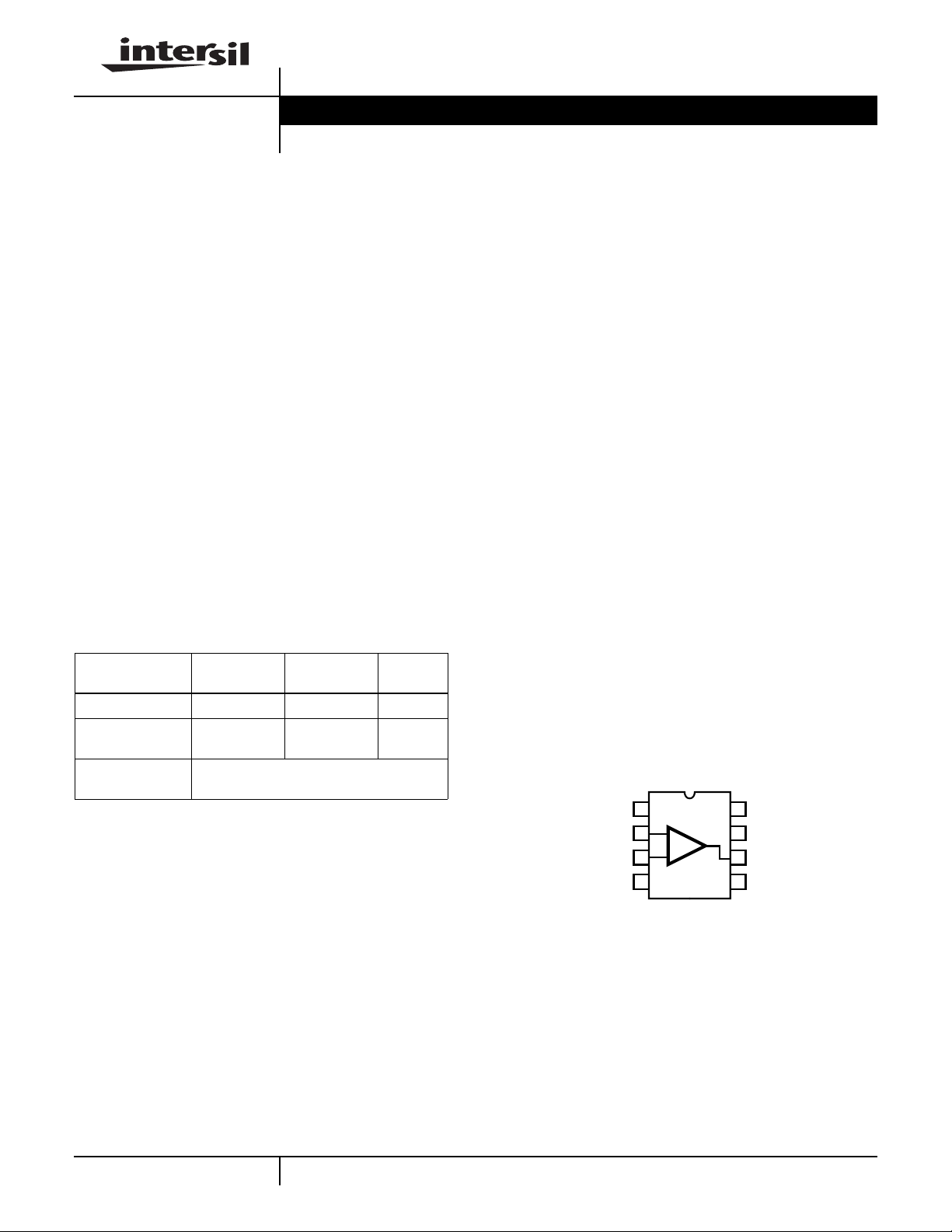
Pinout
HFA1105
(PDIP, SOIC)
TOP VIEW
NC
-IN
+IN
1
2
-
+
3
4
V-
8
NC
7
V+
6
OUT
5
NC
1
CAUTION: These devices are sensitive to electrostatic discharge; follow proper IC Handling Procedures.
http://www.intersil.com or 407-727-9207 | Copyright © Intersil Corporation 1999
Page 2
HFA1105
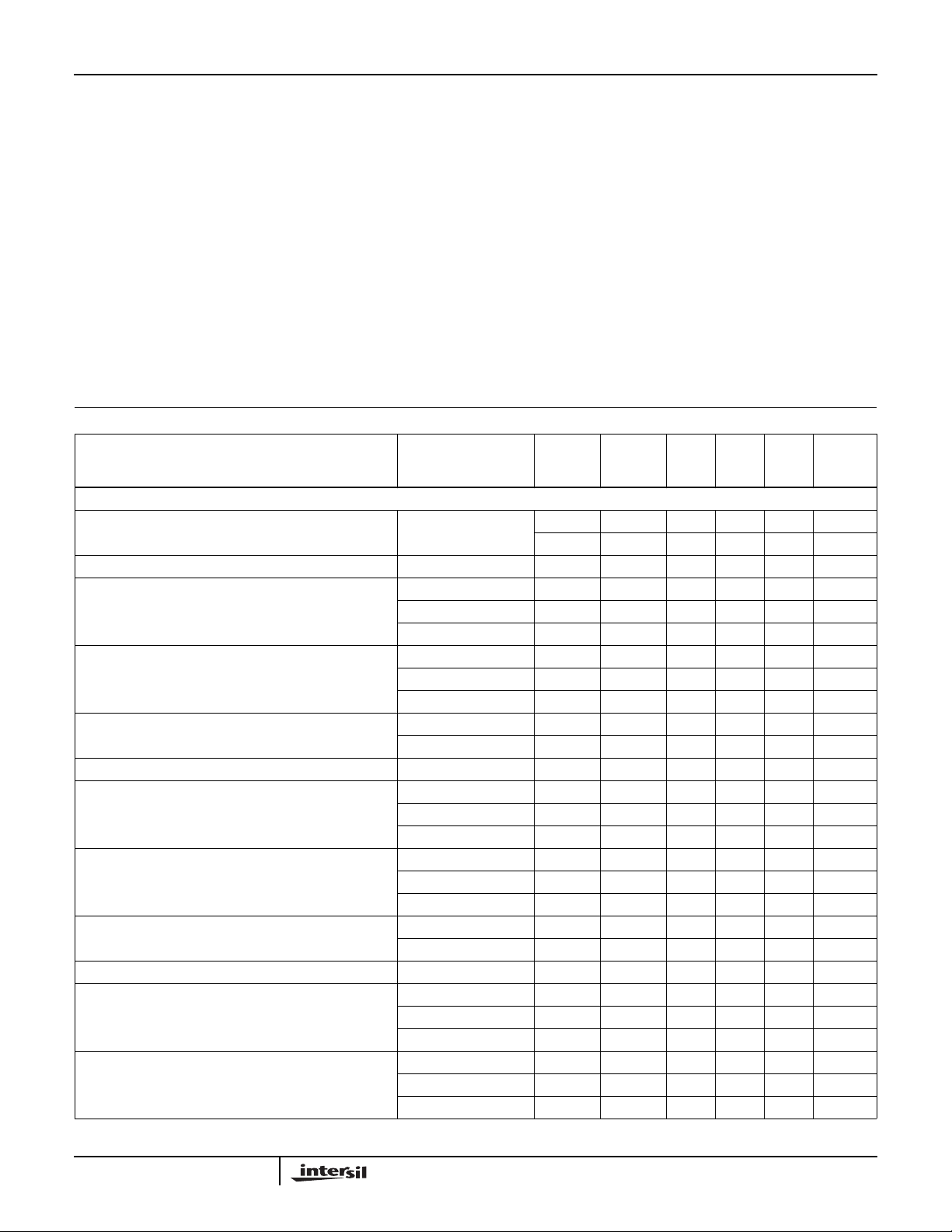
Absolute Maximum Ratings Thermal Information
Supply Voltage (V+ to V-). . . . . . . . . . . . . . . . . . . . . . . . . . . . . . 11V
DC Input Voltage . . . . . . . . . . . . . . . . . . . . . . . . . . . . . . . . V
Differential Input Voltage . . . . . . . . . . . . . . . . . . . . . . . . . . . . . . . 8V
Output Current (Note 1). . . . . . . . . . . . . . . . .Short Circuit Protected
30mA Continuous
60mA ≤ 50% Duty Cycle
ESD Rating . . . . . . . . . . . . . . . . . . . . . . . . . . . . . . . . . . . . . . >600V
SUPPLY
Operating Conditions
Temperature Range. . . . . . . . . . . . . . . . . . . . . . . . . . -40oC to 85oC
CAUTION: Stresses above those listed in “Absolute Maximum Ratings” may cause permanent damage to the device. This is a stress only rating and operationofthe
device at these or any other conditions above those indicated in the operational sections of this specification is not implied.
NOTES:
1. Output is short circuit protected to ground. Brief short circuits to ground will not degrade reliability, however continuous (100% duty cycle) output
current must not exceed 30mA for maximum reliability.
2. θJA is measured with the component mounted on an evaluation PC board in free air.
Thermal Resistance (Typical, Note 2) θJA (oC/W)
PDIP Package . . . . . . . . . . . . . . . . . . . . . . . . . . . . . 130
SOIC Package . . . . . . . . . . . . . . . . . . . . . . . . . . . . . 170
Maximum Junction Temperature (Die) . . . . . . . . . . . . . . . . . . . .175oC
Maximum Junction Temperature (Plastic Package) . . . . . . . .150oC
Maximum Storage Temperature Range. . . . . . . . . . -65oC to 150oC
Maximum Lead Temperature (Soldering 10s) . . . . . . . . . . . . 300oC
(SOIC - Lead Tips Only)
Electrical Specifications V
PARAMETER TEST CONDITIONS
INPUT CHARACTERISTICS
Input Offset Voltage A 25 - 2 5 mV
Average Input Offset Voltage Drift B Full - 1 10 µV/oC
Input Offset Voltage
Common-Mode Rejection Ratio
Input Offset Voltage
Power Supply Rejection Ratio
Non-Inverting Input Bias Current A 25 - 6 15 µA
Non-Inverting Input Bias Current Drift B Full - 5 60 nA/oC
Non-Inverting Input Bias Current
Power Supply Sensitivity
Non-Inverting Input Resistance ∆VCM = ±1.8V A 25 0.8 1.2 - MΩ
Inverting Input Bias Current A 25 - 2 7.5 µA
Inverting Input Bias Current Drift B Full - 60 200 nA/oC
Inverting Input Bias Current
Common-Mode Sensitivity
Inverting Input Bias Current
Power Supply Sensitivity
= ±5V, AV = +1, RF = 510Ω, RL = 100Ω, Unless Otherwise Specified
SUPPLY
(NOTE 3)
TEST
LEVEL
A Full - 3 8 mV
∆VCM = ±1.8V A 25 47 50 - dB
∆VCM = ±1.8V A 85 45 48 - dB
∆VCM = ±1.2V A -40 45 48 - dB
∆VPS = ±1.8V A 25 50 54 - dB
∆VPS = ±1.8V A 85 47 50 - dB
∆VPS = ±1.2V A -40 47 50 - dB
A Full - 10 25 µA
∆VPS = ±1.8V A 25 - 0.5 1 µA/V
∆VPS = ±1.8V A 85 - 0.8 3 µA/V
∆VPS = ±1.2V A -40 - 0.8 3 µA/V
∆VCM = ±1.8V A 85 0.5 0.8 - MΩ
∆VCM = ±1.2V A -40 0.5 0.8 - MΩ
A Full - 5 15 µA
∆VCM = ±1.8V A 25 - 3 6 µA/V
∆VCM = ±1.8V A 85 - 4 8 µA/V
∆VCM = ±1.2V A -40 - 4 8 µA/V
∆VPS = ±1.8V A 25 - 2 5 µA/V
∆VPS = ±1.8V A 85 - 4 8 µA/V
∆VPS = ±1.2V A -40 - 4 8 µA/V
TEMP.
(oC) MIN TYP MAX UNITS
2
Page 3
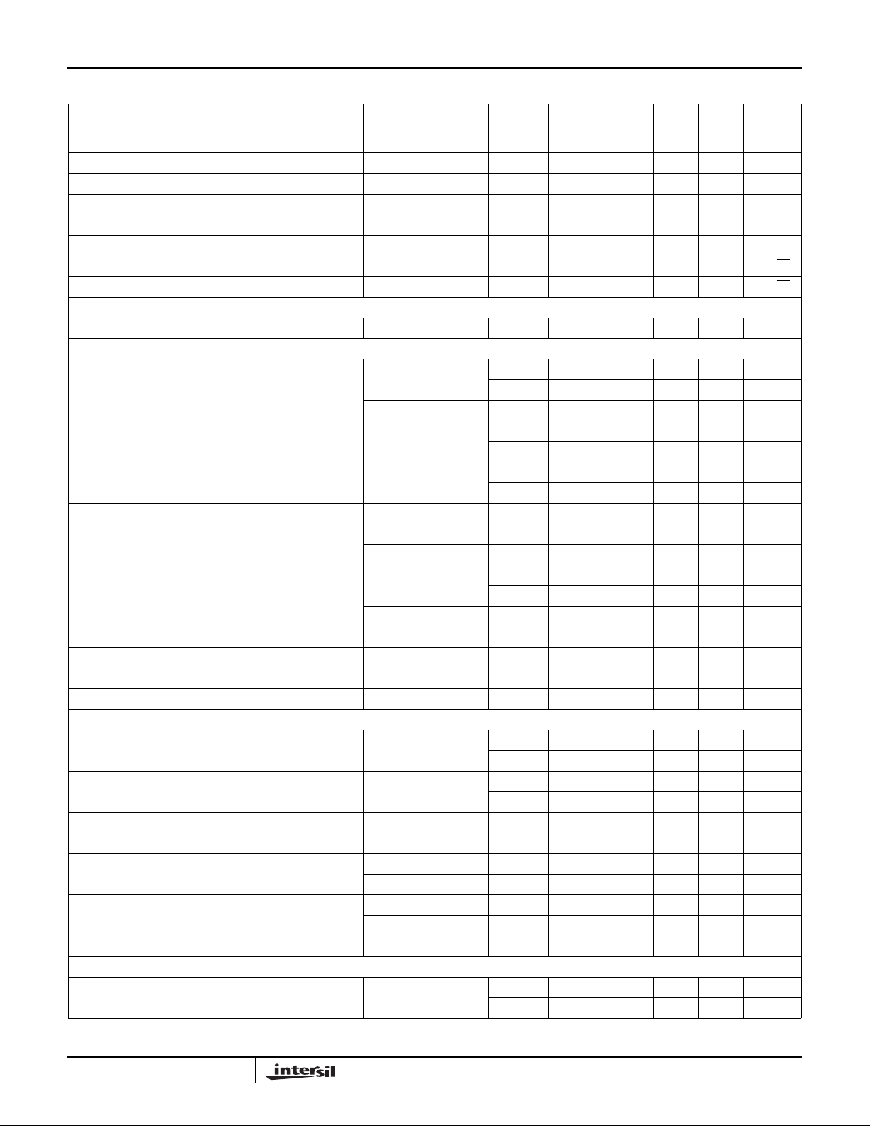
HFA1105
Electrical Specifications V
PARAMETER TEST CONDITIONS
= ±5V, AV = +1, RF = 510Ω, RL = 100Ω, Unless Otherwise Specified (Continued)
SUPPLY
(NOTE 3)
TEST
LEVEL
TEMP.
(oC) MIN TYP MAX UNITS
Inverting Input Resistance C 25 - 60 - Ω
Input Capacitance C 25 - 1.6 - pF
Input Voltage Common Mode Range
(Implied by VIO CMRR, +RIN, and -I
CMS Tests)
BIAS
A 25, 85 ±1.8 ±2.4 - V
A -40 ±1.2 ±1.7 - V
Input Noise Voltage Density (Note 6) f = 100kHz B 25 - 3.5 - nV/√Hz
Non-Inverting Input Noise Current Density (Note 6) f = 100kHz B 25 - 2.5 - pA/√Hz
Inverting Input Noise Current Density (Note 6) f = 100kHz B 25 - 20 - pA/√Hz
TRANSFER CHARACTERISTICS
Open Loop Transimpedance Gain AV = -1 C 25 - 500 - kΩ
AC CHARACTERISTICS RF = 510Ω, Unless Otherwise Specified
-3dB Bandwidth
(V
= 0.2V
OUT
P-P
, Note 6)
AV = +1, +RS = 510Ω B 25 - 270 - MHz
B Full - 240 - MHz
AV = -1, RF = 425Ω B 25 - 300 - MHz
AV = +2 B 25 - 330 - MHz
B Full - 260 - MHz
AV = +10, RF = 180Ω B 25 - 130 - MHz
B Full - 90 - MHz
Full Power Bandwidth
(V
4V
OUT
P-P
= 5V
at AV = +2/-1,
P-P
at AV = +1, Note 6)
Gain Flatness
(AV = +2, V
OUT
= 0.2V
P-P
, Note 6)
AV = +1, +RS = 510Ω B 25 - 135 - MHz
AV = -1 B 25 - 140 - MHz
AV = +2 B 25 - 115 - MHz
To 25MHz B 25 - ±0.03 - dB
B Full - ±0.04 - dB
To 75MHz B 25 - ±0.11 - dB
B Full - ±0.22 - dB
Gain Flatness
(AV = +1, +RS = 510Ω, V
OUT
= 0.2V
P-P
, Note 6)
To 25MHz B 25 - ±0.03 - dB
To 75MHz B 25 - ±0.09 - dB
Minimum Stable gain A Full - 1 - V/V
OUTPUT CHARACTERISTICS AV = +2, RF = 510Ω, Unless Otherwise Specified
Output Voltage Swing (Note 6) AV = -1, RL = 100Ω A25±3 ±3.4 - V
A Full ±2.8 ±3- V
Output Current (Note 6) AV = -1, RL = 50Ω A 25, 85 50 60 - mA
A -40 28 42 - mA
Output Short Circuit Current B 25 - 90 - mA
Closed Loop Output Impedance (Note 6) DC B 25 - 0.08 - Ω
Second Harmonic Distortion
(V
OUT
= 2V
P-P
, Note 6)
Third Harmonic Distortion
(V
OUT
= 2V
P-P
, Note 6)
10MHz B 25 - -48 - dBc
20MHz B 25 - -44 - dBc
10MHz B 25 - -50 - dBc
20MHz B 25 - -45 - dBc
Reverse Isolation (S12, Note 6) 30MHz B 25 - -55 - dB
TRANSIENT CHARACTERISTICS AV = +2, RF = 510Ω, Unless Otherwise Specified
Rise and Fall Times V
OUT
= 0.5V
P-P
B 25 - 1.1 - ns
B Full - 1.4 - ns
3
Page 4
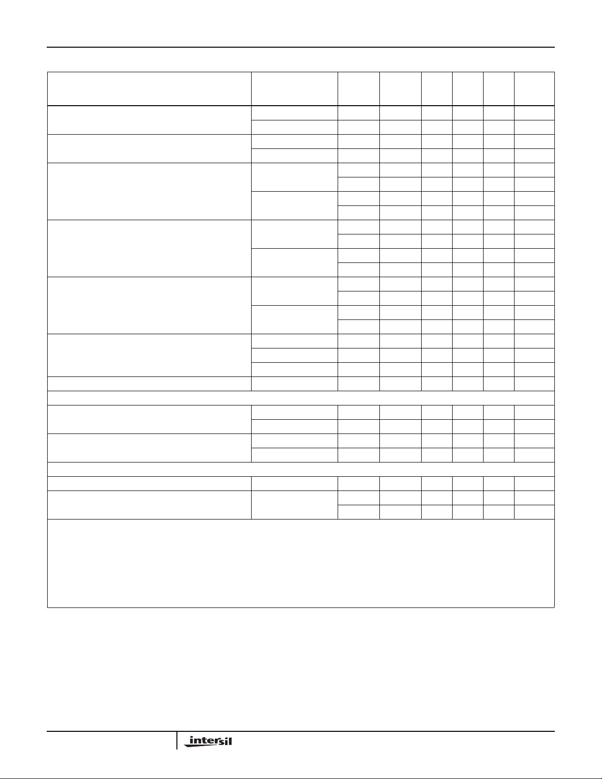
HFA1105
Electrical Specifications V
PARAMETER TEST CONDITIONS
Overshoot (Note 4)
(V
= 0 to 0.5V, VIN t
OUT
Overshoot (Note 4)
(V
= 0.5V
OUT
Slew Rate
(V
= 4V
OUT
Slew Rate
(V
= 5V
OUT
Slew Rate
(V
= 5V
OUT
Settling Time
(V
= +2V to 0V step, Note 6)
OUT
Overdrive Recovery Time VIN = ±2V B 25 - 8.5 - ns
VIDEO CHARACTERISTICS AV = +2, RF = 510Ω, Unless Otherwise Specified
Differential Gain
(f = 3.58MHz)
Differential Phase
(f = 3.58MHz)
POWER SUPPLY CHARACTERISTICS
Power Supply Range C 25 ±4.5 - ±5.5 V
Power Supply Current (Note 6) A 25 - 5.8 6.1 mA
NOTES:
3. Test Level: A. Production Tested; B. Typical or Guaranteed Limit Based on Characterization; C. Design Typical for Information Only.
4. Undershoot dominates for output signal swings below GND (e.g., 0.5V
condition. See the “Application Information” section for details.
5. Slew rates are asymmetrical if the output swings belowGND(e.g.abipolarsignal). Positive unipolar output signals have symmetric positive and
negative slew rates comparable to the +SR specification. See the “Application Information” section, and the pulse response graphs for details.
6. See Typical Performance Curves for more information.
, VIN t
P-P
, AV = +1, +RS = 510Ω)
P-P
, AV = +2)
P-P
, AV = -1)
P-P
RISE
RISE
= 1ns)
= 1ns)
= ±5V, AV = +1, RF = 510Ω, RL = 100Ω, Unless Otherwise Specified (Continued)
SUPPLY
(NOTE 3)
TEST
LEVEL
+OS B 25 - 3 - %
-OS B 25 - 5 - %
+OS B 25 - 3 - %
-OS B 25 - 11 - %
+SR B 25 - 1000 - V/µs
B Full - 975 - V/µs
-SR (Note 5) B 25 - 650 - V/µs
B Full - 580 - V/µs
+SR B 25 - 1400 - V/µs
B Full - 1200 - V/µs
-SR (Note 5) B 25 - 800 - V/µs
B Full - 700 - V/µs
+SR B 25 - 2100 - V/µs
B Full - 1900 - V/µs
-SR (Note 5) B 25 - 1000 - V/µs
B Full - 900 - V/µs
To 0.1% B 25 - 15 - ns
To 0.05% B 25 - 23 - ns
To 0.02% B 25 - 30 - ns
RL = 150Ω B 25 - 0.02 - %
RL = 75Ω B 25 - 0.03 - %
RL = 150Ω B 25 - 0.03 - Degrees
RL = 75Ω B 25 - 0.05 - Degrees
A Full - 5.9 6.3 mA
), yielding a higher overshoot limit compared to the V
P-P
TEMP.
(oC) MIN TYP MAX UNITS
OUT
= 0 to 0.5V
Application Information
Optimum Feedback Resistor
Although a current feedback amplifier’s bandwidth
dependency on closed loop gain isn’t as severe as that of a
voltage feedback amplifier, there can be an appreciable
decrease in bandwidth at higher gains. This decrease may
be minimized by taking advantage of the current feedback
4
amplifier’s unique relationship between bandwidth and R
.
F
All current feedback amplifiers require a feedback resistor,
even for unity gain applications, and R
, in conjunction with
F
the internal compensation capacitor, sets the dominant pole
of the frequency response. Thus, the amplifier’s bandwidth is
inversely proportional to R
optimized for R
= 510Ω at a gain of +2. Decreasing R
F
. The HFA1105 design is
F
F
decreases stability, resulting in excessive peaking and
Page 5

HFA1105
overshoot (Note: Capacitive feedback will cause the same
problemsdue to the feedbackimpedance decrease at higher
frequencies). At higher gains, however, the amplifier is more
stable so R
can be decreased in a trade-off of stability for
F
bandwidth.
The table below lists recommended R
values for various
F
gains, and the expected bandwidth. For a gain of +1, a
resistor (
+R
) in series with +IN is required to reduce gain
S
peaking and increase stability.
GAIN
(ACL)R
-1 425 300
+1 510 (+RS = 510Ω) 270
+2 510 330
+5 200 300
+10 180 130
(Ω)
F
BANDWIDTH
(MHz)
Non-Inverting Input Source Impedance
For best operation, the DC source impedance seen by the
non-inverting input should be ≥50Ω. This is especially
important in inverting gain configurations where the noninverting input would normally be connected directly to GND.
Pulse Undershoot and Asymmetrical Slew Rates
The HFA1105 utilizes a quasi-complementary output stage to
achievehighoutput current while minimizing quiescent supply
current. In this approach, a composite device replaces the
traditional PNP pulldown transistor. The composite device
switches modes after crossing 0V, resulting in added
distortion for signals swinging below ground, and an
increased undershoot on the negative portion of the output
waveform (See Figures 5, 8, and 11). This undershoot isn’t
present for small bipolar signals, or large positive signals.
Another artifact of the composite device is asymmetrical slew
rates for output signals with a negative voltage component.
The slew rate degrades as the output signal crosses through
0V (See Figures 5, 8, and 11), resulting in a slower overall
negative slew rate. Positive only signals have symmetrical
slew rates as illustrated in the large signal positive pulse
response graphs (See Figures 4, 7, and 10).
Terminated microstrip signal lines are recommended at the
device’s input and output connections. Capacitance,
parasitic or planned, connected to the output must be
minimized, or isolated as discussed in the next section.
Care must also be taken to minimize the capacitance to
ground at the amplifier’s inverting input (-IN), as this
capacitance causes gain peaking, pulse overshoot, and if
large enough, instability. To reduce this capacitance, the
designer should remove the ground plane under traces
connected to
-IN, and keep connections to -IN as short as possible.
An example of a good high frequency layout is the
Evaluation Board shown in Figure 2.
Driving Capacitive Loads
Capacitive loads, such as an A/D input, or an improperly
terminated transmission line will degrade the amplifier’s
phase margin resulting in frequency response peaking and
possible oscillations. In most cases, the oscillation can be
avoided by placing a resistor (R
prior to the capacitance.
Figure 1 details starting points for the selection of this
resistor. The points on the curve indicate the R
combinations for the optimum bandwidth, stability, and
settling time, but experimental fine tuning is recommended.
Picking a point above or to the right of the curve yields an
overdampedresponse,while points below or left of the curve
indicate areas of underdamped performance.
R
and CLform a low pass network at the output, thus limiting
S
system bandwidth well below the amplifier bandwidth of
270MHz (for A
= +1). By decreasing RSas CLincreases (as
V
illustrated in the curves), the maximum bandwidth is obtained
without sacrificing stability. In spite of this, the bandwidth
decreases as the load capacitance increases. For example, at
A
= +1, RS=62Ω,CL= 40pF, the overallbandwidth is limited
V
to 180MHz, and bandwidth drops to 75MHz at A
R
=8Ω, CL = 400pF.
S
) in series with the output
S
and C
S
= +1,
V
L
PC Board Layout
The amplifier’s frequency response depends greatly on the
care taken in designing the PC board. The use of low
inductance components such as chip resistors and chip
capacitors is strongly recommended, while a solid
ground plane is a must!
Attention should be given to decoupling the power supplies.
A large value (10µF) tantalum in parallel with a small value
(0.1µF) chip capacitor works well in most cases.
5
Page 6

HFA1105
50
40
30
20
10
SERIES OUTPUT RESISTANCE (Ω)
0
0 100 200 300 400
LOAD CAPACITANCE (pF)
AV = +1
AV = +2
150 250 35050
FIGURE 1. RECOMMENDED SERIES OUTPUT RESISTOR vs
LOAD CAPACITANCE
Evaluation Board
The performance of the HFA1105 may be evaluated using
the HFA11XX Evaluation Board.
The layout and schematic of the board are shown in Figure
2. To order evaluationboards (part number HFA11XXEVAL),
please contact your local sales office.
10µF
510 510
R
1
50Ω
IN
0.1µF
-5V
1
2
3
4
8
7
6
5
GND
0.1µF
50Ω
V
H
GND
OUT
V
L
10µF
+5V
FIGURE 2C. SCHEMATIC
FIGURE 2. EVALUATION BOARD SCHEMATIC AND LAYOUT
V
H
1
+IN
FIGURE 2A. TOP LAYOUT
OUT
V
L
V+
V-
GND
FIGURE 2B. BOTTOM LAYOUT
6
Page 7

HFA1105
T ypical P erf ormance Curves
200
AV = +1
+R
= 510Ω
150
100
-50
-100
OUTPUT VOLTAGE (mV)
-150
-200
2.0
1.5
1.0
S
50
0
TIME (5ns/DIV.)
FIGURE 3. SMALL SIGNAL PULSE RESPONSE FIGURE 4. LARGE SIGNAL POSITIVE PULSE RESPONSE
AV = +1
+RS = 510Ω
V
SUPPLY
= ±5V, RF = 510Ω, TA = 25oC, RL = 100Ω, Unless Otherwise Specified
3.0
AV = +1
+RS = 510Ω
2.5
2.0
1.5
1.0
0.5
0
OUTPUT VOLTAGE (V)
-0.5
-1.0
TIME (5ns/DIV.)
200
AV = +2
150
100
0.5
-0.5
-1.0
OUTPUT VOLTAGE (V)
-1.5
-2.0
0
TIME (5ns/DIV.)
50
0
-50
-100
OUTPUT VOLTAGE (mV)
-150
-200
TIME (5ns/DIV.)
FIGURE 5. LARGE SIGNAL BIPOLAR PULSE RESPONSE FIGURE 6. SMALL SIGNAL PULSE RESPONSE
3.0
2.5
2.0
1.5
1.0
0.5
OUTPUT VOLTAGE (V)
AV = +2 AV = +2
0
2.0
1.5
1.0
0.5
-0.5
OUTPUT VOLTAGE (V)
-1.0
0
-0.5
-1.0
TIME (5ns/DIV.)
-1.5
-2.0
TIME (5ns/DIV.)
FIGURE 7. LARGE SIGNAL POSITIVE PULSE RESPONSE FIGURE 8. LARGE SIGNAL BIPOLAR PULSE RESPONSE
7
Page 8

G
HFA1105
T ypical P erf ormance Curves
200
AV = +10
R
150
100
50
-50
-100
OUTPUT VOLTAGE (mV)
-150
-200
2.0
1.5
1.0
E (V)
0.5
= 180Ω
F
0
TIME (5ns/DIV.)
FIGURE 9. SMALL SIGNAL PULSE RESPONSE FIGURE 10. LARGE SIGNAL POSITIVE PULSE RESPONSE
AV = +10
R
= 180Ω
F
V
SUPPLY
= ±5V, RF = 510Ω, TA = 25oC, RL = 100Ω, Unless Otherwise Specified (Continued)
3.0
AV = +10
R
= 180Ω
F
2.5
2.0
1.5
1.0
0.5
0
OUTPUT VOLTAGE (V)
-0.5
-1.0
TIME (5ns/DIV.)
V
= 200mV
+RS = 510Ω (+1)
3
+R
0
-3
GAIN (dB)
OUT
= 0Ω (-1)
S
P-P
AV = +1
AV = -1
0
P-P
P-P
0
90
180
270
NORMALIZED PHASE (DEGREES)
0
90
180
270
PHASE (DEGREES)
V
OUT
V
OUT
AV = -1
AV = +1
= 200mV
P-P
= 5V
-0.5
-1.0
OUTPUT VOLTA
-1.5
-2.0
TIME (5ns/DIV.)
FIGURE 11. LARGE SIGNAL BIPOLAR PULSE RESPONSE
3
0
-3
NORMALIZED GAIN (dB)
V
= 200mV
OUT
RF = 510Ω (+2)
R
= 200Ω (+5)
F
R
= 180Ω (+10)
F
0.3 1 10 100 500
FIGURE 13. FREQUENCY RESPONSE FIGURE 14. FREQUENCY RESPONSE FOR VARIOUSOUTPUT
P-P
FREQUENCY (MHz)
AV = +10
AV = +5
AV = +10
AV = +5
AV = +2
AV = +2
0
90
180
270
PHASE (DEGREES)
0.3 1 10 100 500
FREQUENCY (MHz)
FIGURE 12. FREQUENCY RESPONSE
AV = +2
3
0
V
= 1.5V
-3
NORMALIZED GAIN (dB)
0.3 1 10 100 500
OUT
V
OUT
V
OUT
FREQUENCY (MHz)
= 5V
V
OUT
= 1.5V
P-P
P-P
= 200mV
P-P
VOLTAGES
8
Page 9

HFA1105
T ypical P erf ormance Curves
3
0
V
= 4V
= 5V
P-P
P-P
(+1)
(-1, +2)
FREQUENCY (MHz)
OUT
-3
V
OUT
+RS = 510Ω (+1)
NORMALIZED GAIN (dB)
1 10 100 200
V
SUPPLY
AV = +1
AV = +2
FIGURE 15. FULL POWER BANDWIDTH FIGURE 16. FREQUENCY RESPONSE FOR VARIOUS LOAD
500
400
300
200
BANDWIDTH (MHz)
100
0
-100 -50 0 50 100 150
AV = +2
= +1
A
V
= +10
A
V
TEMPERATURE (oC)
V
= 200mV
OUT
RF = 180Ω (+10)
+RS = 510Ω (+1)
= ±5V, RF = 510Ω, TA = 25oC, RL = 100Ω, Unless Otherwise Specified (Continued)
V
= 200mV
AV = -1
OUT
3
AV = +2
0
-3
NORMALIZED GAIN (dB)
0.3 1 100 500
P-P
10
FREQUENCY (MHz)
RL = 500Ω
RL = 50Ω
RL = 100Ω
RL = 1kΩ
RL = 500Ω
RL = 1kΩ
RL = 50Ω
RL = 100Ω
RESISTORS
V
= 200mV
P-P
OUT
+RS = 510Ω (+1)
0.25
0.20
0.15
0.10
0.05
0
-0.05
NORMALIZED GAIN (dB)
-0.10
11075
P-P
AV = +2
AV = +1
FREQUENCY (MHz)
0
90
180
270
PHASE (DEGREES)
FIGURE 17. -3dB BANDWIDTH vs TEMPERATURE
-40
V
= 2V
OUT
-50
-60
-70
-80
-90
REVERSE ISOLATION (dB)
0.3 1 10 100
P-P
AV = +1, +2
FREQUENCY (MHz)
FIGURE 19. REVERSE ISOLATION FIGURE 20. OUTPUT IMPEDANCE
9
AV = -1
FIGURE 18. GAIN FLATNESS
AV = +2
1K
100
10
1
0.1
0.01
OUTPUT IMPEDANCE (Ω)
0.3 1 10 100
FREQUENCY (MHz)
1000
Page 10

HFA1105
T ypical P erf ormance Curves
0.8
0.6
0.4
0.2
0.1
0
-0.2
-0.4
SETTLING ERROR (%)
-0.6
-0.8
3 8 13 18 23 28 33 38 43 48
TIME (ns)
V
SUPPLY
FIGURE 21. SETTLING RESPONSE FIGURE 22. SECOND HARMONIC DISTORTION vs P
-30
AV = +2
-40
20MHz
-50
DISTORTION (dBc)
-60
-70
-5 0 5 10 15
OUTPUT POWER (dBm)
10MHz
= ±5V, RF = 510Ω, TA = 25oC, RL = 100Ω, Unless Otherwise Specified (Continued)
-30
AV = +2
-40
10MHz
-50
20MHz
DISTORTION (dBc)
-60
-70
-5 0 5 10 15
OUTPUT POWER (dBm)
3.6
= -1
A
V
3.5
3.4
3.3
3.2
3.1
3.0
2.9
OUTPUT VOLTAGE (V)
2.8
2.7
2.6
-50 -25 0 25 50 75 100 125
+V
OUT
+V
(RL= 50Ω)
OUT
TEMPERATURE (
|-V
(RL= 100Ω)
|-V
OUT
OUT
| (RL= 100Ω)
| (RL= 50Ω)
o
C)
V
OUT
AV = +2
= 2V
OUT
FIGURE 23. THIRD HARMONIC DISTORTION vs P
100
I
NI-
10
E
NI
I
NOISE VOLTAGE (nV/√Hz)
1
0.1 1 10 100
FREQUENCY (kHz)
NI+
FIGURE 25. INPUT NOISE CHARACTERISTICS
10
OUT
100
10
1
Hz)
NOISE CURRENT (pA/√
FIGURE 24. OUTPUT VOLTAGE vs TEMPERATURE
6.1
6.0
5.9
5.8
5.7
POWER SUPPLY CURRENT (mA)
5.6
3.5 4 4.5 5 5.5 6 6.5 7 7.5
POWER SUPPLY VOLTAGE (±V)
FIGURE 26. SUPPLY CURRENT vs SUPPLY VOLTAGE
Page 11

Die Characteristics
DIE DIMENSIONS:
HFA1105
PASSIVATION:
59 mils x 59 mils x 19 mils
1500µm x 1500µm x 483µm
METALLIZATION:
Type: Metal 1: AICu(2%)/TiW
Thickness: Metal 1: 8k
Å ±0.4kÅ
Type: Metal 2: AICu(2%)
Thickness: Metal 2: 16k
Å ±0.8kÅ
Metallization Mask Layout
-IN
HFA1105
Type: Nitride
Thickness: 4k
Å ±0.5kÅ
TRANSISTOR COUNT:
75
SUBSTRATE POTENTIAL (Powered Up):
Floating
(Recommend Connection to V-)
NC
V+
OUT
+IN
V-
NC
All Intersil semiconductor products are manufactured, assembled and tested under ISO9000 quality systems certification.
Intersil semiconductor products are sold by description only. Intersil Corporation reserves the right to make changes in circuit design and/or specifications at any time without notice. Accordingly, the reader is cautioned to verify that data sheets are current before placing orders. Information furnished by Intersil is believed to be accurate and
reliable. However, no responsibility is assumed by Intersil or its subsidiaries for its use; nor for any infringements of patents or other rights of third parties which may result
from its use. No license is granted by implication or otherwise under any patent or patent rights of Intersil or its subsidiaries.
For information regarding Intersil Corporation and its products, see web site http://www.intersil.com
11
 Loading...