

Page 1

HFA1103
Data Sheet March 1999
200MHz, Video Op Amp with High Speed
Sync Stripper
The HFA1103 is a high-speed, wideband, fast settling
current feedback op amp with a sync stripping function. The
HFA1103 is a basic op amp with a modified output stage that
enables it to strip the sync from a component video signal.
The output stage has an open emitter NPN transistor that
prevents the output from going low during the sync pulse.
Removing the sync signal benefits digitizing systems
because only the active video information is applied to the
A/D converter. This enables the full dynamic range of the
A/D converter to be used to process the video signal. The
HFA1103 includes inverting input bias current adjust pins
(pins 1 and 5) for adjusting the output offset voltage.
Ordering Information
PART NUMBER
(BRAND)
HFA1103IB
(H1103I)
TEMP.
RANGE (oC) PACKAGE
-40 to 85 8 Ld SOIC M8.15
PKG.
NO.
File Number 3957.3
Features
• Removes Sync Signal From Component Video
• Low Residual Sync. . . . . . . . . . . . . . . . . . . . . . 8mV (Typ)
• -3dB Bandwidth . . . . . . . . . . . . . . . . . . . . . . . . . . 200MHz
• Very Fast Slew Rate. . . . . . . . . . . . . . . . . . . . . . . 600V/µs
• Fast Settling Time (0.1%). . . . . . . . . . . . . . . . . . . . . . 9ns
• Excellent Gain Flatness, 32MHz . . . . . . . . . . . . . . ±0.1dB
• Overdrive Recovery . . . . . . . . . . . . . . . . . . . . . . . . <12ns
Applications
• RGB Video Sync Stripping
• RGB Video Distribution Amplifier for Workstations and PC
Networks
• Video Conferencing Systems
• RGB Video Monitor Preamp
• Fiberoptic Receivers
Sync Stripper Waveforms
0 TO
+0.7V
0 TO
-0.3V
COMPONENT (RGB)
VIDEO INPUT
Application Schematic
+5V
4.7K
HFA1103
V
IN
R
IN
75
R
750
+
-
R
G
750
F
2K
R
75
L
HFA1103 OUTPUT
R
B
R
T
75
Pinout
HFA1103
1
2
3
4
(SOIC)
TOP VIEW
V+
-
+
8
NC
V+
7
OUT
6
BAL
5
0 TO
+0.7V
BAL
-IN
+IN
V-
V
OUT
R
T
75
1
CAUTION: These devices are sensitive to electrostatic discharge; follow proper IC Handling Procedures.
1-888-INTERSIL or 321-724-7143
| Copyright © Intersil Corporation 1999
Page 2
HFA1103
Absolute Maximum Ratings Thermal Information
Voltage Between V+ and V-. . . . . . . . . . . . . . . . . . . . . . . . . . . . .12V
Input Voltage . . . . . . . . . . . . . . . . . . . . . . . . . . . . . . . . . . . V
Differential Input Voltage . . . . . . . . . . . . . . . . . . . . . . . . . . . . . . . .5V
Output Current (50% Duty Cycle) . . . . . . . . . . . . . . . . . . . . . . 60mA
SUPPLY
Operating Conditions
Temperature Range. . . . . . . . . . . . . . . . . . . . . . . . . . -40oC to 85oC
CAUTION: Stresses above those listed in “Absolute Maximum Ratings” may cause permanent damage to the device. This is a stress only rating and operation of the
device at these or any other conditions above those indicated in the operational sections of this specification is not implied.
NOTE:
1. θJA is measured with the component mounted on an evaluation PC board in free air.
Thermal Resistance (Typical, Note 1) θJA (oC/W)
SOIC Package . . . . . . . . . . . . . . . . . . . . . . . . . . . . . 170
Maximum Junction Temperature (Plastic Package) . . . . . . . .150oC
Maximum Storage Temperature Range. . . . . . . . . . -65oC to 150oC
Maximum Lead Temperature (Soldering 10s) . . . . . . . . . . . . .300oC
(SOIC - Lead Tips Only)
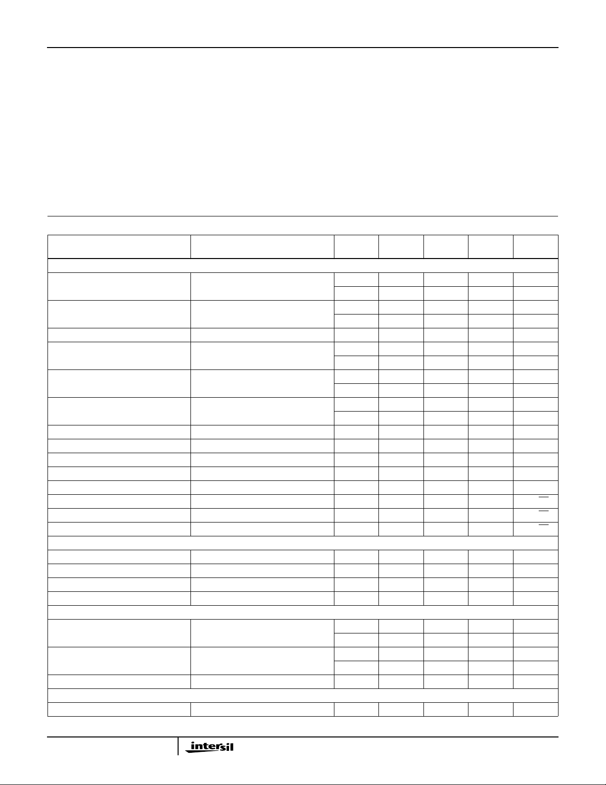
Electrical Specifications V
PARAMETER TEST CONDITIONS
DC CHARACTERISTICS
Residual Sync (Note 2) VIN = -300mV, AV = +1 25 - 8 10 mV
Output Offset Voltage (Notes 3, 5) 25 - 10 30 mV
Output Offset Voltage Drift (Note 3) Full - 10 - µV/oC
VOS PSRR ∆VS = ±1.25V 25 39 45 - dB
Non-Inverting Input Bias Current +IN = 0V 25 - 5 40 µA
Inverting Input Bias Current -IN = 0V 25 - 5 50 µA
-I
Adjust Range (Notes 4, 6) 25 100 200 - µA
BIAS
Non-Inverting Input Resistance 25 25 50 - kΩ
Inverting Input Resistance 25 - 16 30 Ω
Input Capacitance 25 - 2 - pF
Input Common Mode Range Full ±2.5 ±3.0 - V
Input Noise Voltage 100kHz 25 - 4 - nV/√Hz
+Input Noise Current 100kHz 25 - 18 - pA/√Hz
-Input Noise Current 100kHz 25 - 21 - pA/√Hz
TRANSFER CHARACTERISTICS AV = +2, Unless Otherwise Specified
Open Loop Transimpedance 25 - 500 - kΩ
-3dB Bandwidth V
Gain Flatness To ±0.1dB 25 - 32 - MHz
Minimum Stable Gain Full 1 - - V/V
OUTPUT CHARACTERISTICS AV = +2, Unless Otherwise Specified
Output Voltage (Note 3) 25, 85 2.5 3.0 - V
Output Current 25, 85 50 60 - mA
Linearity Near Zero 25 - 0.01 - %
TRANSIENT RESPONSE AV = +2, Unless Otherwise Specified
Rise Time V
= ±5V, AV = +2, RF = 750Ω, RL = 50Ω, Unless Otherwise Specified
SUPPLY
TEMP
(oC) MIN TYP MAX UNITS
Full - - 12 mV
Full - - 40 mV
Full 35 - - dB
Full - - 65 µA
Full - - 60 µA
= 1.0V
OUT
= 2.0V Step 25 - 2 - ns
OUT
, AV = +2 25 - 200 - MHz
P-P
-40oC 1.75 2.5 - V
-40oC35 50 - mA
2
Page 3

HFA1103
Electrical Specifications V
PARAMETER TEST CONDITIONS
Overshoot V
Slew Rate AV = +2, V
0.1% Settling V
Overdrive Recovery Time 2X Overdrive 25 - 12 - ns
POWER SUPPLY CHARACTERISTICS
Supply Voltage Range Full ±4.5 - ±5.5 V
Supply Current (No Load) 25 - 11 16 mA
NOTES:
2. The residual sync is specified at the output of a doubly terminated circuit (see page 1 of this data sheet).
3. Since the HFA1103 has an open emitter NPN output stage, this measurement is only valid for positive values.
4. The -I
is an open emitter NPN transistor.
5. VOS includes the error contribution of I
6. This is the minimum change in inverting input bias current when a BAL pin is connected to V- through a 50Ω resistor.
current can be used to adjust the offset voltage to zero, but -I
BIAS
Test Circuit
V
IN
R
IN
50Ω
R
750Ω
G
750Ω
= ±5V, AV = +2, RF = 750Ω, RL = 50Ω, Unless Otherwise Specified (Continued)
SUPPLY
TEMP
(oC) MIN TYP MAX UNITS
= 2.0V Step 25 - 10 - %
OUT
= 0 to 2V, +2V to 0V 25 - 600 - V/µs
OUT
= 2V to 0V 25 - 9 - ns
OUT
Full - - 23 mA
does not flow bidirectionally because the HFA1103 output stage
BIAS
at RF = 750Ω.
BSN
may cause oscillations. In most cases, the oscillation can be
DUT
+
-
V
OUT
avoided by placing a resistor in series with the output.
Care must also be taken to minimize the capacitance to
ground seen by the amplifier’sinverting input. The larger this
capacitance, the worse the gain peaking, resulting in pulse
R
F
R
50Ω
L
overshoot and possible instability. To this end, it is
recommended that the ground plane be removed under
traces connected to pin 2, and connections to pin 2 should
FIGURE 1. TEST CIRCUIT
be kept as short as possible.
Application Information
Offset Adjustment
The HFA1103allowsf oradjustmentof the inverting input bias
current to null the output offset voltage. -I
R
, so any change in bias current forces a corresponding
F
change in output voltage. The amount of adjustment is a
function of R
. With RF = 750Ω, the typical adjust range is
F
150mV. F or offset adjustment connect a 10kΩ potentiometer
between pins 1 and 5 with the wiper connected to V-.
PC Board Layout
The frequency performance of these amplifiers depends a
great deal on the amount of care taken in designing the PC
board. The use of low inductance components such as
chip resistors and chip capacitors is strongly
recommended, while a solid ground plane is a must!
Attention should be given to decoupling the power supplies.
A large value (10µF) tantalum in parallel with a small value
chip (0.1µF) capacitor works well in most cases.
Terminated microstrip signal lines are recommended at the
input and output of the device. Output capacitance, such as
that resulting from an improperly terminated transmission
line will degrade the frequency response of the amplifier and
flows through
BIAS
An example of a good high frequency layout is the
Evaluation Board shown in Figure 3.
Evaluation Board
The HFA1100 series evaluation board may be used for the
HFA1103 with minor modifications. The evaluation board
may be ordered using part number HFA11XXEVAL. Please
note that an HFA1103 sample is not included with the
evaluation board and must be ordered separately.
The layout and schematic of the board are shown below:
-5V
500Ω
1
2
3
4
8
7
6
5
GND
50Ω
V
H
10µF0.1µF
OUT
V
L
GND
500Ω
50Ω
IN
0.1µF10µF
FIGURE 2. EVALUATION BOARD SCHEMATIC
+5V
3
Page 4

HFA1103
TOP LAYOUT
V
H
1
+IN
OUT
V
L
V+
V-
GND
Typical Application
A circuit which performs the sync stripper and DC restore
functions is shown in Figure 4. Please reference Intersil
Application Note AN9514, titled “Video Amplifier with Sync
Stripper and DC Restore”, for details on this circuit.
TO SYNC
SEPARATOR
S/H
CONTROL
IC1a
+
R
1
1K
V
IN
OPT.
-
IC2
C
0.1µF
1
R
10K
R
1K
+5V
R
3
10K
2
-5V
IC1b
+
-
4
R
5
1K
BOTTOM LAYOUT
FIGURE 3. EVALUATION BOARD ARTWORK
The standard output of a VM700 video measurement set is
shown in Figure 5. The output, after passing through the
Applications Schematic shown on the first page of this data
sheet, is shown in Figure 6.
IC1a + IC1b = CA5260 DUAL AMP
IC2 = 74HC4053 SWITCH
IC3 = HFA1103 VIDEO OP AMP
R
7
750
R
6
750
C
2
47µF
IC3
-
+
R
9
10K
R
11
75
R
10
75
R
6.8K
8
+5V
R
75
DC
V
OUT
12
FIGURE 4. VIDEO AMPLIFIER WITH SYNC STRIPPER AND DC RESTORE
VOLTS IRE:FLT
100.0
0.6
0.4
0.2
0.0
-0.2
-40.0 -30.0 -20.0 -10.0 0.0 10.0
525 LINE NTSC MICROSECONDS
50.0
0.0
-50.0
FIGURE 5. OUTPUT OF VM700 VIDEO MEASUREMENT SET
4
Page 5

HFA1103
VOLTS
IRE:FLT
100.0
0.6
0.4
0.2
0.0
-0.2
-40.0 -30.0 -20.0 -10.0 0.0 10.0
525 LINE NTSC MICROSECONDS
50.0
0.0
-50.0
FIGURE 6. OUTPUT OF HFA1103 SYNC STRIPPER CONFIGURED AS ON THE FIRST PAGE OF THIS DATA SHEET
5
Page 6

Die Characteristics
HFA1103
DIE DIMENSIONS:
63 mils x 44 mils x 19 mils
1600µm x 1130µm x 483µm
METALLIZATION:
Type: Metal 1: AlCu (2%)/TiW
Thickness: Metal1: 8k
Å ±0.4kÅ
Type: Metal 2: AlCu (2%)
Thickness: 16k
Å ±0.8kÅ
Metallization Mask Layout
-IN
SUBSTRATE POTENTIAL (POWERED UP):
Floating (Recommend Connection to V-)
PASSIVATION:
Type: Nitride
Thickness: 4k
TRANSISTOR COUNT:
50
HFA1103
BAL NC
Å ±0.5kÅ
V+
+IN
V-
BALNC
OUT
All Intersil semiconductor products are manufactured, assembled and tested under ISO9000 quality systems certification.
Intersil semiconductor products aresold by description only.Intersil Corporation reserves the right to make changesin circuit design and/or specifications at anytimewithout notice. Accordingly, the reader is cautioned to verify that data sheets are current before placing orders. Information furnished by Intersil is believ edtobe accurate and
reliable. Howe ver, no responsibility is assumed by Intersil or itssubsidiaries for its use;nor for any infringements of patents or other rights of third parties which may result
from its use. No license is granted by implication or otherwise under any patent or patent rights of Intersil or its subsidiaries.
For information regarding Intersil Corporation and its products, see web site www.intersil.com
Sales Office Headquarters
NORTH AMERICA
Intersil Corporation
P. O. Box 883, Mail Stop 53-204
Melbourne, FL 32902
TEL: (321) 724-7000
FAX: (321) 724-7240
EUROPE
Intersil SA
Mercure Center
100, Rue de la Fusee
1130 Brussels, Belgium
TEL: (32) 2.724.2111
FAX: (32) 2.724.22.05
ASIA
Intersil (Taiwan) Ltd.
7F-6, No. 101 Fu Hsing North Road
Taipei, Taiwan
Republic of China
TEL: (886) 2 2716 9310
FAX: (886) 2 2715 3029
6
Page 7

Small Outline Plastic Packages (SOIC)
HFA1103
N
INDEX
AREA
123
-A-
E
-B-
SEATING PLANE
D
A
-C-
0.25(0.010) BM M
H
L
h x 45
o
α
e
B
0.25(0.010) C AM BS
M
NOTES:
1. Symbols are defined in the “MO Series Symbol List” in Section 2.2 of
Publication Number 95.
2. Dimensioning and tolerancing per ANSI Y14.5M-1982.
3. Dimension“D” does not include mold flash, protrusions or gate burrs.
Mold flash, protrusion and gate burrs shall not exceed 0.15mm (0.006
inch) per side.
4. Dimension “E” does not include interlead flash or protrusions. Interlead flash and protrusions shall not exceed 0.25mm (0.010 inch) per
side.
5. Thechamfer on the body is optional. If it is not present, a visual index
feature must be located within the crosshatched area.
6. “L” is the length of terminal for soldering to a substrate.
7. “N” is the number of terminal positions.
8. Terminal numbers are shown for reference only.
9. The lead width “B”, as measured 0.36mm (0.014 inch) or greater
above the seating plane, shall not exceed a maximum value of
0.61mm (0.024 inch).
10. Controllingdimension: MILLIMETER. Converted inch dimensions
are not necessarily exact.
A1
C
0.10(0.004)
M8.15 (JEDEC MS-012-AA ISSUE C)
8 LEAD NARROW BODY SMALL OUTLINE PLASTIC
PACKAGE
INCHES MILLIMETERS
SYMBOL
A 0.0532 0.0688 1.35 1.75 -
A1 0.0040 0.0098 0.10 0.25 -
B 0.013 0.020 0.33 0.51 9
C 0.0075 0.0098 0.19 0.25 D 0.1890 0.1968 4.80 5.00 3
E 0.1497 0.1574 3.80 4.00 4
e 0.050 BSC 1.27 BSC H 0.2284 0.2440 5.80 6.20 h 0.0099 0.0196 0.25 0.50 5
L 0.016 0.050 0.40 1.27 6
N8 87
o
α
0
o
8
o
0
o
8
Rev. 0 12/93
NOTESMIN MAX MIN MAX
-
All Intersil semiconductor products are manufactured, assembled and tested under ISO9000 quality systems certification.
Intersil semiconductor products are sold by description only.Intersil Corporation reserves the right to make changes in circuit design and/or specifications at any time without notice. Accordingly, the reader is cautioned to verify that data sheets are current before placing orders. Information furnished by Intersil is believed to be accurate and
reliable. However,no responsibility is assumed by Intersil or its subsidiaries for its use; nor for any infringements of patents or other rights of third parties which may result
from its use. No license is granted by implication or otherwise under any patent or patent rights of Intersil or its subsidiaries.
For information regarding Intersil Corporation and its products, see web site www.intersil.com
Sales Office Headquarters
NORTH AMERICA
Intersil Corporation
P. O. Box 883, Mail Stop 53-204
Melbourne, FL 32902
TEL: (321) 724-7000
FAX: (321) 724-7240
7
EUROPE
Intersil SA
Mercure Center
100, Rue de la Fusee
1130 Brussels, Belgium
TEL: (32) 2.724.2111
FAX: (32) 2.724.22.05
ASIA
Intersil (Taiwan) Ltd.
7F-6, No. 101 Fu Hsing North Road
Taipei, Taiwan
Republic of China
TEL: (886) 2 2716 9310
FAX: (886) 2 2715 3029
 Loading...