

Page 1
Ultrafast, Soft Recovery Diode
Bulletin PD-20618 07/00
HFA08SD60S
Features
• Ultrafast Recovery Time
• Ultrasoft Recovery
• Very Low I
• Very Low Q
• Guaranteed Avalanche
• Specified at Operating Temperature
RRM
rr
Benefits
• Reduced RFI and EMI
• Reduced Power Loss in Diode and
Switching Transistor
• Higher Frequency Operation
• Reduced Snubbing
• Reduced Parts Count
Description/ Applications
These diodes are optimized to reduce losses and EMI/RFI in
high frequency power conditioning systems. The softness of the
recovery eliminates the need for a snubber in most applications.
These devices are ideally suited for freewheeling, flyback,
power converters, motor drives, and other applications where
high speed and reduced switching losses are design
requirements.
Package Outline
I
F(AV)
D - PAK
t
= 18ns
rr
= 8Amp
VR = 600V
Absolute Maximum Ratings
Parameters Max Units
V
RRM
I
F(AV)
I
FSM
I
FRM
P
D
TJ, T
Cathode-to-Anode Voltage 600 V
Continuous Forward Current 8 A
TC = 100°C
Single Pulse Forward Current 60
Peak Repetitive Forward Current 24
Maximum Power Dissipation 14 W
TC = 100°C
Operating Junction and Storage Temperatures - 55 to 150 °C
STG
1
Page 2
HFA08SD60S
Bulletin PD-20618 07/00
Electrical Characteristics @ T
Parameters Min Typ
VBR, VrBreakdown Voltage, 600 - - V IR = 100µA
Blocking Voltage
V
F
I
R
C
T
L
S
Forward Voltage - 1.4 1.7 V IF = 8A
See Fig. 1 - 1.7 2.1 V IF = 16A
Max. Reverse Leakage Current - 0.3 5.0 µA VR = VR Rated
Junction Capacitance - 10 25 pF VR = 200V
Series Inductance - 8.0 - nH Measured lead to lead 5mm from package body
= 25°C (unless otherwise specified)
J
Max Units
- 1.4 1.7 V IF = 8A, TJ = 125°C
- 100 500 µA TJ = 125°C, VR = 0.8 x VR Rated
Test Conditions
Dynamic Recovery Characteristics @ TJ = 25°C (unless otherwise specified)
Parameters Min Typ
di
t
rr
I
RRM
Q
(rec)
rr
Reverse Recovery Time -18-nsIF = 1.0A, diF/dt = 200A/µA, VR = 30V
-3755 TJ = 25°C
-5590 TJ = 125°C
Peak Recovery Current - 3.5 5.0 A TJ = 25°C
- 4.5 8.0 TJ = 125°C
Reverse Recovery Charge - 65 138 nC TJ = 25°C
- 124 360 TJ = 125°C
/dt Rate of Fall of recovery Current - 240 - A/µs TJ = 25°C
M
- 210 - TJ = 125°C
Max
Units Test Conditions
IF = 8A
VR = 200V
diF /dt = 200A/µs
Thermal - Mechanical Characteristics
Parameters Min Typ Max Units
T
J
T
Stg
T
lead
R
thJC
R
thJA
Wt Weight - 2.0 - g
! Typical Socket Mount
2
Max. Junction Temperature Range - - - 55 to 150 °C
Max. Storage Temperature Range - - - 55 to 150
Lead Temperature - - 300
Thermal Resistance, Junction to Case - - 3.5 °C/ W
!
Thermal Resistance, Junction to Ambient - - 80
- 0.07 - (oz)
Page 3
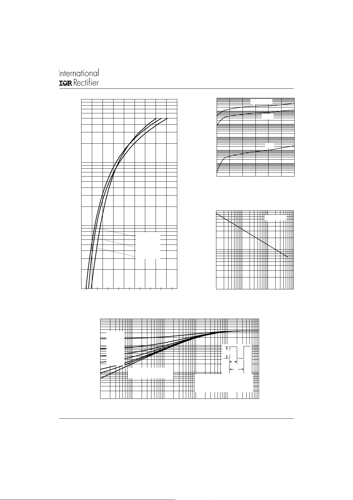
(A)
0.001
0.01
0.1
1
10
100
1000
0 100 200 300 400 500 600
125˚C
25˚C
T = 150˚C
J
0.1
1
10
00
0.4 0.8 1.2 1.6 2 2.4 2.8 3.2 3.6 4
T = 150˚C
T = 125˚C
T = 25˚C
J
J
J
Instantaneous Forward Current - I
HFA08SD60S
Bulletin PD-20618 07/00
(µA)
R
Reverse Current - I
F
Reverse Voltage - VR (V)
Fig. 2 - Typical Values Of Reverse Current
100
(pF)
T
Vs. Reverse Voltage
T = 25˚C
J
10
Junction Capacitance - C
1
1 10 100 1000
Forward Voltage Drop - V
Fig. 1 - Typical Forward Voltage Drop Characteristics
FM
(V)
Reverse Voltage - V R (V)
Fig. 3 - Typical Junction Capacitance
Vs. Reverse Voltage
10
(°C/W)
thJC
Thermal Impedance Z
D = 0.50
D = 0.20
D = 0.10
0.1
1
D = 0.05
D = 0.02
D = 0.01
Single Pulse
(Thermal Resistance)
Notes:
P
DM
t
1
t
2
1. Duty factor D = t1/ t2
2. Peak Tj = Pdm x ZthJC + Tc
.01
0.00001 0.0001 0.001 0.01 0.1 1
t1, Rectangular Pulse Duration (Seconds)
Fig. 4 - Max. Thermal Impedance Z
Characteristics
thJC
3
Page 4

HFA08SD60S
Bulletin PD-20618 07/00
80
70
60
50
trr (nC)
40
30
Vr = 200V
20
Tj = 125˚C
Tj = 25˚C
10
100 1000
di
/dt (A/ µs)
F
Fig. 5 - Typical Reverse Recovery vs. di
10000
Vr = 200V
Tj = 125˚C
Tj = 25˚C
If = 16A
If = 8A
If = 4A
20
15
If = 16A
If = 8A
If = 4A
10
Irr (A)
5
Vr = 200V
Tj = 125˚C
Tj = 25˚C
0
100 1000
Average Forward Current - I
/dt
F
Fig. 6 - Typical Recovery Current vs. di F /dt
F(AV)
(A)
10000
Vr = 200V
Tj = 125˚C
Tj = 25˚C
4
If = 16A
If = 8A
If = 4A
1000
Qrr ( nC )
100
100 1000
di F /dt (A/µs )
Fig. 7 - Typical Stored Charge vs. di
If = 16A
If = 8A
If = 4A
1000
/ dt (A/ µs)
(rec)M
di
100
100 1000
di F /dt (A/µs )
/dt
F
Fig. 8 - Typical di
(rec)M
/dt vs. di
/dt
F
Page 5

Reverse Recovery Circuit
V = 200V
R
0.01
Ω
L = 70µH
D.U.T.
HFA08SD60S
Bulletin PD-20618 07/00
di F /dt
dif/dt
ADJUST
G
Fig. 9- Reverse Recovery Parameter Test Circuit
I
F
t
a
0
1
di F /dt
di /dt
f
1. diF/dt - Rate of change of current through zero
crossing
2. I
- Peak reverse recovery current
RRM
3. t
- Reverse recovery time measured from zero
rr
crossing point of negative going IF to point where
a line passing through 0.75 I
extrapolated to zero current
RRM
and 0.50 I
RRM
3
2
D
IRFP250
S
t
rr
t
b
Q
I
RRM
0.5
di(rec)M/dt
0.75
I
RRM
4. Qrr - Area under curve defined by t
and I
RRM
Q
rr
5. di
/dt - Peak rate of change of
(rec)M
current during tb portion of t
rr
I
=
4
RRM
t rr x I
RRM
2
5
rr
rr
Fig. 10 - Reverse Recovery Waveform and Definitions
5
Page 6

HFA08SD60S
e
Bulletin PD-20618 07/00
Outline Table
6.73 (0.26)
6.35 (0.25)
5.46 (0.21)
5.21 (0.20)
4
1.64 (0.02)
123
1.52 (0.06)
1.15 (0.04)
1.14 (0.04)
2x
0.76 (0.03)
2.28 (0.09)
2x
Conform to JEDEC outline D-Pak
Dimensions in millimeters and (inches)
Tape & Reel Information
TRR
FEED DIRECTION
TRL
FEED DIRECTION
1.85 (0.073)
1.65 (0.065)
1.27 (0.05)
0.88 (0.03)
6.22 (0.24)
5.97 (0.23)
0.89 (0.03)
3x
0.64 (0.02)
4.57 (0.18)
4.10 (0.161)
3.90 (0.153)
10.9 0 (0.4 29)
10.7 0 (0.4 21)
2.38 (0.09)
2.19 (0.08)
10.42 (0.41)
9.40 (0.37)
1 - Anode
2 - Cathode
3 - Anode
4 - Cathode
1.60 (0.063)
1.50 (0.059)
1.60 (0. 063)
1.50 (0. 059)
11.6 0 (0.4 57)
11.4 0 (0.4 49)
1.75 (0.069)
1.25 (0.049)
16.1 0 (0.6 34)
15.9 0 (0.6 26)
1.14 (0.04)
0.89 (0.03)
0.58 (0.02)
0.46 (0.02)
6.45 (0.24)
5.68 (0.22)
0.51 (0.02)
MIN.
0.58 (0.02)
0.46 (0.02)
DIA.
DIA.
15.42 (0.6 09)
15.22 (0.6 01)
MINIMUM RECOMMENDED FOOTPRINT
5.97 (0.24)
6.48 (0.26)
10.67 (0.42)
2x
2.54 (0.10)
1.65 (0.06)
2x
0.368 (0.0145)
0.342 (0.0135)
24.3 0 (0.95 7)
23.9 0 (0.94 1)
4.72 (0.186)
4.52 (0.178)
2.28 (0.09)
2x
base
cathode
13
cathode
anode anod
4
2
360 (14.173)
DIA. M AX.
13.5 0 (0.5 32)
12.8 0 (0.5 04)
DIA.
26.4 0 (1.0 39)
24.4 0 (0.9 61)
60 (2 .362)
DIA. MIN.
SMD-220 Tape & Reel
When order ing, indicate th e part
SMD-220 Tape & Reel
number, part orientation, and th e
quantity. Quantities are in multiples
When ordering, indicate the part
of 8 00 pi eces p er reel for bo th
number, part orientation and the
TRL an d TRR.
quantity. Quantities are in
multiples of 800 pieces per reel for
both TRL and TRR.
6
Page 7

Marking Information
HFA08SD60S
Bulletin PD-20618 07/00
EXAMPLE: THIS IS AN HFA08SD60S
Ordering Information Table
Device Code
HF A 08 SD 60 S
1
2
1 - Hexfred Family
2 - Electron Irradiated
3 - Current Rating (08 = 8A)
4 - D-PAK
5 - Voltage Rating (60 = 600V)
6 - Suffix
INTERNATIONAL
RECTIFIER LOGO
4
3
ASSEMBLY
LOT CODE
5
2 (K)
PART NUMBER
HFA08SD60S
9812
5K3A
DATE CODE (YYWW)
YY = YEAR
1 (K) 3 (A)
WW = WEEK
6
S= D2PAK/ Dpak
TR = Tape & Reel
TRL = Tape & Reel Left
TRR = Tape & Reel Right
WORLD HEADQUARTERS: 233 Kansas St., El Segundo, California 90245 U.S.A. Tel: (310) 322 3331. Fax: (310) 322 3332.
EUROPEAN HEADQUARTERS: Hurst Green, Oxted, Surrey RH8 9BB, U.K. Tel: ++ 44 1883 732020. Fax: ++ 44 1883 733408.
IR SOUTHEAST ASIA: 1 Kim Seng Promenade, Great World City West Tower,13-11, Singapore 237994. Tel: ++ 65 838 4630.
IR CANADA: 15 Lincoln Court, Brampton, Markham, Ontario L6T3Z2. Tel: (905) 453 2200. Fax: (905) 475 8801.
IR GERMANY: Saalburgstrasse 157, 61350 Bad Homburg. Tel: ++ 49 6172 96590. Fax: ++ 49 6172 965933.
IR ITALY: Via Liguria 49, 10071 Borgaro, Torino. Tel: ++ 39 11 4510111. Fax: ++ 39 11 4510220.
IR FAR EAST: K&H Bldg., 2F, 30-4 Nishi-Ikebukuro 3-Chome, Toshima-Ku, Tokyo, Japan 171. Tel: 81 3 3983 0086.
IR TAIWAN: 16 Fl. Suite D.207, Sec. 2, Tun Haw South Road, Taipei, 10673, Taiwan. Tel: 886 2 2377 9936.
7
 Loading...