

Page 1
INTEGRATED CIRCUITS
DATA SH EET
For a complete data sheet, please also download:
•The IC04 LOCMOS HE4000B Logic
Family Specifications HEF, HEC
•The IC04 LOCMOS HE4000B Logic
Package Outlines/Information HEF, HEC
HEF4521B
MSI
24-stage frequency divider and
oscillator
Product specification
File under Integrated Circuits, IC04
January 1995
Page 2
Philips Semiconductors Product specification
24-stage frequency divider and oscillator
DESCRIPTION
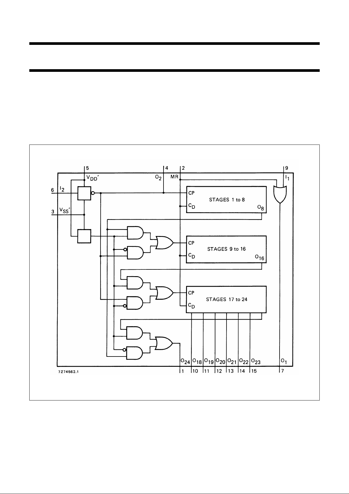
The HEF4521B consists of a chain of 24 toggle flip-flops
with an overriding asynchronous master reset input (MR),
and an input circuit that allows three modes of operation.
The single inverting stage (I2/O2) will function as a crystal
oscillator, or in combination with I1as an RC oscillator, or
as an input buffer for an external oscillator. Low-power
operation as a crystal oscillator is enabled by connecting
external resistors to pins 3 (V
Each flip-flop divides the frequency of the previous flip-flop
by two, consequently the HEF4521B will count up to
224= 16777216. The counting advances on the HIGH to
LOW transition of the clock (I2). The outputs of the last
seven stages are available for additional flexibility.
HEF4521B
’) and 5 (VDD’).
SS
MSI
Fig.1 Functional diagram.
FAMILY DATA, I
See Family Specifications
January 1995 2
LIMITS category MSI
DD
Page 3
Philips Semiconductors Product specification
24-stage frequency divider and oscillator
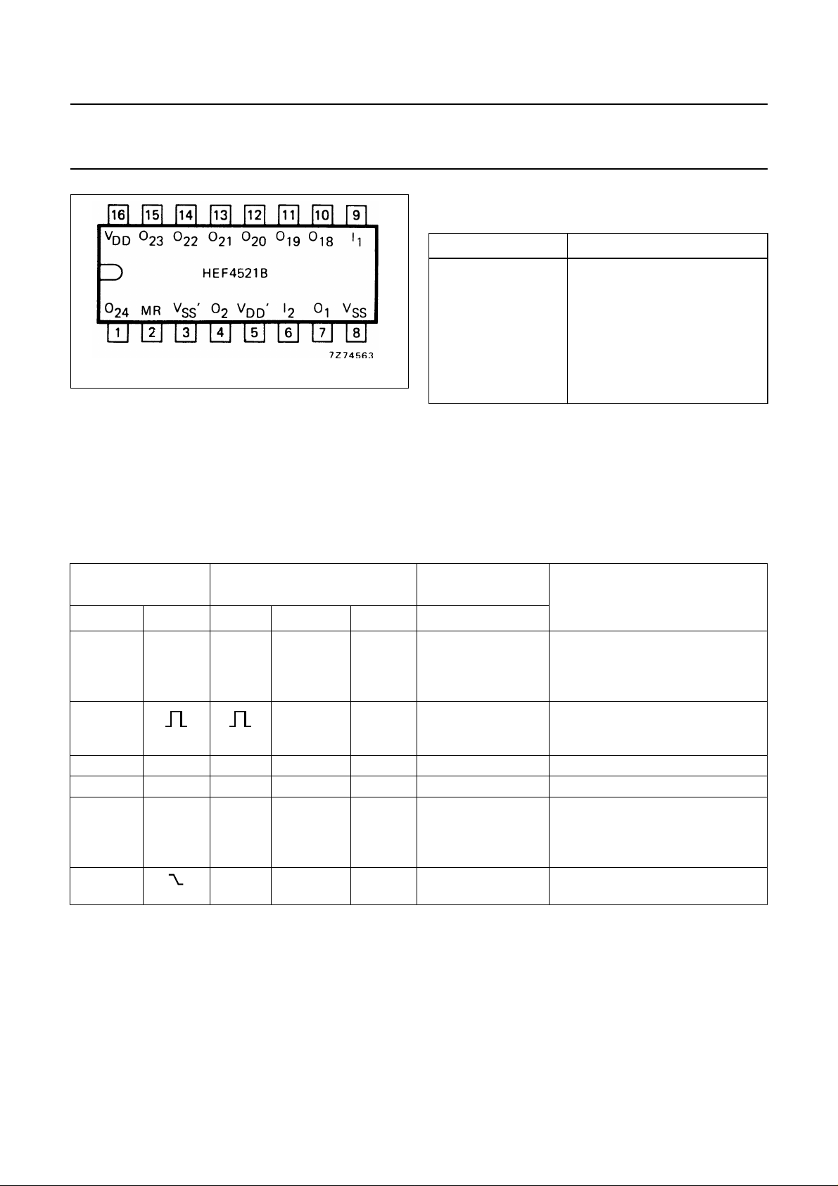
Fig.2 Pinning diagram.
HEF4521BP(N): 16-lead DIL; plastic (SOT38-1)
HEF4521BD(F): 16-lead DIL; ceramic (cerdip) (SOT74)
HEF4521BT(D): 16-lead SO; plastic (SOT109-1)
( ): Package Designator North America
COUNT CAPACITY
OUTPUT COUNT CAPACITY
O
18
O
19
O
20
O
21
O
22
O
23
O
24
218= 262 144
219= 524 288
220= 1 048 576
221= 2 097 152
222= 4 194 304
223= 8 388 608
224= 16 777 216
HEF4521B
MSI
FUNCTIONAL TEST SEQUENCE
INPUTS
MR I
2
O
HLLVDDV
LV
LLLV
LHLVSSV
LHLV
LV
TERMINALS
2
CONTROL
VSS’V
DD
SS
SS
SS
DD
V
V
V
V
’O
SS
SS
SS
SS
DD
DD
A test function has been included for the reduction of the
test time required to exercise all 24 counter stages. This
test function divides the counter into three 8-stage
sections by connecting VSS’toVDDand VDD’toVSS. Via
I2(connected to O2) 255 counts are loaded into each of
the 8-stage sections in parallel. All flip-flops are now at a
HIGH state.
OUTPUTS
REMARKS
to O
18
24
L counter is in three 8-stage sections
in parallel mode; I2and O2are
interconnected (O2is now input);
counter is reset by MR
H 255 pulses are clocked into I2,O
2
(the counter advances on the LOW
to HIGH transition)
HV
’ is connected to V
SS
SS
H the input I2is made HIGH
HV
’ is connected to VDD;O2is
DD
now made floating and becomes an
output; the device is now in the
224mode
L
counter ripples from an all HIGH
state to an all LOW state
The counter is now returned to the normal 24-stage in
series configuration by connecting VSS’ to VSSand VDD’to
VDD. One more pulse is entered into input I2, which will
cause the counter to ripple from an all HIGH state to an all
LOW state.
January 1995 3
Page 4
This text is here in white to force landscape pages to be rotated correctly when browsing through the pdf in the Acrobat reader.This text is here in
_white to force landscape pages to be rotated correctly when browsing through the pdf in the Acrobat reader.This text is here inThis text is here in
white to force landscape pages to be rotated correctly when browsing through the pdf in the Acrobat reader. white to force landscape pages to be ...
January 1995 4
Philips Semiconductors Product specification
24-stage frequency divider and oscillator
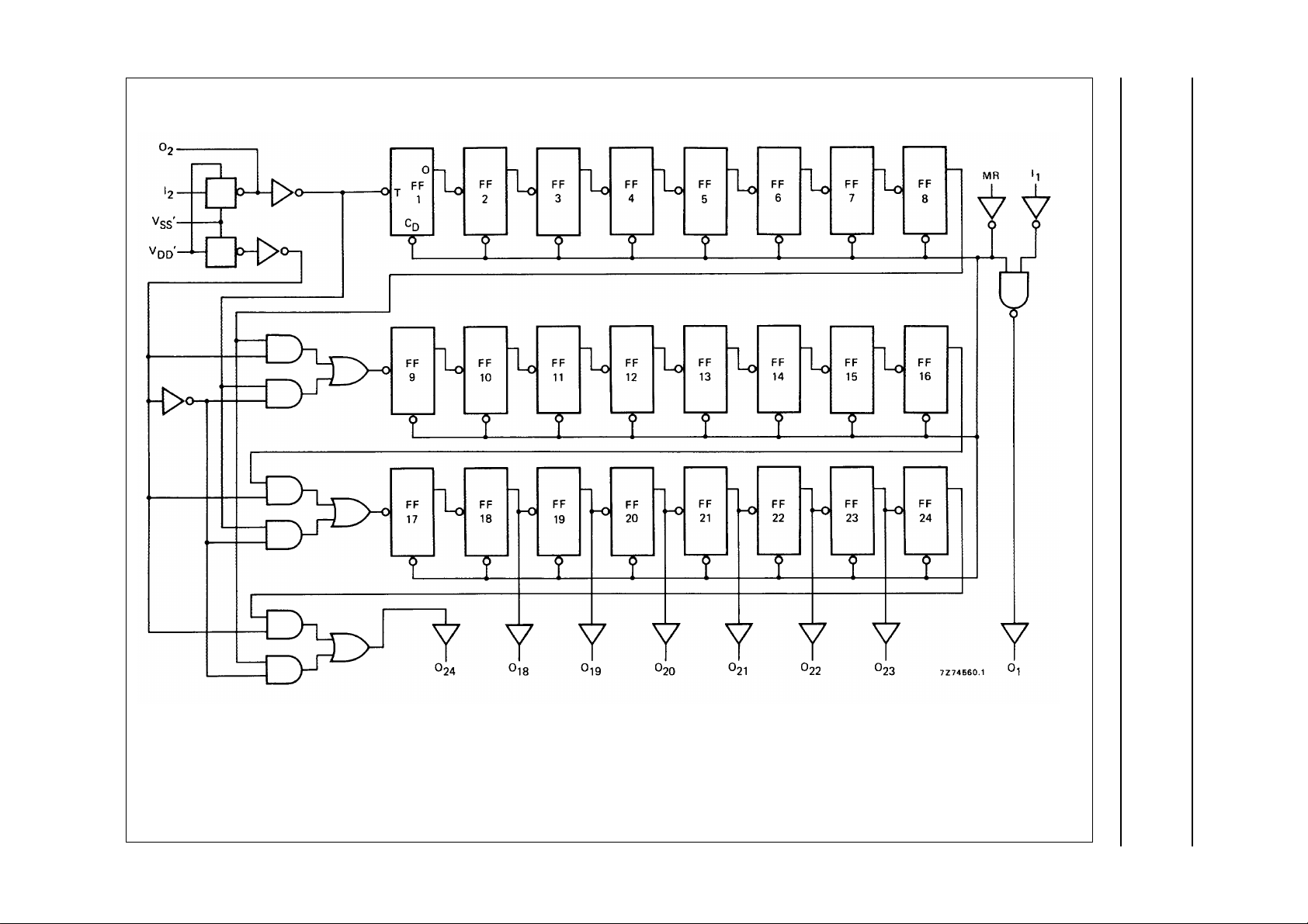
Fig.3 Logic diagram; for schematic diagram of clock circuit see Fig.4.
HEF4521B
MSI
Page 5
Philips Semiconductors Product specification
24-stage frequency divider and oscillator
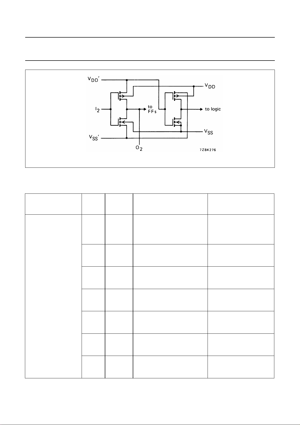
Fig.4 Schematic diagram of clock input circuitry.
AC CHARACTERISTICS
V
= 0 V; T
SS
=25°C; CL= 50 pF; input transition times ≤ 20 ns
amb
HEF4521B
MSI
V
DD
V SYMBOL MIN. TYP. MAX.
TYPICAL
EXTRAPOLATION
FORMULA
Propagation delays
I2→ O
18
HIGH to LOW 10 t
5 950 1900 ns 923 ns + (0,55 ns/pF) C
PHL
350 700 ns 339 ns + (0,23 ns/pF) C
15 220 440 ns 212 ns + (0,16 ns/pF) C
5 950 1900 ns 923 ns + (0,55 ns/pF) C
LOW to HIGH 10 t
PLH
350 700 ns 339 ns + (0,23 ns/pF) C
15 220 440 ns 212 ns + (0,16 ns/pF) C
On→ On+ 1 5 40 80 ns 13 ns + (0,55 ns/pF) C
HIGH to LOW 10 t
PHL
15 30 ns 4 ns + (0,23 ns/pF) C
15 10 20 ns 2 ns + (0,16 ns/pF) C
5 40 80 ns 13 ns + (0,55 ns/pF) C
LOW to HIGH 10 t
PLH
15 30 ns 4 ns + (0,23 ns/pF) C
15 10 20 ns 2 ns + (0,16 ns/pF) C
MR → O
n
HIGH to LOW 10 t
5 120 240 ns 93 ns + (0,55 ns/pF) C
PHL
55 110 ns 44 ns + (0,23 ns/pF) C
15 40 80 ns 32 ns + (0,16 ns/pF) C
I1→ O
1
HIGH to LOW 10 t
5 90 180 ns 63 ns + (0,55 ns/pF) C
PHL
35 70 ns 24 ns + (0,23 ns/pF) C
15 25 50 ns 17 ns + (0,16 ns/pF) C
5 60 120 ns 33 ns + (0,55 ns/pF) C
LOW to HIGH 10 t
PLH
30 60 ns 19 ns + (0,23 ns/pF) C
15 20 40 ns 12 ns + (0,16 ns/pF) C
L
L
L
L
L
L
L
L
L
L
L
L
L
L
L
L
L
L
L
L
L
January 1995 5
Page 6
Philips Semiconductors Product specification
24-stage frequency divider and oscillator
HEF4521B
MSI
V
DD
V SYMBOL MIN. TYP. MAX.
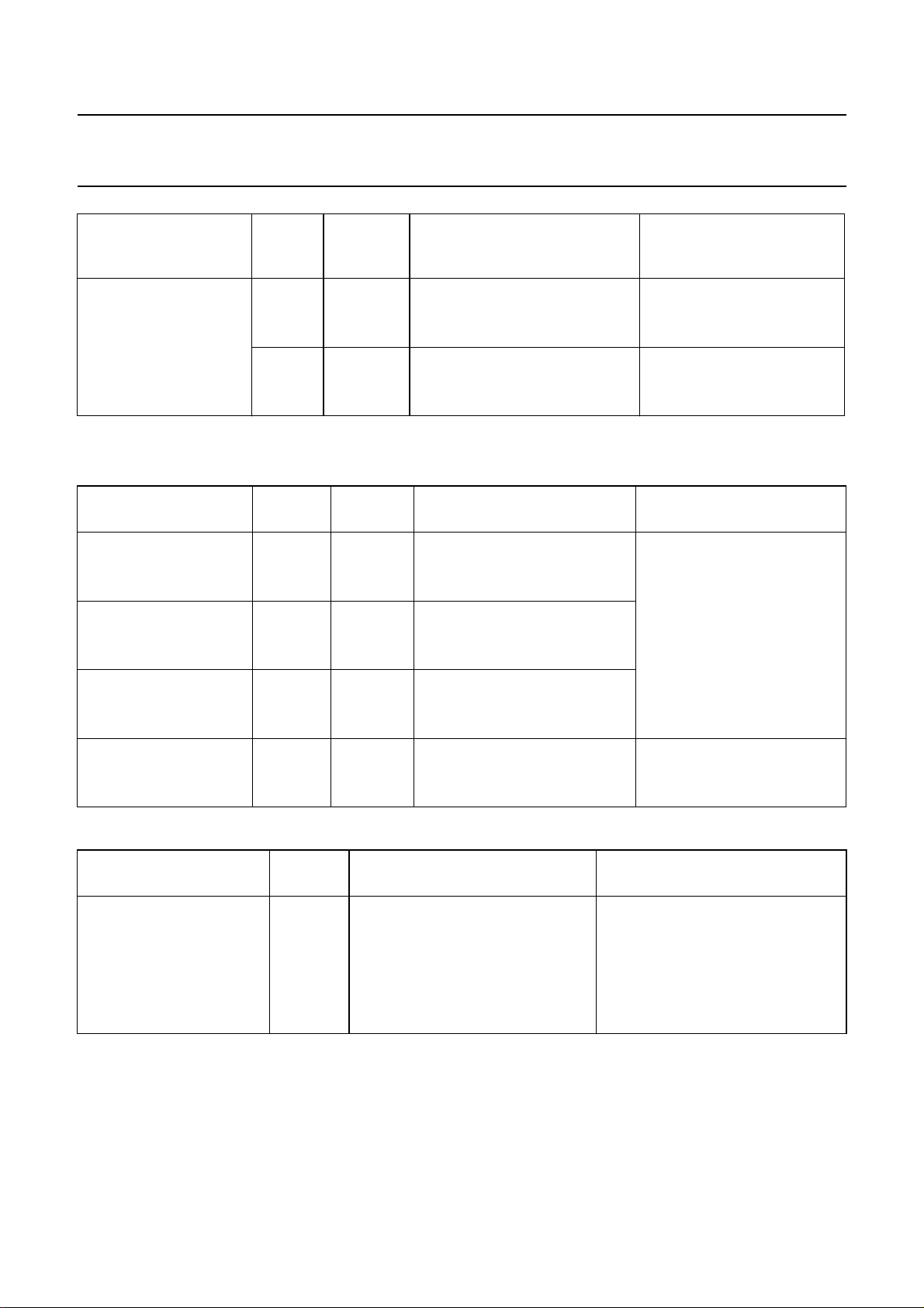
Output transition times 5 60 120 ns 10 ns + (1,0 ns/pF) C
HIGH to LOW 10 t
THL
30 60 ns 9 ns + (0,42 ns/pF) C
15 20 40 ns 6 ns + (0,28 ns/pF) C
5 60 120 ns 10 ns + (1,0 ns/pF) C
LOW to HIGH 10 t
TLH
30 60 ns 9 ns + (0,42 ns/pF) C
15 20 40 ns 6 ns + (0,28 ns/pF) C
AC CHARACTERISTICS
V
= 0 V; T
SS
Minimum I
width; HIGH 10 t
=25°C; CL= 50 pF; input transition times ≤ 20 ns
amb
V
DD
V
pulse 5 80 40 ns
2
SYMBOL MIN. TYP. MAX.
WI2H
40 20 ns
15 30 15 ns
Minimum MR 5 70 35 ns
pulse width; HIGH 10 t
WMRH
40 20 ns
15 30 15 ns
Recovery time 5 20 −10 ns
for MR 10 t
RMR
15 −5ns
15 15 0 ns
Maximum clock 5 6 12 MHz
pulse frequency 10 f
max
12 25 MHz
15 17 35 MHz
TYPICAL
EXTRAPOLATION
FORMULA
see also waveforms
Fig.5
L
L
L
L
L
L
V
DD
V
Dynamic power 5 1 200 f
dissipation per 10 5 100 f
package (P) 15 13 050 f
TYPICAL FORMULA FOR P (µW)
+∑ (foCL) × V
i
+∑(foCL) × V
i
+∑(foCL) × V
i
January 1995 6
DD
DD
DD
2
2
2
where
fi= input freq. (MHz)
fo= output freq. (MHz)
C
= load capacitance (pF)
L
∑ (f
) = sum of outputs
oCL
V
= supply voltage (V)
DD
Page 7
Philips Semiconductors Product specification
24-stage frequency divider and oscillator
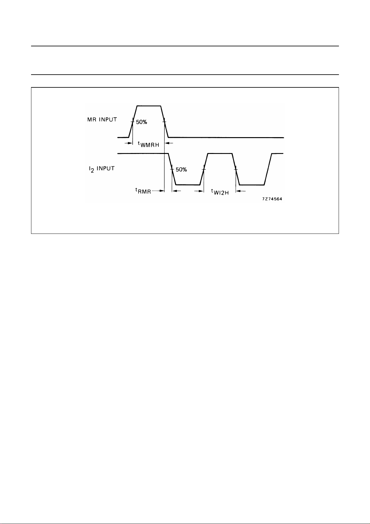
Fig.5 Waveforms showing minimum pulse widths for MR and I2, recovery time for MR.
HEF4521B
MSI
January 1995 7
Page 8
Philips Semiconductors Product specification
24-stage frequency divider and oscillator
APPLICATION INFORMATION
HEF4521B
MSI
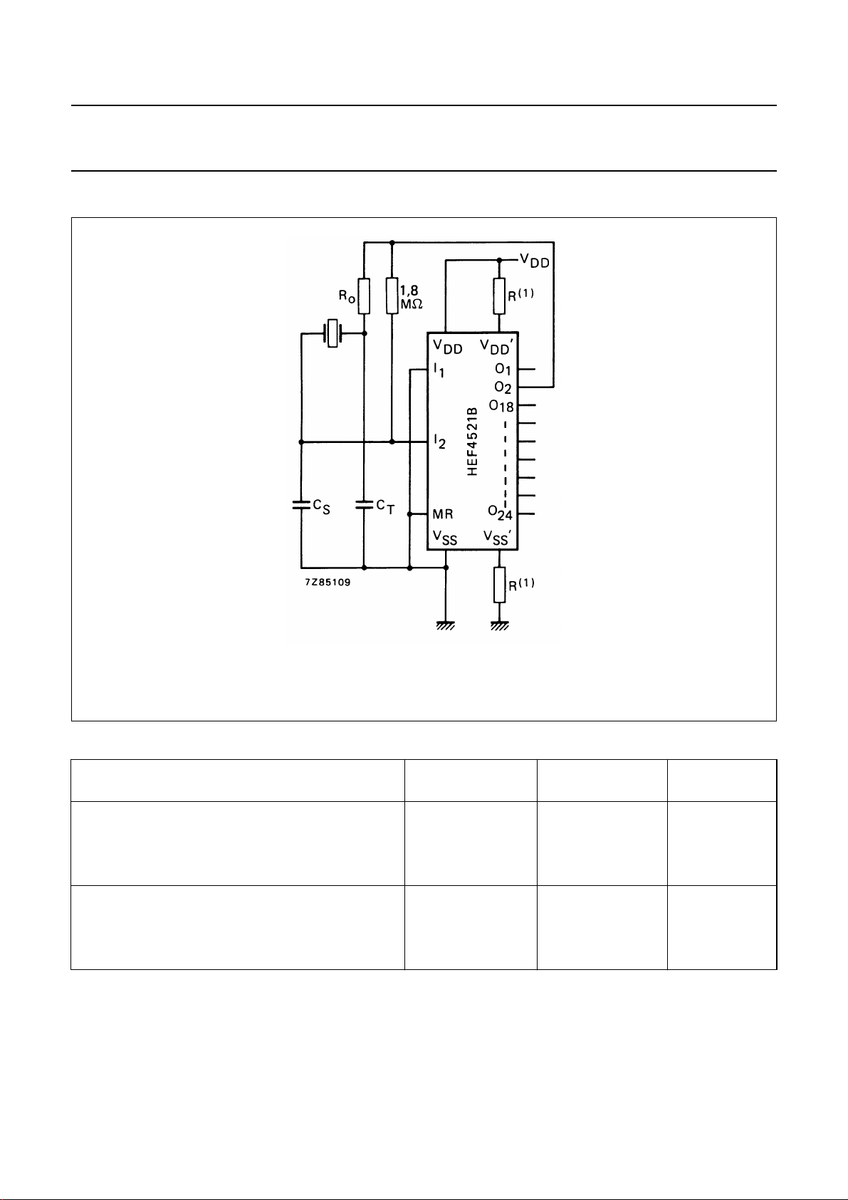
(1) Optional for low power operation.
Fig.6 Crystal oscillator circuit.
Typical characteristics for crystal oscillator circuit (Fig.6):
500 kHz
CIRCUIT
Crystal characteristics
resonance frequency 500 50 kHz
crystal cut S N −
equivalent resistance; R
External resistor/capacitor values
R
o
C
T
C
S
S
1 6,2 kΩ
47 750 kΩ
82 82 pF
20 20 pF
50 kHz
CIRCUIT
UNIT
January 1995 8
Page 9
Philips Semiconductors Product specification
24-stage frequency divider and oscillator
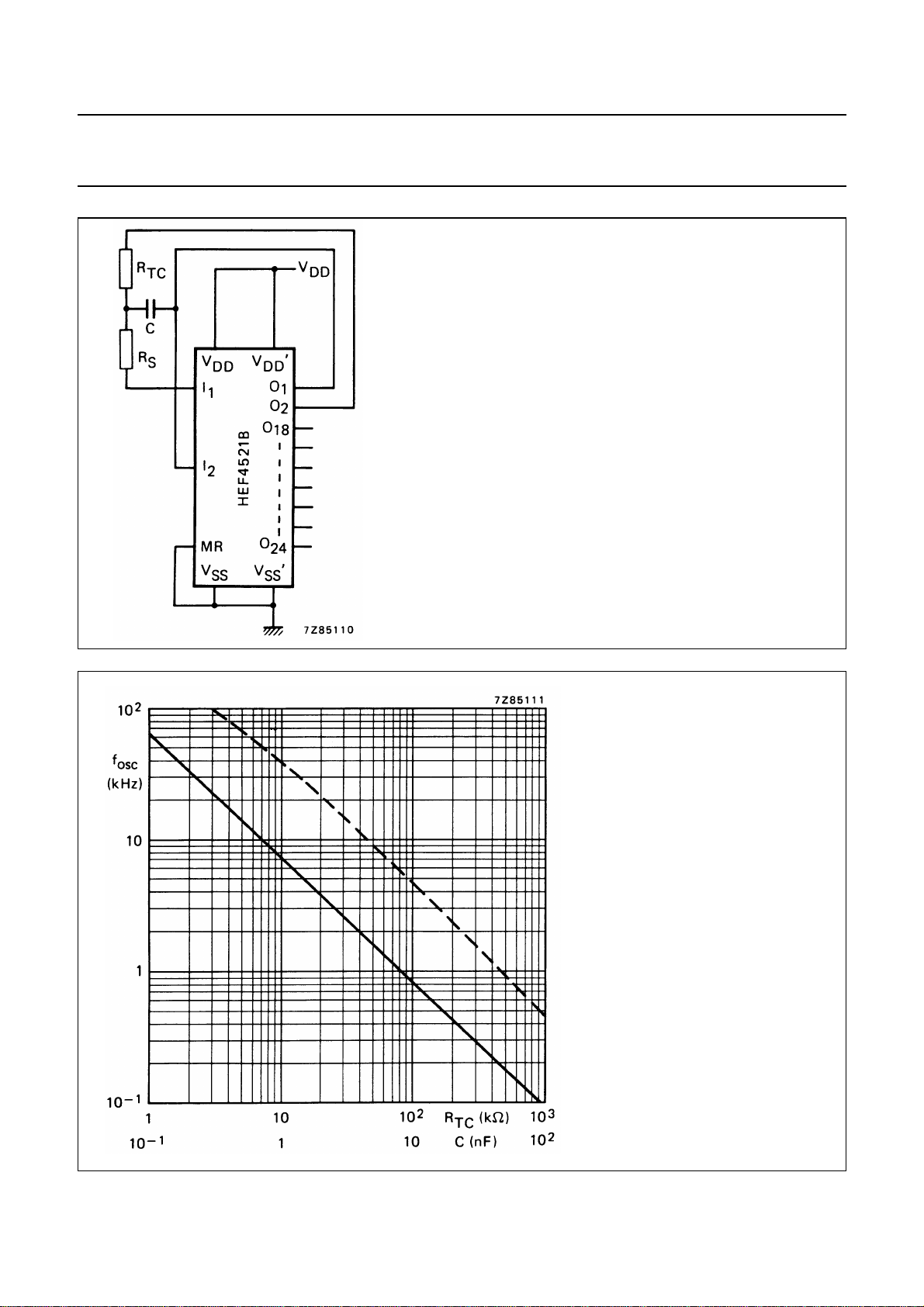
Fig.7 RC oscillator circuit;
1
------------------------------------
f
2,3 R
R
SRTC
TC
f in Hz, R in Ω, C in F.
V
------------------
<+
C××
IL max
I
LI
;R
HEF4521B
MSI
2RTCin which:,≥≈
S
maximum input voltage LOW()
input leakage current()
January 1995 9
RTC; C = 1 nF; RS≈ 2 R
C; RTC= 56 kΩ; RS= 120 kΩ
TC
Fig.8 Oscillator frequency as a
function of RTCand C;
VDD= 10 V; test circuit is
Fig.7.
Page 10
Philips Semiconductors Product specification
24-stage frequency divider and oscillator
HEF4521B
MSI
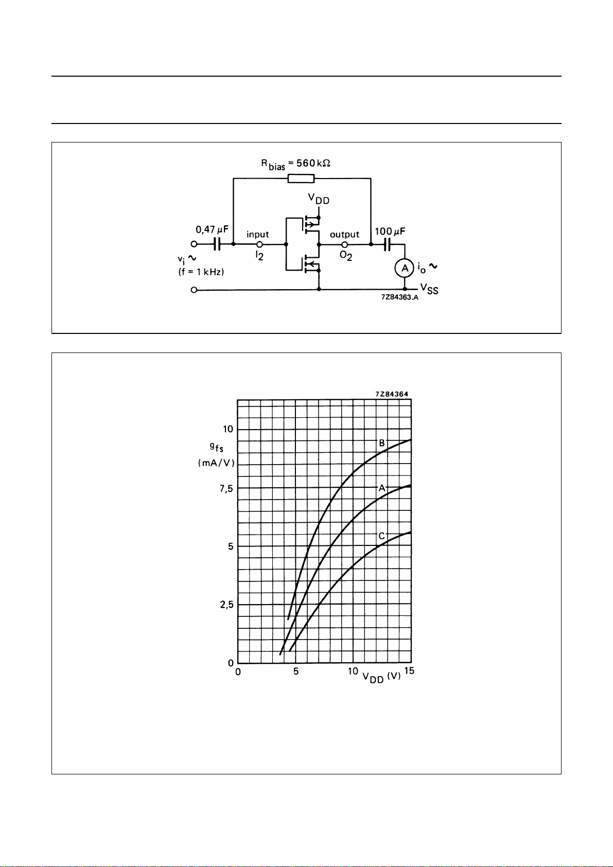
Fig.9 Test set-up for measuring forward transconductance gfs=dio/dviat vois constant (see also graph Fig.10).
A: average,
B: average + 2 s,
C: average − 2 s, in which: ‘s’ is the observed standard deviation.
Fig.10 Typical forward transconductance gfsas a function of the supply voltage at T
January 1995 10
amb
=25°C.
Page 11
Philips Semiconductors Product specification
24-stage frequency divider and oscillator
HEF4521B
MSI
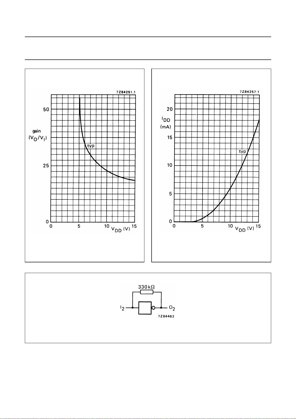
Fig.11 Voltage gain VO/VIas a function of supply
voltage.
Fig.13 Test set-up for measuring graphs of Figs 11 and 12.
January 1995 11
Fig.12 Supply current as a function of supply
voltage.
 Loading...