

Page 1

DATA SH EET
Product specification
File under Integrated Circuits, IC04
January 1995
INTEGRATED CIRCUITS
HEF4519B
MSI
Quadruple 2-input multiplexer
For a complete data sheet, please also download:
•The IC04 LOCMOS HE4000B Logic
Family Specifications HEF, HEC
•The IC04 LOCMOS HE4000B Logic
Package Outlines/Information HEF, HEC
Page 2
January 1995 2
Philips Semiconductors Product specification
Quadruple 2-input multiplexer
HEF4519B
MSI
DESCRIPTION
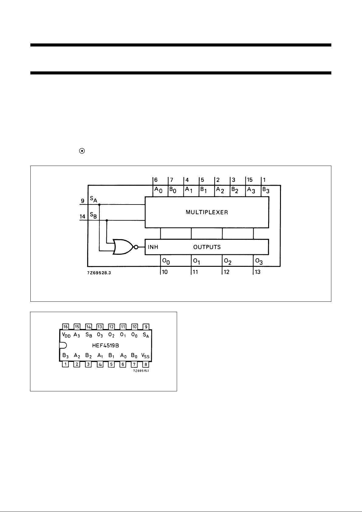
The HEF4519B provides four multiplexing circuits with
common select inputs (SA, SB); each circuit contains two
inputs (An, Bn) and one output (On). It may be used to
select four bits of information from one of two sources.
The ‘A’ inputs are selected when SAis HIGH, the ‘B’ inputs
when SBis HIGH. When SAand SBare HIGH, the output
(On) is the logical EXCLUSIVE-NOR of the Anand
Bninputs (On= A
n
Bn).
When SAand SBare LOW, the output (On) is LOW,
independent of the multiplexer inputs (Anand Bn).
The HEF4519B cannot be used to multiplex analogue
signals. The outputs utilize standard buffers for best
performance.
Fig.1 Functional diagram.
HEF4519BP(N): 16-lead DIL; plastic (SOT38-1)
HEF4519BD(F): 16-lead DIL; ceramic (cerdip)
(SOT74)
HEF4519BT(D): 16-lead SO; plastic (SOT109-1)
( ): Package Designator North America
Fig.2 Pinning diagram.
PINNING
FAMILY DATA, I
DD
LIMITS category MSI
See Family Specifications
S
A,SB
selects inputs (active HIGH)
A
0
to A
3
multiplexer inputs
B
o
to B
3
multiplexer inputs
O
0
to O
3
multiplexer outputs
Page 3

January 1995 3
Philips Semiconductors Product specification
Quadruple 2-input multiplexer
HEF4519B
MSI
FUNCTION TABLE
Notes
1. H = HIGH state (the more positive voltage)
L = LOW state (the less positive voltage)
X = state is immaterial
INPUTS OUTPUT
S
A
S
B
A
n
B
n
O
n
LLXX L
HLA
n
XA
n
LHXB
n
B
n
HHLL H
HHHL L
HHLH L
HHHH H
Fig.3 Logic diagram.
Page 4

January 1995 4
Philips Semiconductors Product specification
Quadruple 2-input multiplexer
HEF4519B
MSI
AC CHARACTERISTICS
V
SS
= 0 V; T
amb
=25°C; CL= 50 pF; input transition times ≤ 20 ns
APPLICATION INFORMATION
Some examples of applications for the HEF4519B are:
• 2-input multiplexers.
• True/complement selectors.
V
DD
V
SYMBOL TYP. MAX.
TYPICAL EXTRAPOLATION
FORMULA
Propagation delays
An,Bn→O
n
5 95 190 ns 68 ns + (0,55 ns/pF) C
L
HIGH to LOW 10 t
PHL
40 80 ns 29 ns + (0,23 ns/pF) C
L
15 30 60 ns 22 ns + (0,16 ns/pF) C
L
5 80 160 ns 53 ns + (0,55 ns/pF) C
L
LOW to HIGH 10 t
PLH
40 80 ns 29 ns + (0,23 ns/pF) C
L
15 30 60 ns 22 ns + (0,16 ns/pF) C
L
SA, SB→ O
n
5 95 190 ns 68 ns + (0,55 ns/pF) C
L
HIGH to LOW 10 t
PHL
40 80 ns 29 ns + (0,23 ns/pF) C
L
15 30 55 ns 22 ns + (0,16 ns/pF) C
L
5 85 165 ns 58 ns + (0,55 ns/pF) C
L
LOW to HIGH 10 t
PLH
40 80 ns 29 ns + (0,23 ns/pF) C
L
15 30 60 ns 22 ns + (0,16 ns/pF) C
L
Output transition times 5 60 120 ns 10 ns + (1,0 ns/pF) C
L
HIGH to LOW 10 t
THL
30 60 ns 9 ns + (0,42 ns/pF) C
L
15 20 40 ns 6 ns + (0,28 ns/pF) C
L
5 60 120 ns 10 ns + (1,0 ns/pF) C
L
LOW to HIGH 10 t
TLH
30 60 ns 9 ns + (0,42 ns/pF) C
L
15 20 40 ns 6 ns + (0,28 ns/pF) C
L
V
DD
V
TYPICAL FORMULA FOR P (µW)
Dynamic power 5 1000 f
i
+∑(foCL) × V
DD
2
where
dissipation per 10 6000 f
i
+∑(foCL) × V
DD
2
fi= input freq. (MHz)
package (P) 15 17 000 f
i
+∑(foCL) × V
DD
2
fo= output freq. (MHz)
C
L
= load capacitance (pF)
∑ (f
oCL
) = sum of outputs
V
DD
= supply voltage (V)
 Loading...