

Page 1

DATA SH EET
Product specification
File under Integrated Circuits, IC04
January 1995
INTEGRATED CIRCUITS
HEF4517B
LSI
Dual 64-bit static shift register
For a complete data sheet, please also download:
•The IC04 LOCMOS HE4000B Logic
Family Specifications HEF, HEC
•The IC04 LOCMOS HE4000B Logic
Package Outlines/Information HEF, HEC
Page 2
January 1995 2
Philips Semiconductors Product specification
Dual 64-bit static shift register
HEF4517B
LSI
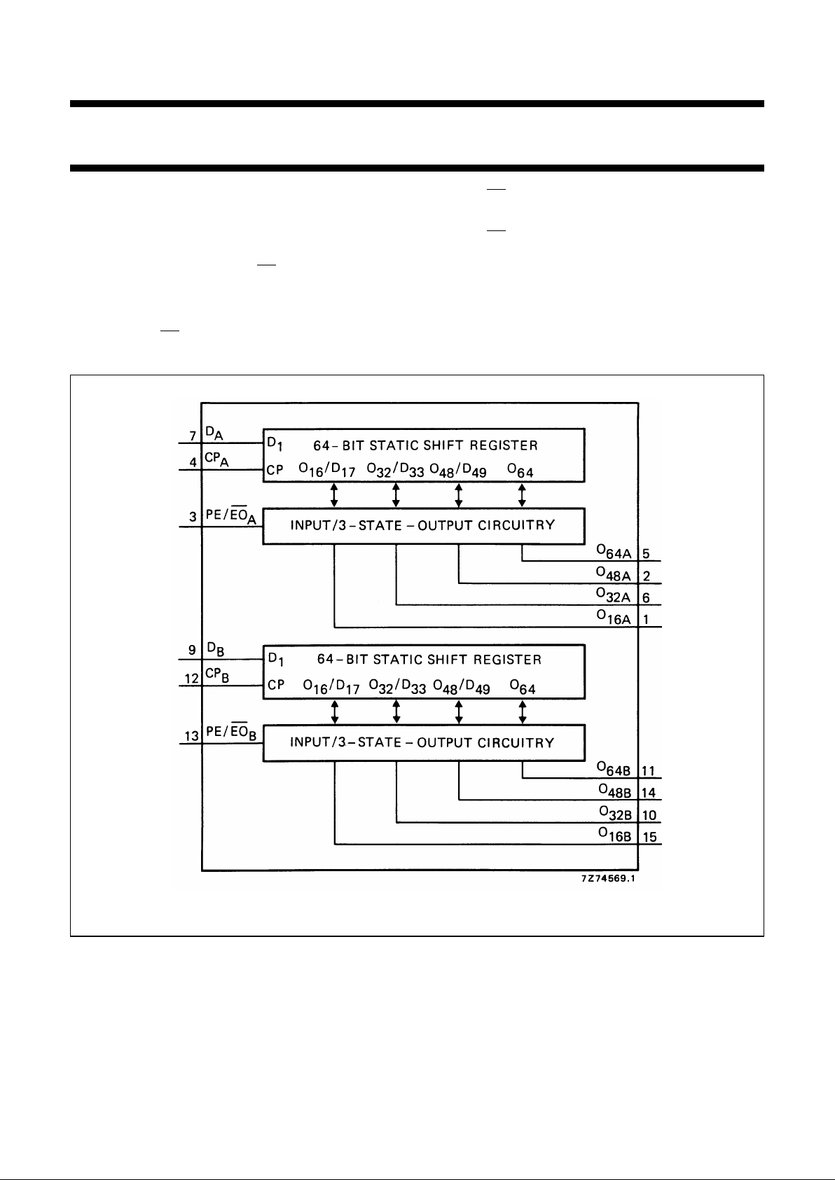
DESCRIPTION
The HEF4517B consists of two identical, independent
64-bit static shift registers. Each register has separate
clock (CP), data input (D), parallel
input-enable/output-enable (PE/EO) and four 3-state
outputs of the 16th, 32nd, 48th and 64th bit positions
(O16to O64). Data at the D input is entered into the first bit
on the LOW to HIGH transition of the clock, regardless of
the state of PE/EO.
When PE/
EO is LOW the outputs are enabled and the
device is in the 64-bit serial mode.
When PE/EO is HIGH the outputs are disabled (high
impedance OFF-state), the 64-bit shift register is divided
into four 16-bit shift registers with D, O16, O32and O48as
data inputs of the 1st, 17th, 33rd, and 49th bit respectively.
Schmitt-trigger action in the clock input makes the circuit
highly tolerant to slower clock rise and fall times.
FAMILY DATA, I
DD
LIMITS category LSI
See Family Specifications
Fig.1 Functional diagram.
Page 3
January 1995 3
Philips Semiconductors Product specification
Dual 64-bit static shift register
HEF4517B
LSI
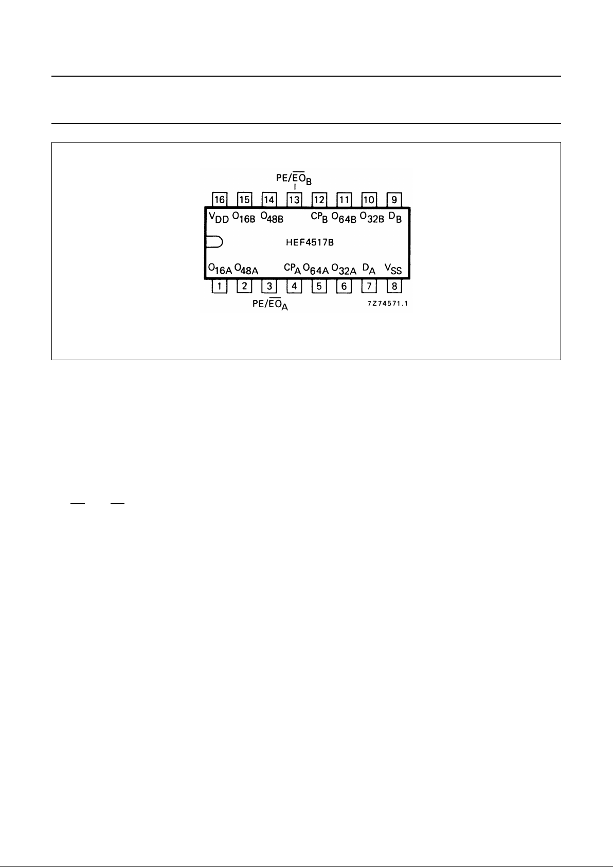
PINNING
HEF4517BP(N): 16-lead DIL; plastic (SOT38-1)
HEF4517BD(F): 16-lead DIL; ceramic (cerdip) (SOT74)
HEF4517BT(D): 16-lead SO; plastic (SOT109-1)
( ): Package Designator North America
CP
A
, CP
B
clock inputs
PE/
EOA, PE/EO
B
parallel input-enable/output-enable inputs
D
A
, D
B
data inputs
O
16A
, O
32A
, O
48A
3-state outputs/inputs
O
16B
, O
32B
, O
48B
3-state outputs/inputs
O
64A
, O
64B
3-state outputs
Fig.2 Pinning diagram.
Page 4

January 1995 4
Philips Semiconductors Product specification
Dual 64-bit static shift register
HEF4517B
LSI
This text is here in white to force landscape pages to be rotated correctly when browsing through the pdf in the Acrobat reader.This text is here in
_white to force landscape pages to be rotated correctly when browsing through the pdf in the Acrobat reader.This text is here inThis text is here in
white to force landscape pages to be rotated correctly when browsing through the pdf in the Acrobat reader. white to force landscape pages to be ...
Fig.3 Logic diagram (one shift register).
Page 5

January 1995 5
Philips Semiconductors Product specification
Dual 64-bit static shift register
HEF4517B
LSI
This text is here in white to force landscape pages to be rotated correctly when browsing through the pdf in the Acrobat reader.This text is here in
_white to force landscape pages to be rotated correctly when browsing through the pdf in the Acrobat reader.This text is here inThis text is here in
white to force landscape pages to be rotated correctly when browsing through the pdf in the Acrobat reader. white to force landscape pages to be ...
FUNCTION TABLE
Notes
1. H = HIGH state (the more positive voltage)
L = LOW state (the less positive voltage)
X = state is immaterial
Z = high impedance state
= positive-going transition
= negative-going transition
INPUTS INPUTS/OUTPUTS
MODE
CP D PE/
EO O
16
O
32
O
48
O
64
data entered
into 1st bit
L content of
16th bit
displayed
content of
32nd bit
displayed
content of
48th bit
displayed
content of
64th bit
displayed
One 64-bit shift
register. The content of the
shift register is
shifted over one stage
data entered
into 1st bit
H data at
O
16
entered
into 17th bit
data at
O32entered into
33rd bit
data at
O48entered
into 49th bit
remains in
‘Z’ state
Four 16-bit shift
register. The content of
the shift registers is
shifted over one stage.
X L no change no change no change no change no change
X H Z Z Z Z no change
Page 6

January 1995 6
Philips Semiconductors Product specification
Dual 64-bit static shift register
HEF4517B
LSI
AC CHARACTERISTICS
V
SS
= 0 V; T
amb
=25°C; input transition times ≤ 20 ns
AC CHARACTERISTICS
V
SS
= 0 V; T
amb
=25°C; CL= 50 pF; input transition times ≤ 20 ns
V
DD
V
TYPICAL FORMULA FOR P (µW)
Dynamic power 5 7 000 f
i
+∑(foCL) × V
DD
2
where
dissipation per 10 28 000 f
i
+∑(foCL) × V
DD
2
fi= input freq. (MHz)
package (P) 15 70 000 f
i
+∑(foCL) × V
DD
2
fo= output freq. (MHz)
C
L
= load capacitance (pF)
∑ (f
oCL
) = sum of outputs
V
DD
= supply voltage (V)
V
DD
V
SYMBOL MIN. TYP. MAX.
TYPICAL EXTRAPOLATION
FORMULA
Propagation delays
CP → O
n
5 220 440 ns 193 ns + (0,55 ns/pF) C
L
HIGH to LOW 10 t
PHL
85 170 ns 74 ns + (0,23 ns/pF) C
L
15 60 120 ns 52 ns + (0,16 ns/pF) C
L
5 190 380 ns 163 ns + (0,55 ns/pF) C
L
LOW to HIGH 10 t
PLH
75 150 ns 64 ns + (0,23 ns/pF) C
L
15 50 100 ns 42 ns + (0,16 ns/pF) C
L
Output transition
times 5 60 120 ns 10 ns + (1,0 ns/pF) C
L
HIGH to LOW 10 t
THL
30 60 ns 9 ns + (0,42 ns/pF) C
L
15 20 40 ns 6 ns + (0,28 ns/pF) C
L
5 60 120 ns 10 ns + (1,0 ns/pF) C
L
LOW to HIGH 10 t
TLH
30 60 ns 9 ns + (0,42 ns/pF) C
L
15 20 40 ns 6 ns + (0,28 ns/pF) C
L
Page 7

January 1995 7
Philips Semiconductors Product specification
Dual 64-bit static shift register
HEF4517B
LSI
AC CHARACTERISTICS
V
SS
= 0 V; T
amb
=25°C; CL= 50 pF; input transition times ≤ 20 ns
V
DD
V
SYMBOL MIN. TYP. MAX.
Minimum clock 5 95 190 ns
see also waveforms
Fig.4.
pulse width; LOW 10 t
WCPL
40 80 ns
15 30 60 ns
Set-up times 5 30 10 ns
O
n
, D → CP 10 t
su
25 5 ns
15 20 5 ns
Hold time 5 45 15 ns
O
n
, D → CP 10 t
hold
30 10 ns
15 25 10 ns
3-state propagation
delays
Output disable times
PE/
EO → O
n
54080ns
HIGH 10 t
PHZ
30 60 ns
15 25 50 ns
5 50 100 ns
LOW 10 t
PLZ
30 60 ns
15 25 50 ns
Output enable times
PE/
EO → O
n
54590ns
HIGH 10 t
PZH
25 50 ns
15 20 40 ns
5 60 120 ns
LOW 10 t
PZL
30 60 ns
15 25 50 ns
Maximum clock 5 2 5 MHz
pulse frequency 10 f
max
6 12 MHz
15 8 16 MHz
Page 8

January 1995 8
Philips Semiconductors Product specification
Dual 64-bit static shift register
HEF4517B
LSI
Fig.4 Waveforms showing minimum clock pulse width, set-up and hold times for On(as data input) and D to CP.
 Loading...