

Page 1

DATA SH EET
Product specification
File under Integrated Circuits, IC04
January 1995
INTEGRATED CIRCUITS
HEF4511B
MSI
BCD to 7-segment
latch/decoder/driver
For a complete data sheet, please also download:
•The IC04 LOCMOS HE4000B Logic
Family Specifications HEF, HEC
•The IC04 LOCMOS HE4000B Logic
Package Outlines/Information HEF, HEC
Page 2

January 1995 2
Philips Semiconductors Product specification
BCD to 7-segment latch/decoder/driver
HEF4511B
MSI
DESCRIPTION
The HEF4511B is a BCD to 7-segment
latch/decoder/driver with four address inputs (DAto DD),
an active LOW latch enable input (EL), an active LOW
ripple blanking input (BI), an active LOW lamp test input
(LT), and seven active HIGH n-p-n bipolar transistor
segment outputs (Oato Og).
When
EL is LOW, the state of the segment outputs (Oato
Og) is determined by the data on DAto DD.
When EL goes HIGH, the last data present on DAto
DDare stored in the latches and the segment outputs
remain stable. When LT is LOW, all the segment outputs
are HIGH independent of all other input conditions. With
LT HIGH, a LOW on BI forces all segment outputs LOW.
The inputs LT and BI do not affect the latch circuit.
Fig.1 Functional diagram.
PINNING
HEF4511BP(N): 16-lead DIL; plastic (SOT38-1)
HEF4511BD(F): 16-lead DIL; ceramic (cerdip) (SOT74)
HEF4511BT(D): 16-lead SO; plastic (SOT109-1)
( ): Package Designator North America
D
A
to D
D
address (data) inputs
EL latch enable input (active LOW)
BI ripple blanking input (active LOW)
LT lamp test input (active LOW)
O
a
to O
g
segment outputs
Fig.2 Pinning diagram.
Fig.3 Schematic diagram of output stage.
FAMILY DATA, IDDLIMITS category MSI
See Family Specifications
Fig.4 Segment
designation.
Page 3
January 1995 3
Philips Semiconductors Product specification
BCD to 7-segment latch/decoder/driver
HEF4511B
MSI
This text is here in white to force landscape pages to be rotated correctly when browsing through the pdf in the Acrobat reader.This text is here in
_white to force landscape pages to be rotated correctly when browsing through the pdf in the Acrobat reader.This text is here inThis text is here in
white to force landscape pages to be rotated correctly when browsing through the pdf in the Acrobat reader. white to force landscape pages to be ...
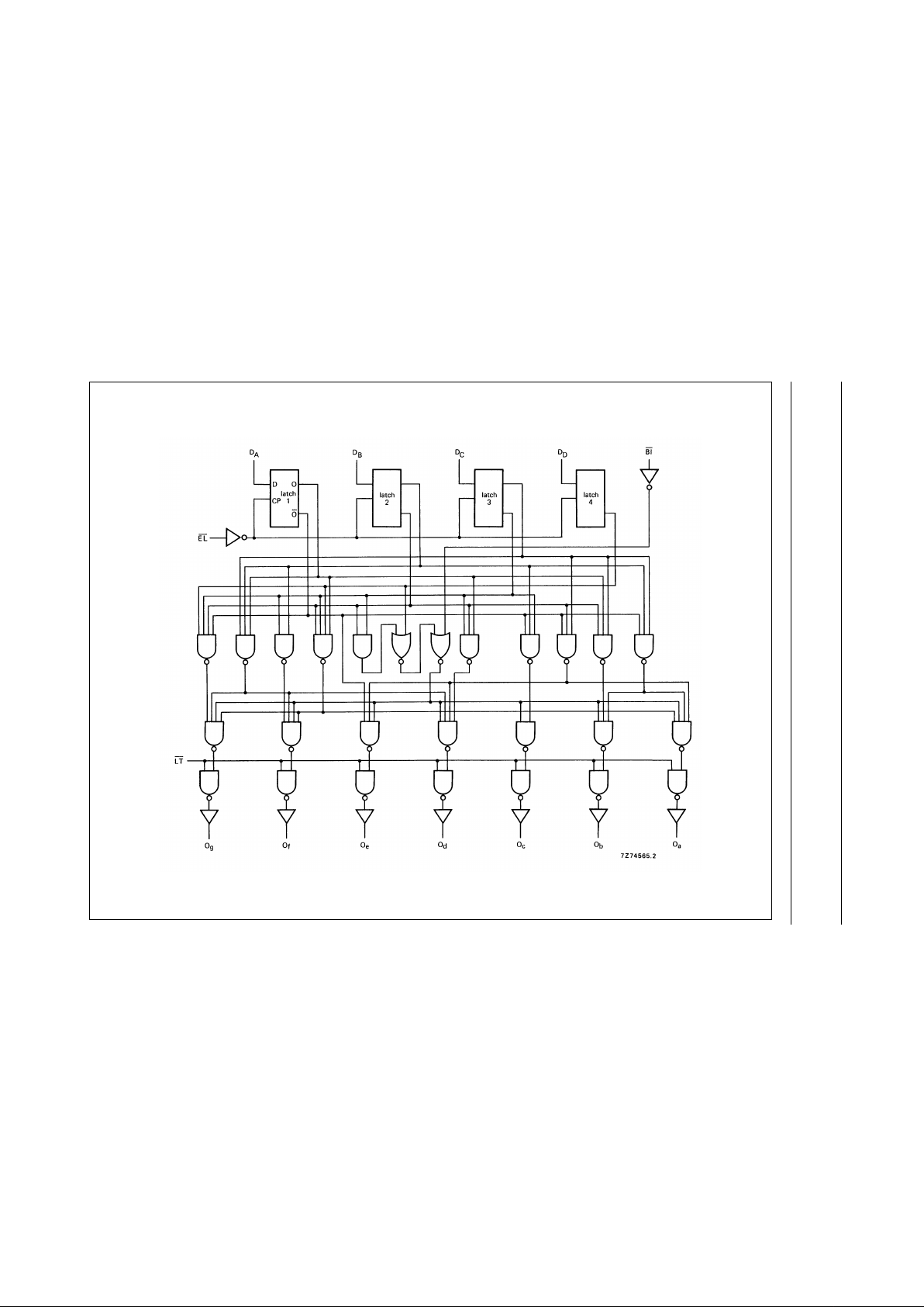
Fig.5 Logic diagram; for one latch see Fig.6.
Page 4

January 1995 4
Philips Semiconductors Product specification
BCD to 7-segment latch/decoder/driver
HEF4511B
MSI
FUNCTION TABLE
Note
1. H = HIGH state (the more positive voltage)
L = LOW state (the less positive voltage)
X = state is immaterial
* Depends upon the BCD code applied during the LOW to HIGH transition of
EL.
INPUTS OUTPUTS
EL BI LTDDDCDBDAOaObOcOdOeOfOgDISPLAY
XXLXXXXHH HHHHH 8
X L H X X X X L L L L L L L blank
LHHL L L LHHHHHHL 0
LHHLLLHLHHLLLL 1
LHHLLHLHHLHHLH 2
LHHL L H H H H H H L L H 3
LHHLHLLLHHLLHH 4
LHHLHLHHLHHLHH 5
LHHLHH LL L HHHHH 6
LHHLHHHHHHLLLL 7
LHHHL L LHH HHHHH 8
LHHH L L H H H H L L HH 9
L H H H L H L L L L L L L L blank
L H H H L H H L L L L L L L blank
L H H H H L L L L L L L L L blank
L H H H H L H L L L L L L L blank
L H H H H H L L L L L L L L blank
L H H H H H H L L L L L L L blank
HHHX X X X * *
Fig.6 Logic diagram (one latch); see also Fig.5.
Page 5

January 1995 5
Philips Semiconductors Product specification
BCD to 7-segment latch/decoder/driver
HEF4511B
MSI
RATINGS
Limiting values in accordance with the Absolute Maximum System (IEC 134).
Note
1. A destructive high current mode may occur if V
I
and VOare not constrained to the range VSS≤ VIor VO≤ VDD.
Output (source) current HIGH −I
OH
max. 25 mA
For other RATINGS see Family Specifications.
Fig.7 Display.
Page 6

January 1995 6
Philips Semiconductors Product specification
BCD to 7-segment latch/decoder/driver
HEF4511B
MSI
DC CHARACTERISTICS
V
SS
=0 V
HEF
V
DD
V
I
OH
mA
SYMBOL
T
amb
(°C)
−40 + 25 + 85
MIN. MAX. MIN. TYP. MIN. MAX.
Output voltage 5 0 4,10 4,10 4,40 4,10 V
HIGH 10 0 V
OH
9,10 9,10 9,40 9,10 V
15 0 14,10 14,10 14,40 14,10 V
Output voltage 5 5 4,20 V
HIGH 10 5 V
OH
9,20 V
15 5 14,20 V
Output voltage 5 10 3,60 3,60 4,05 3,30 V
HIGH 10 10 V
OH
8,75 8,75 9,10 8,45 V
15 10 13,75 13,75 14,10 13,45 V
Output voltage 5 15 4,00 V
HIGH 10 15 V
OH
9,00 V
15 15 14,00 V
Output voltage 5 20 2,80 2,80 3,80 2,50 V
HIGH 10 20 V
OH
8,10 8,10 9,00 7,80 V
15 20 13,10 13,10 14,00 12,80 V
Output voltage 5 25 3,70 V
HIGH 10 25 V
OH
8,90 V
15 25 14,00 V
Page 7

January 1995 7
Philips Semiconductors Product specification
BCD to 7-segment latch/decoder/driver
HEF4511B
MSI
AC CHARACTERISTICS
V
SS
= 0 V; T
amb
=25°C; input transition times ≤ 20 ns
HEC
V
DD
V
I
OH
mA
SYMBOL
T
amb
(°C)
−55 + 25 + 125
MIN. MAX. MIN. TYP. MIN. MAX.
Output voltage 5 0 4,10 4,10 4,40 4,10 V
HIGH 10 0 V
OH
9,10 9,10 9,90 9,10 V
15 0 14,10 14,10 14,40 14,40 V
Output voltage 5 5 4,30 V
HIGH 10 5 V
OH
9,30 V
15 5 14,30 V
Output voltage 5 10 3,60 3,60 4,25 3,20 V
HIGH 10 10 V
OH
8,75 8,75 9,25 8,35 V
15 10 13,75 13,75 14,25 13,35 V
Output voltage 5 15 4,20 V
HIGH 10 15 V
OH
9,20 V
15 15 14,20 V
Output voltage 5 20 2,80 2,80 4,20 2,30 V
HIGH 10 20 V
OH
8,10 8,10 9,20 7,60 V
15 20 13,10 13,10 14,20 12,60 V
Output voltage 5 25 4,15 V
HIGH 10 25 V
OH
9,20 V
15 25 14,20 V
V
DD
V
TYPICAL FORMULA FOR P (µW)
Dynamic power 5 1 000 f
i
+∑(foCL) × V
DD
2
where
dissipation per 10 4 000 f
i
+∑(foCL) × V
DD
2
fi= input freq. (MHz)
package (P) 15 10 000 f
i
+∑(foCL) × V
DD
2
fo= output freq. (MHz)
C
L
= load capacitance (pF)
∑ (f
oCL
) = sum of outputs
V
DD
= supply voltage (V)
Page 8

January 1995 8
Philips Semiconductors Product specification
BCD to 7-segment latch/decoder/driver
HEF4511B
MSI
AC CHARACTERISTICS
V
SS
= 0 V; T
amb
=25°C; CL= 50 pF; input transition times ≤ 20 ns
V
DD
V
SYMBOL MIN. TYP. MAX.
TYPICAL EXTRAPOLATION
FORMULA
Propagation delays
Dn→ O
n
5 155 310 ns 128 ns + (0,55 ns/pF) C
L
HIGH to LOW 10 t
PHL
60 120 ns 49 ns + (0,23 ns/pF) C
L
15 40 80 ns 32 ns + (0,16 ns/pF) C
L
5 135 270 ns 108 ns + (0,55 ns/pF) C
L
LOW to HIGH 10 t
PLH
55 110 ns 44 ns + (0,23 ns/pF) C
L
15 40 80 ns 32 ns + (0,16 ns/pF) C
L
EL → O
n
5 160 320 ns 133 ns + (0,55 ns/pF) C
L
HIGH to LOW 10 t
PHL
60 120 ns 49 ns + (0,23 ns/pF) C
L
15 45 90 ns 37 ns + (0,16 ns/pF) C
L
5 160 320 ns 133 ns + (0,55 ns/pF) C
L
LOW to HIGH 10 t
PLH
70 140 ns 59 ns + (0,23 ns/pF) C
L
15 50 100 ns 42 ns + (0,16 ns/pF) C
L
BI → O
n
5 120 240 ns 93 ns + (0,55 ns/pF) C
L
HIGH to LOW 10 t
PHL
50 100 ns 39 ns + (0,23 ns/pF) C
L
15 35 70 ns 27 ns + (0,16 ns/pF) C
L
BI → O
n
5 105 210 ns 78 ns + (0,55 ns/pF) C
L
LOW to HIGH 10 t
PLH
40 80 ns 29 ns + (0,23 ns/pF) C
L
15 30 60 ns 22 ns + (0,16 ns/pF) C
L
LT → O
n
5 80 160 ns 52 ns + (0,55 ns/pF) C
L
HIGH to LOW 10 t
PHL
30 60 ns 19 ns + (0,23 ns/pF) C
L
15 20 40 ns 12 ns + (0,16 ns/pF) C
L
5 60 120 ns 33 ns + (0,55 ns/pF) C
L
LOW to HIGH 10 t
PLH
30 60 ns 19 ns + (0,23 ns/pF) C
L
15 25 50 ns 17 ns + (0,16 ns/pF) C
L
Output transition times 5 60 120 ns 10 ns + (1,0 ns/pF) C
L
HIGH to LOW 10 t
THL
30 60 ns 9 ns + (0,42 ns/pF) C
L
15 20 40 ns 6 ns + (0,28 ns/pF) C
L
5 25 50 ns 20 ns + (1,0 na/pF) C
L
LOW to HIGH 10 t
TLH
16 32 ns 13 ns + (0,06 ns/pF) C
L
15 13 26 ns 10 ns + (0,06 ns/pF) C
L
Page 9

January 1995 9
Philips Semiconductors Product specification
BCD to 7-segment latch/decoder/driver
HEF4511B
MSI
Minimum EL 5 80 40 ns
see also waveforms
Fig.8
pulse width; LOW 10 t
WELL
40 20 ns
15 35 17 ns
Set-up time 5 50 25 ns
D
n
→ EL 10 t
su
25 12 ns
15 20 9 ns
Hold-time 5 60 30 ns
D
n
→ EL 10 t
hold
30 15 ns
15 25 12 ns
V
DD
V
SYMBOL MIN. TYP. MAX.
TYPICAL EXTRAPOLATION
FORMULA
Fig.8 Waveforms showing minimum EL pulse width, set-up and hold time for DC to EL.
Conditions:
DD= LOW
DA=DB=BI=LT = HIGH
Page 10

January 1995 10
Philips Semiconductors Product specification
BCD to 7-segment latch/decoder/driver
HEF4511B
MSI
APPLICATION INFORMATION
Some examples of applications for the HEF4511B are:
• Driving LED displays.
• Driving incandescent displays.
• Driving fluorescent displays.
• Driving LCD displays.
• Driving gas discharge displays.
Fig.9 Connection to common cathode LED display readout.
Fig.10 Connection to common anode LED display readout.
Page 11

January 1995 11
Philips Semiconductors Product specification
BCD to 7-segment latch/decoder/driver
HEF4511B
MSI
Fig.11 Connection to incandescent display readout.
(1) A filament pre-warm resistor is recommended to
reduce filament thermal shock and increase the
effective cold resistance of the filament.
Fig.12 Connection to fluorescent display readout.
Fig.13 Connection to gas discharge display
readout.
Fig.14 Connection to liquid crystal (LCD) display
readout. Direct d.c. drive of LCDs not
recommended for life of LCD readouts.
 Loading...