

Page 1

DATA SH EET
Product specification
File under Integrated Circuits, IC04
January 1995
INTEGRATED CIRCUITS
HEF4505B
LSI
64-bit, 1-bit per word random
access read/write memory
For a complete data sheet, please also download:
•The IC04 LOCMOS HE4000B Logic
Family Specifications HEF, HEC
•The IC04 LOCMOS HE4000B Logic
Package Outlines/Information HEF, HEC
Page 2
January 1995 2
Philips Semiconductors Product specification
64-bit, 1-bit per word random access
read/write memory
HEF4505B
LSI
DESCRIPTION
The HEF4505B is a 64-bit, 1-bit per word, fully decoded
and completely static, random access memory. The
memory is strobed for reading or writing only when the
strobe input (ST), chip enable inputs (CE1and CE2) are
HIGH simultaneously. The output data is available at the
data output (D
OUT
) only when the memory is strobed, the
read/write input (R/W) is HIGH and after the read access
time has passed. Note that the three-state output is initially
disabled and always goes to the LOW state before data is
valid. The output is disabled in the high-impedance
OFF-state, when the memory is not strobed or R/
W is
LOW. R/W may remain HIGH during a read cycle or LOW
during a write cycle. The output data has the same polarity
as the input data.
HEF4505BP(N): 14-lead DIL; plastic
(SOT27-1)
HEF4505BD(F): 14-lead DIL; ceramic (cerdip)
(SOT73)
( ): Package Designator North America
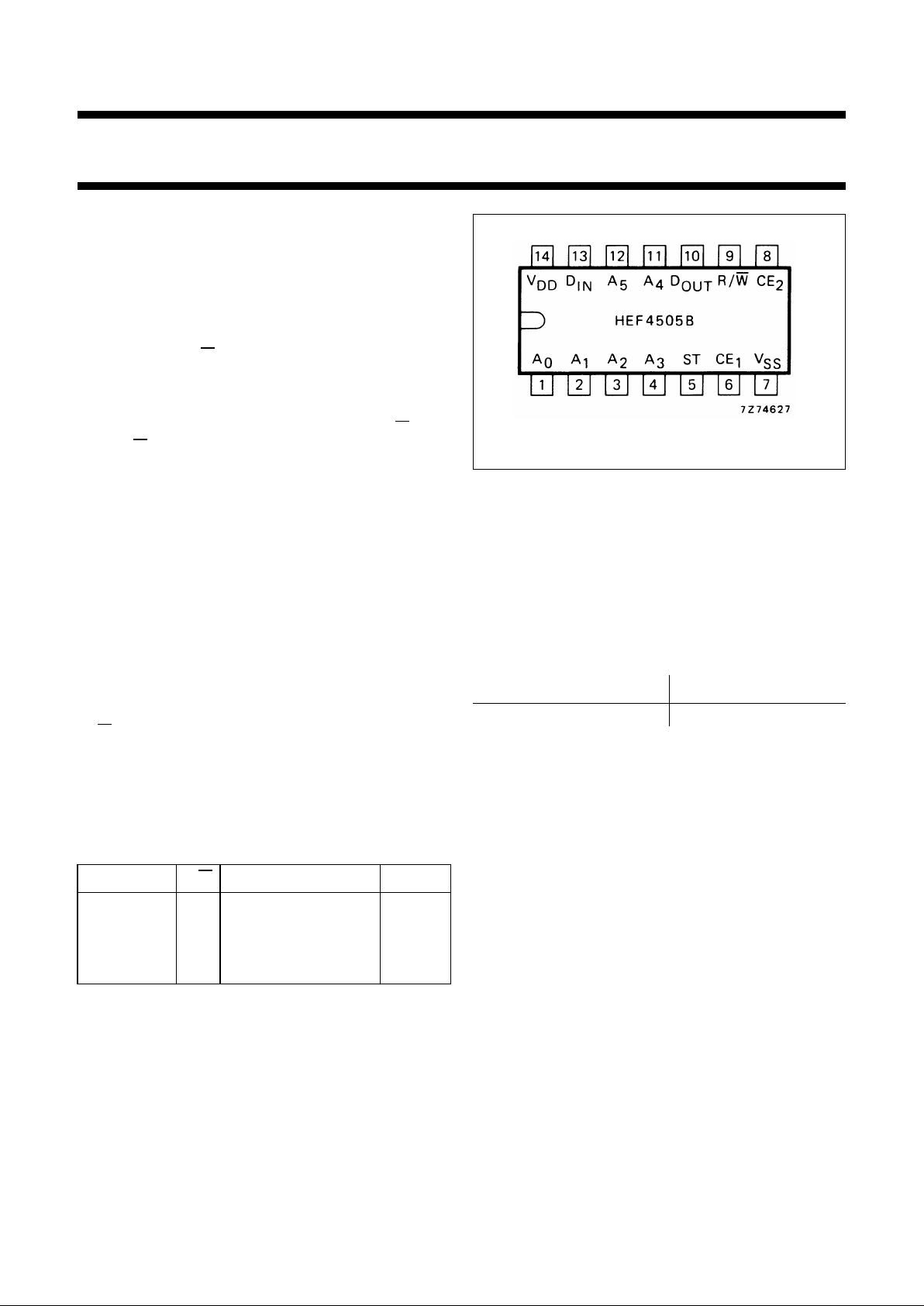
Fig.1 Pinning diagram.
PINNING
FUNCTION TABLE
Note
1. H = HIGH state (the more positive voltage)
L = LOW state (the less positive voltage)
Z = high-impedance OFF-state
A
0
to A
5
address inputs
CE
1
,CE
2
chip enable inputs
R/
W read/write input
ST strobe input
D
IN
data input
D
OUT
data output
ST, CE
1
,CE2R/WD
OUT
MODE
L L Z disabled
H L Z write
L H Z disabled
H H equal to memory data read
SUPPLY VOLTAGE
Note
1. Minimum standby voltage for data retention is 3 V.
FAMILY DATA, I
DD
LIMITS category LSI
See Family Specifications
RATING OPERATING
−0,5 to +15 4,5 to 15 V
Page 3
January 1995 3
Philips Semiconductors Product specification
64-bit, 1-bit per word random access
read/write memory
HEF4505B
LSI
This text is here in white to force landscape pages to be rotated correctly when browsing through the pdf in the Acrobat reader.This text is here in
_white to force landscape pages to be rotated correctly when browsing through the pdf in the Acrobat reader.This text is here inThis text is here in
white to force landscape pages to be rotated correctly when browsing through the pdf in the Acrobat reader. white to force landscape pages to be ...
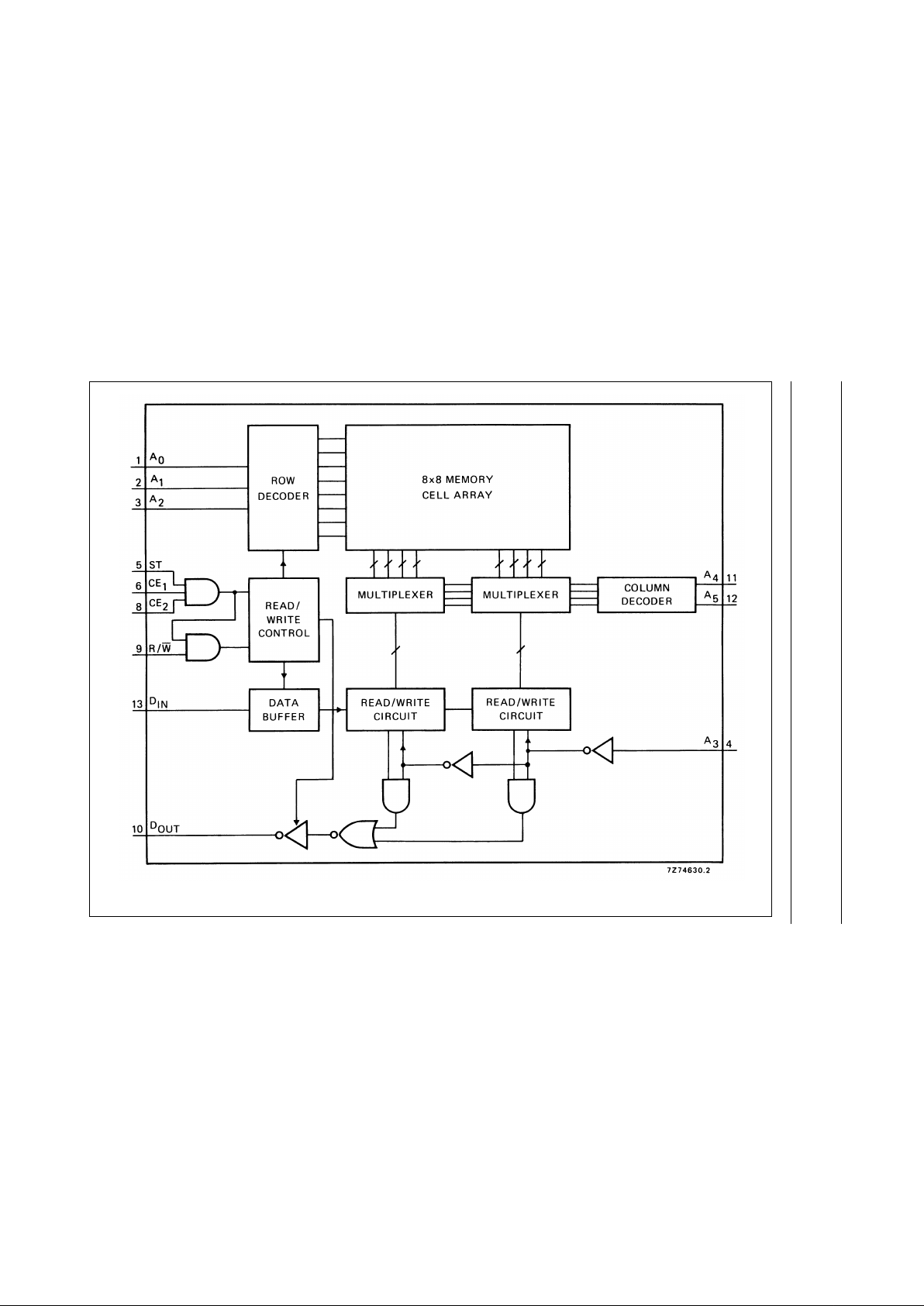
Fig.2 Functional diagram.
Page 4

January 1995 4
Philips Semiconductors Product specification
64-bit, 1-bit per word random access
read/write memory
HEF4505B
LSI
AC CHARACTERISTICS
V
SS
= 0 V; T
amb
=25°C; CL= 50 pF; input transition times ≤ 20 ns
V
DD
V
SYMBOL MIN. TYP. MAX.
TYPICAL EXTRAPOLATION
FORMULA
Minimum strobe pulse 5 75 35 ns
width; LOW 10 t
STL
45 22 ns
15 30 15 ns
5 350 700 ns
Read cycle time 10 t
RC
250 500 ns
15 210 420 ns
5 220 440 ns
Write cycle time 10 t
WC
125 250 ns
15 75 150 ns
5 330 660 ns 303 ns + (0,55 ns/pF) C
L
Read access time 10 t
ACC
135 270 ns 124 ns + (0,23 ns/pF) C
L
15 100 200 ns 92 ns + (0,16 ns/pF) C
L
58040ns
Address recovery time 10 t
AR
40 20 ns
15 25 10 ns
5 180 90 ns
Read recovery time 10 t
RR
120 60 ns
15 90 45 ns
57535ns
Write recovery time 10 t
WR
45 25 ns
15 40 20 ns
3-state propagation delays
5
t
PHZ
,
t
PLZ
105 210 ns
Output disable times 10 60 125 ns
15 55 115 ns
Set-up times 5 −20 −40 ns
A
n
→ ST 10 t
suA
−10 −20 ns
15 −5 −10 ns
5 −30 −60 ns
R/
W → ST 10 t
suR
−15 −30 ns
15 −5 −10 ns
5 160 80 ns
D
IN
→ ST 10 t
suD
75 35 ns
15 45 20 ns
5 240 120 ns
R/
W → ST 10 t
suW
100 50 ns
15 75 35 ns
Page 5

January 1995 5
Philips Semiconductors Product specification
64-bit, 1-bit per word random access
read/write memory
HEF4505B
LSI
Hold time 5 −20 −40 ns
D
IN
→ ST 10 t
holdD
5 −10 ns
15 10 0 ns
V
DD
V
SYMBOL MIN. TYP. MAX.
TYPICAL EXTRAPOLATION
FORMULA
Fig.3 Read cycle timing diagram.
(1) Output in high impedance OFF-state.
(2) t
STHmin=tRCmax
− t
STLmin
.
Page 6

January 1995 6
Philips Semiconductors Product specification
64-bit, 1-bit per word random access
read/write memory
HEF4505B
LSI
Fig.4 Write cycle timing diagram.
(1) t
STHmin=tWCmax
− t
STLmin.
Page 7

January 1995 7
Philips Semiconductors Product specification
64-bit, 1-bit per word random access
read/write memory
HEF4505B
LSI
APPLICATION INFORMATION
Fig.5 256-word by n-bit static read/write memory using HEF4505B ICs.
Page 8

January 1995 8
Philips Semiconductors Product specification
64-bit, 1-bit per word random access
read/write memory
HEF4505B
LSI
Figure 5 shows a 256-word by n-bit static RAM system.
The outputs of the four HEF4505B circuits are tied
together to form 256 words by 1-bit. Additional bits are
attained by paralleling the inputs in groups of four.
Memories of larger words can be attained by decoding the
most significant bits of the address and AND-ing them with
the strobe input.
Fan-in and fan-out of the memory are limited only by speed
requirements. The extremely low input and output leakage
currents keep the output voltage levels from changing
significantly as more outputs are tied together. With the
output levels independent of fan-out, most of the power
supply range is available as logic swing, regardless of the
number of units wired together. As a result, high noise
immunity is maintained under all conditions.
The memory system shown in Fig.5 can be interfaced
directly with other ICs of the LOCMOS HE family. No
external components are required.
Non-volatile information storage is allowed due to very low
power dissipation when the memory is powered by a small
standby battery. Figure 6 shows an optional standby
power supply circuit for making a LOCMOS memory
‘non-volatile’. When the usual power fails, a battery is used
to sustain operation or maintain stored information. While
normal power supply voltage is present, the battery is
trickle-charged through a resistor (R) which sets the
charging rate. In Fig.6 the sustaining voltage is VB, and + V
is the ordinary voltage from a power supply. VDDis
connected to the power supply pin of the memory.
Low-leakage diodes are recommended to conserve
battery power.
Fig.6 Standby battery circuit.
 Loading...