

Page 1

DATA SH EET
Product specification
File under Integrated Circuits, IC04
January 1995
INTEGRATED CIRCUITS
HEF4094B
MSI
8-stage shift-and-store bus register
For a complete data sheet, please also download:
•The IC04 LOCMOS HE4000B Logic
Family Specifications HEF, HEC
•The IC04 LOCMOS HE4000B Logic
Package Outlines/Information HEF, HEC
Page 2
January 1995 2
Philips Semiconductors Product specification
8-stage shift-and-store bus register
HEF4094B
MSI
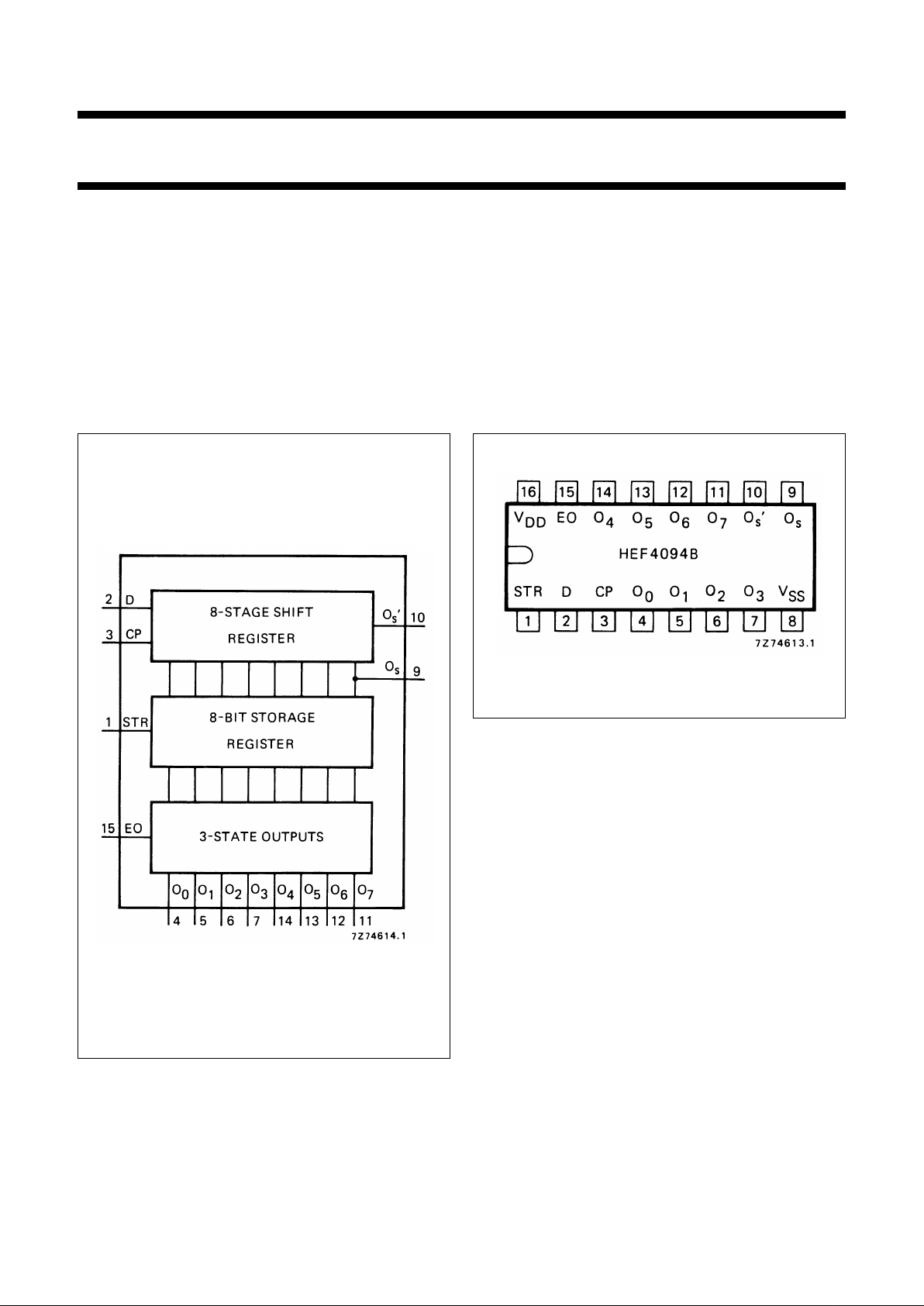
DESCRIPTION
The HEF4094B is an 8-stage serial shift register having a
storage latch associated with each stage for strobing data
from the serial input to parallel buffered 3-state outputs
O0to O7. The parallel outputs may be connected directly
to common bus lines. Data is shifted on positive-going
clock transitions. The data in each shift register stage is
transferred to the storage register when the strobe (STR)
input is HIGH. Data in the storage register appears at the
outputs whenever the output enable (EO) signal is HIGH.
Two serial outputs (O
s
and O’s) are available for cascading
a number of HEF4094B devices. Data is available at Oson
positive-going clock edges to allow high-speed operation
in cascaded systems in which the clock rise time is fast.
The same serial information is available at O’son the next
negative-going clock edge and provides cascading
HEF4094B devices when the clock rise time is slow.
Fig.1 Functional diagram.
PINNING
FAMILY DATA, IDDLIMITS category MSI
See Family Specifications
HEF4094BP(N): 16-lead DIL; plastic
(SOT38-1)
HEF4094BD(F): 16-lead DIL; ceramic (cerdip)
(SOT74)
HEF4094BT(D): 16-lead SO; plastic
(SOT109-1)
( ): Package Designator North America
D data input EO output enable input
CP clock input O
s
, O’
s
serial outputs
STR strobe input O
0
to O7parallel outputs
Fig.2 Pinning diagram.
Page 3
January 1995 3
Philips Semiconductors Product specification
8-stage shift-and-store bus register
HEF4094B
MSI
This text is here in white to force landscape pages to be rotated correctly when browsing through the pdf in the Acrobat reader.This text is here in
_white to force landscape pages to be rotated correctly when browsing through the pdf in the Acrobat reader.This text is here inThis text is here in
white to force landscape pages to be rotated correctly when browsing through the pdf in the Acrobat reader. white to force landscape pages to be ...
Fig.3 Logic diagram.
Fig.4 One D-latch.
Page 4

January 1995 4
Philips Semiconductors Product specification
8-stage shift-and-store bus register
HEF4094B
MSI
FUNCTION TABLE
Notes
1. H = HIGH state (the more positive voltage)
2. L = LOW state (the less positive voltage)
3. X = state is immaterial
4. = positive-going transition
5. = negative-going transition
6. Z = high impedance off state
7. nc = no change
8. O’
6
= the information in the seventh shift register stage
At the positive clock edge the information in the 7th register stage is transferred to the 8th register stage and the
Osoutput.
AC CHARACTERISTICS
V
SS
= 0 V; T
amb
=25°C; input transition times ≤ 20 ns
INPUTS PARALLEL OUTPUTS SERIAL OUTPUTS
CP EO STR D O
0
O
n
O
s
O’
s
LXX Z Z O’
6
nc
LXX Z Z nc O
7
HLX nc nc O’
6
nc
HH L L O
n-1
O’
6
nc
HHH H O
n-1
O’
6
nc
HHH nc nc nc O
7
V
DD
V
TYPICAL FORMULA FOR P (µW)
Dynamic power 5 2100 f
i
+∑(foCL) × V
DD
2
where
dissipation per 10 9700 f
i
+∑(foCL) × V
DD
2
fi= input freq. (MHz)
package (P) 15 26 000 f
i
+∑(foCL) × V
DD
2
fo= output freq. (MHz)
C
L
= load capacitance (pF)
∑ (f
oCL
) = sum of outputs
V
DD
= supply voltage (V)
Page 5

January 1995 5
Philips Semiconductors Product specification
8-stage shift-and-store bus register
HEF4094B
MSI
AC CHARACTERISTICS
V
SS
= 0 V; T
amb
=25°C; CL= 50 pF; input transition times ≤ 20 ns
V
DD
V
SYMBOL TYP. MAX.
TYPICAL EXTRAPOLATION
FORMULA
Propagation delays
CP → O
s
5 135 270 ns 108 ns + (0,55 ns/pF) C
L
HIGH to LOW 10 t
PHL
65 130 ns 54 ns + (0,23 ns/pF) C
L
15 50 100 ns 42 ns + (0,16 ns/pF) C
L
5 105 210 ns 78 ns + (0,55 ns/pF) C
L
LOW to HIGH 10 t
PLH
50 100 ns 39 ns + (0,23 ns/pF) C
L
15 40 80 ns 32 ns + (0,16 ns/pF) C
L
CP → O’
s
5 105 210 ns 78 ns + (0,55 ns/pF) C
L
HIGH to LOW 10 t
PHL
50 100 ns 39 ns + (0,23 ns/pF) C
L
15 40 80 ns 32 ns + (0,16 ns/pF) C
L
5 105 210 ns 78 ns + (0,55 ns/pF) C
L
LOW to HIGH 10 t
PLH
50 100 ns 39 ns + (0,23 ns/pF) C
L
15 40 80 ns 32 ns + (0,16 ns/pF) C
L
CP → O
n
5 165 330 ns 138 ns + (0,55 ns/pF) C
L
HIGH to LOW 10 t
PHL
75 150 ns 64 ns + (0,23 ns/pF) C
L
15 55 110 ns 47 ns + (0,16 ns/pF) C
L
5 150 300 ns 123 ns + (0,55 ns/pF) C
L
LOW to HIGH 10 t
PLH
70 140 ns 59 ns + (0,23 ns/pF) C
L
15 55 110 ns 47 ns + (0,16 ns/pF) C
L
STR → O
n
5 110 220 ns 83 ns + (0,55 ns/pF) C
L
HIGH to LOW 10 t
PHL
50 100 ns 39 ns + (0,23 ns/pF) C
L
15 35 70 ns 27 ns + (0,16 ns/pF) C
L
5 100 200 ns 73 ns + (0,55 ns/pF) C
L
LOW to HIGH 10 t
PLH
45 90 ns 34 ns + (0,23 ns/pF) C
L
15 35 70 ns 27 ns + (0,16 ns/pF) C
L
Output transition times 5 60 120 ns 10 ns + (1,0 ns/pF) C
L
HIGH to LOW 10 t
THL
30 60 ns 9 ns + (0,42 ns/pF) C
L
15 20 40 ns 6 ns + (0,28 ns/pF) C
L
5 60 120 ns 10 ns + (1,0 ns/pF) C
L
LOW to HIGH 10 t
TLH
30 60 ns 9 ns + (0,42 ns/pF) C
L
15 20 40 ns 6 ns + (0,28 ns/pF) C
L
Page 6

January 1995 6
Philips Semiconductors Product specification
8-stage shift-and-store bus register
HEF4094B
MSI
AC CHARACTERISTICS
V
SS
= 0 V; T
amb
=25°C; CL= 50 pF; input transition times ≤ 20 ns
V
DD
V
SYMBOL MIN. TYP. MAX.
3-state propagation delays
Output enable times 5 40 80 ns
EO → O
n
10 t
PZH
25 50 ns
HIGH 15 20 40 ns
54080ns
LOW 10 t
PZL
25 50 ns
15 20 40 ns
Output disable times 5 75 150 ns
EO → O
n
10 t
PHZ
40 80 ns
HIGH 15 30 60 ns
5 80 160 ns
LOW 10 t
PLZ
40 80 ns
15 30 60 ns
Minimum clock 5 60 30 ns
pulse width 10 t
WCPL
30 15 ns
LOW 15 24 12 ns
Minimum strobe 5 40 20 ns
pulse width 10 t
WSTRH
30 15 ns
HIGH 15 24 12 ns
Set-up times 5 60 30 ns
D → CP 10 t
su
20 10 ns
15 15 5 ns
Hold times 5 5 −15 ns
D → CP 10 t
hold
20 5 ns
15 20 5 ns
Maximum clock 5 5 10 MHz
pulse frequency 10 f
max
11 22 MHz
15 14 28 MHz
Page 7

January 1995 7
Philips Semiconductors Product specification
8-stage shift-and-store bus register
HEF4094B
MSI
APPLICATION INFORMATION
Some examples of applications for the HEF4094B are:
• Serial-to-parallel data conversion
• Remote control holding register
Fig.5 Timing diagram.
Fig.6 Remote control holding register.
 Loading...