

Page 1

DATA SH EET
Product specification
File under Integrated Circuits, IC04
January 1995
INTEGRATED CIRCUITS
HEF4093B
gates
Quadruple 2-input NAND Schmitt
trigger
For a complete data sheet, please also download:
•The IC04 LOCMOS HE4000B Logic
Family Specifications HEF, HEC
•The IC04 LOCMOS HE4000B Logic
Package Outlines/Information HEF, HEC
Page 2
January 1995 2
Philips Semiconductors Product specification
Quadruple 2-input NAND Schmitt trigger
HEF4093B
gates
DESCRIPTION
The HEF4093B consists of four Schmitt-trigger circuits.
Each circuit functions as a two-input NAND gate with
Schmitt-trigger action on both inputs. The gate switches at
different points for positive and negative-going signals.
The difference between the positive voltage (VP) and the
negative voltage (VN) is defined as hysteresis voltage
(VH).
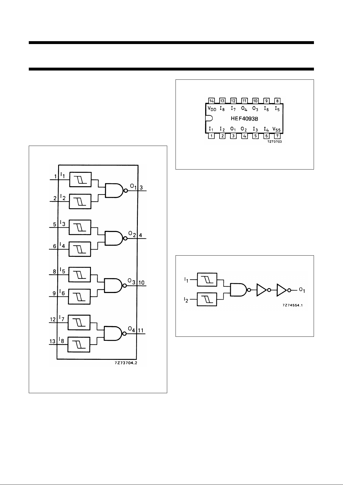
Fig.1 Functional diagram.
FAMILY DATA, IDDLIMITS category GATES
See Family Specifications
HEF4093BP(N): 14-lead DIL; plastic
(SOT27-1)
HEF4093BD(F): 14-lead DIL; ceramic (cerdip)
(SOT73)
HEF4093BT(D): 14-lead SO; plastic
(SOT108-1)
( ): Package Designator North America
Fig.2 Pinning diagram.
Fig.3 Logic diagram (one gate).
Page 3

January 1995 3
Philips Semiconductors Product specification
Quadruple 2-input NAND Schmitt trigger
HEF4093B
gates
DC CHARACTERISTICS
V
SS
= 0 V; T
amb
=25°C
V
DD
V
SYMBOL MIN. TYP. MAX.
Hysteresis 5 0,4 0,7 − V
voltage 10 V
H
0,6 1,0 − V
15 0,7 1,3 − V
Switching levels 5 1,9 2,9 3,5 V
positive-going 10 V
P
3,6 5,2 7 V
input voltage 15 4,7 7,3 11 V
negative-going 5 1,5 2,2 3,1 V
input voltage 10 V
N
3 4,2 6,4 V
15 4 6,0 10,3 V
Fig.4 Transfer characteristic.
Fig.5 Waveforms showing definition of
VP,VNand VH; where VNand VPare
between limits of 30% and 70%.
Page 4

January 1995 4
Philips Semiconductors Product specification
Quadruple 2-input NAND Schmitt trigger
HEF4093B
gates
AC CHARACTERISTICS
V
SS
= 0 V; T
amb
=25°C; CL= 50 pF; input transition times ≤ 20 ns
V
DD
V
SYMBOL TYP. MAX.
TYPICAL EXTRAPOLATION
FORMULA
Propagation delays 5 90 185 ns 63 ns + (0,55 ns/pF) C
L
In→ O
n
10 t
PHL
40 80 ns 29 ns + (0,23 ns/pF) C
L
HIGH to LOW 15 30 60 ns 22 ns + (0,16 ns/pF) C
L
5 85 170 ns 58 ns + (0,55 ns/pF) C
L
LOW to HIGH 10 t
PLH
40 80 ns 29 ns + (0,23 ns/pF) C
L
15 30 60 ns 22 ns + (0,16 ns/pF) C
L
Output transition times 5 60 120 ns 10 ns + (1,0 ns/pF) C
L
HIGH to LOW 10 t
THL
30 60 ns 9 ns + (0,42 ns/pF) C
L
15 20 40 ns 6 ns + (0,28 ns/pF) C
L
5 60 120 ns 10 ns + (1,0 ns/pF) C
L
LOW to HIGH 10 t
TLH
30 60 ns 9 ns + (0,42 ns/pF) C
L
15 20 40 ns 6 ns + (0,28 ns/pF) C
L
V
DD
V
TYPICAL FORMULA FOR P (µW)
Dynamic power 5 1300 f
i
+∑(foCL) × V
DD
2
where
dissipation per 10 6400 f
i
+∑(foCL) × V
DD
2
fi= input freq. (MHz)
package (P) 15 18 700 f
i
+∑(foCL) × V
DD
2
fo= output freq. (MHz)
C
L
= load capacitance (pF)
∑ (f
oCL
) = sum of outputs
V
DD
= supply voltage (V)
Page 5

January 1995 5
Philips Semiconductors Product specification
Quadruple 2-input NAND Schmitt trigger
HEF4093B
gates
Fig.6 Typical drain current as a function of input
voltage; VDD= 5 V; T
amb
=25°C.
Fig.7 Typical drain current as a function of input
voltage; VDD=10 V; T
amb
=25°C.
Fig.8 Typical drain current as a function of input
voltage; VDD= 15 V; T
amb
=25°C.
Page 6

January 1995 6
Philips Semiconductors Product specification
Quadruple 2-input NAND Schmitt trigger
HEF4093B
gates
Fig.9 Typical switching levels as a function of supply voltage VDD;T
amb
=25°C.
APPLICATION INFORMATION
Some examples of applications for the HEF4093B are:
• Wave and pulse shapers
• Astable multivibrators
• Monostable multivibrators.
Fig.10 The HEF4093B used as a astable multivibrator.
Fig.11 Schmitt trigger driven via a high impedance
(R > 1kΩ).
If a Schmitt trigger is driven via a high impedance (R > 1 kΩ) then it is necessary to incorporate a capacitor C of such
value that:
C
p
is the external parasitic capacitance between inputs and output; the value depends on the circuit board layout.
Note
The two inputs may be connected together, but this will result in a larger through-current at the moment of switching.
C
C
p
------ -
V
DDVSS
–
V
H
---------------------------
, otherwise oscillation can occur on the edges of a pulse.>
 Loading...