

Page 1
INTEGRATED CIRCUITS
DATA SH EET
For a complete data sheet, please also download:
•The IC04 LOCMOS HE4000B Logic
Family Specifications HEF, HEC
•The IC04 LOCMOS HE4000B Logic
Package Outlines/Information HEF, HEC
HEF4086B
gates
4-wide 2-input AND-OR-invert gate
Product specification
File under Integrated Circuits, IC04
January 1995
Page 2
Philips Semiconductors Product specification
4-wide 2-input AND-OR-invert gate
DESCRIPTION
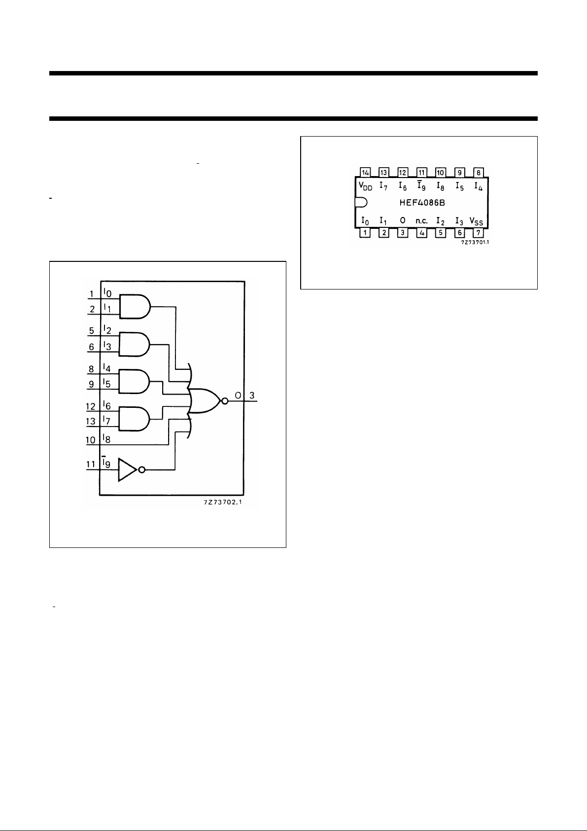
The HEF4086B is a 4-wide 2-input AND-OR-invert (AOI)
gate with two additional inputs (I8or I9) which can be used
as either expander or inhibit inputs by connecting them to
any standard LOCMOS output. A HIGH on I8or a LOW on
I9forces the output (O) LOW independent of the other
eight inputs (I0to I7). The output (O) is fully buffered for
highest noise immunity and pattern insensitivity of output
impedance.
HEF4086B
gates
Fig.2 Pinning diagram.
HEF4086BP(N): 14-lead DIL; plastic
(SOT27-1)
HEF4086BD(F): 14-lead DIL; ceramic (cerdip)
(SOT73)
HEF4086BT(D): 14-lead SO; plastic
(SOT108-1)
( ): Package Designator North America
Fig.1 Functional diagram.
PINNING
I
to I
0
I
9
O output (active LOW)
FAMILY DATA, I
See Family Specifications
January 1995 2
gate inputs
8
gate input (active LOW)
LIMITS category GATES
DD
Page 3
Philips Semiconductors Product specification
4-wide 2-input AND-OR-invert gate
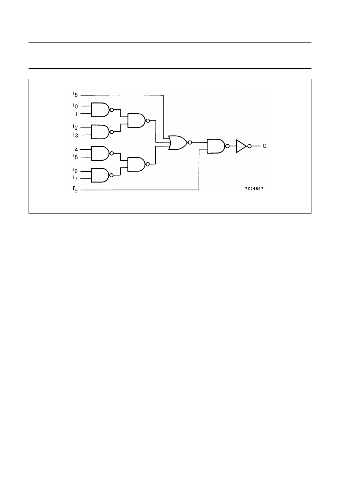
Fig.3 Logic diagram.
HEF4086B
gates
LOGIC EQUATION
OI0I1I2I3I4I5I6I7I8I
++⋅+⋅+⋅+⋅=
9
January 1995 3
Page 4
Philips Semiconductors Product specification
4-wide 2-input AND-OR-invert gate
HEF4086B
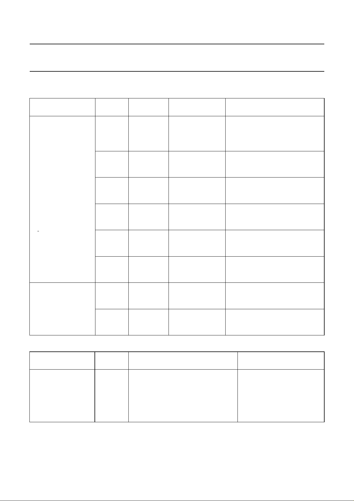
AC CHARACTERISTICS
V
= 0 V; T
SS
Propagation delays
I0to I7→ O 5 90 180 ns 63 ns + (0,55 ns/pF) C
HIGH to LOW 10 t
LOW to HIGH 10 t
I8→ O 5 70 140 ns 43 ns + (0,55 ns/pF) C
HIGH to LOW 10 t
LOW to HIGH 10 t
I9→ O 5 55 105 ns 28 ns + (0,55 ns/pF) C
HIGH to LOW 10 t
LOW to HIGH 10 t
Output transition times 5 60 120 ns 10 ns + (1,0 ns/pF) C
HIGH to LOW 10 t
LOW to HIGH 10 t
=25°C; CL= 50 pF; input transition times ≤ 20 ns
amb
V
DD
V
SYMBOL TYP. MAX.
PHL
15 20 40 ns 12 ns + (0,16 ns/pF) C
5 80 155 ns 53 ns + (0,55 ns/pF) C
PLH
15 20 40 ns 12 ns + (0,16 ns/pF) C
PHL
15 20 40 ns 12 ns + (0,16 ns/pF) C
5 55 115 ns 28 ns + (0,55 ns/pF) C
PLH
15 15 25 ns 7 ns + (0,16 ns/pF) C
PHL
15 15 30 ns 7 ns + (0,16 ns/pF) C
5 45 90 ns 18 ns + (0,55 ns/pF) C
PLH
15 10 25 ns 2 ns + (0,16 ns/pF) C
THL
15 20 40 ns 6 ns + (0,28 ns/pF) C
5 60 120 ns 10 ns + (1,0 ns/pF) C
TLH
15 20 40 ns 6 ns + (0,28 ns/pF) C
TYPICAL EXTRAPOLATION
FORMULA
30 65 ns 19 ns + (0,23 ns/pF) C
30 60 ns 19 ns + (0,23 ns/pF) C
25 55 ns 14 ns + (0,23 ns/pF) C
20 40 ns 9 ns + (0,23 ns/pF) C
20 45 ns 9 ns + (0,23 ns/pF) C
15 35 ns 4 ns + (0,23 ns/pF) C
30 60 ns 9 ns + (0,42 ns/pF) C
30 60 ns 9 ns + (0,42 ns/pF) C
gates
L
L
L
L
L
L
L
L
L
L
L
L
L
L
L
L
L
L
L
L
L
L
L
L
V
DD
V
Dynamic power 5 525 f
dissipation per 10 2600 f
package (P) 15 7300 f
TYPICAL FORMULA FOR P (µW)
+∑(foCL) × V
i
+∑(foCL) × V
i
+∑(foCL) × V
i
January 1995 4
DD
DD
DD
2
2
2
where
fi= input freq. (MHz)
fo= output freq. (MHz)
C
= load capacitance (pF)
L
∑ (f
) = sum of outputs
oCL
= supply voltage (V)
V
DD
Page 5
Philips Semiconductors Product specification
4-wide 2-input AND-OR-invert gate
APPLICATION INFORMATION
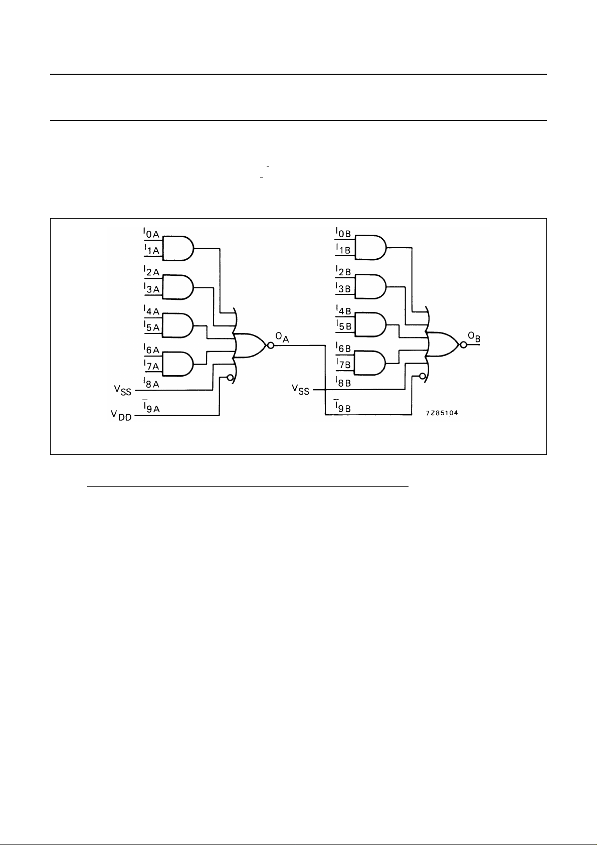
Figure 4 shows two HEF4086B ICs connected to obtain an 8-wide 2-input AOI function.
The output (OA) of the first IC is fed directly into the I9B gate input of the second IC. Similarly,
any NAND gate output can be fed directly into the I9gate input to obtain a 5-wide AOI function.
In addition, any AND gate output can be fed directly into the I8gate input with the same result.
HEF4086B
gates
Logic equation for Fig.4:
OBI0AI1AI2AI3AI4AI5AI6AI7AI0BI1BI2BI3BI4BI5BI6BI7B⋅+⋅+⋅+⋅+⋅+⋅+⋅+⋅=
Fig.4 Two HEF4086B ICs connected as an 8-wide 2-input AOI gate.
January 1995 5
 Loading...