

Page 1

DATA SH EET
Product specification
File under Integrated Circuits, IC04
January 1995
INTEGRATED CIRCUITS
HEF4076B
MSI
Quadruple D-type register with
3-state outputs
For a complete data sheet, please also download:
•The IC04 LOCMOS HE4000B Logic
Family Specifications HEF, HEC
•The IC04 LOCMOS HE4000B Logic
Package Outlines/Information HEF, HEC
Page 2
January 1995 2
Philips Semiconductors Product specification
Quadruple D-type register with 3-state outputs
HEF4076B
MSI
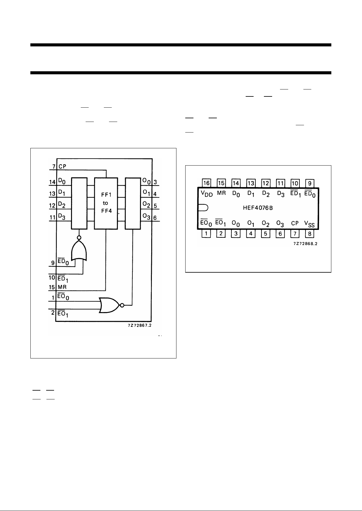
DESCRIPTION
The HEF4076B is a quadruple edge-triggered D-type
flip-flop with four data inputs (D0to D3), two active LOW
data enable inputs (ED0and ED1), a common clock input
(CP), four 3-state outputs (O0to O3), two active LOW
output enable inputs (EO0and EO1), and an overriding
asynchronous master reset input (MR).
Information on D
0
to D3is stored in the four flip-flops on the
LOW to HIGH transition of CP if both ED0and ED1are
LOW. A HIGH on either ED0or ED1prevents the flip-flops
from changing on the LOW to HIGH transition of CP,
independent of the information on D0to D3. When both
EO0and EO1are LOW, the contents of the four flip-flops
are available at O0to O3. A HIGH on either EO0or
EO1forces O0to O3into the high impedance OFF-state. A
HIGH on MR resets all four flip-flops, independent of all
other input conditions.
Fig.1 Functional diagram.
HEF4076BP(N): 16-lead DIL; plastic
(SOT38-1)
HEF4076BD(F): 16-lead DIL; ceramic (cerdip)
(SOT74)
HEF4076BT(D): 16-lead SO; plastic
(SOT109-1)
( ): Package Designator North America
Fig.2 Pinning diagram.
PINNING
D
0
to D
3
data inputs
ED0, ED
1
data enable inputs (active LOW)
EO0, EO
1
output enable inputs (active LOW)
CP clock input (LOW to HIGH, edge-triggered)
MR master reset input
O
0
to O
3
data outputs
FAMILY DATA, IDDLIMITS category MSI
See Family Specifications
Page 3
January 1995 3
Philips Semiconductors Product specification
Quadruple D-type register with 3-state outputs
HEF4076B
MSI
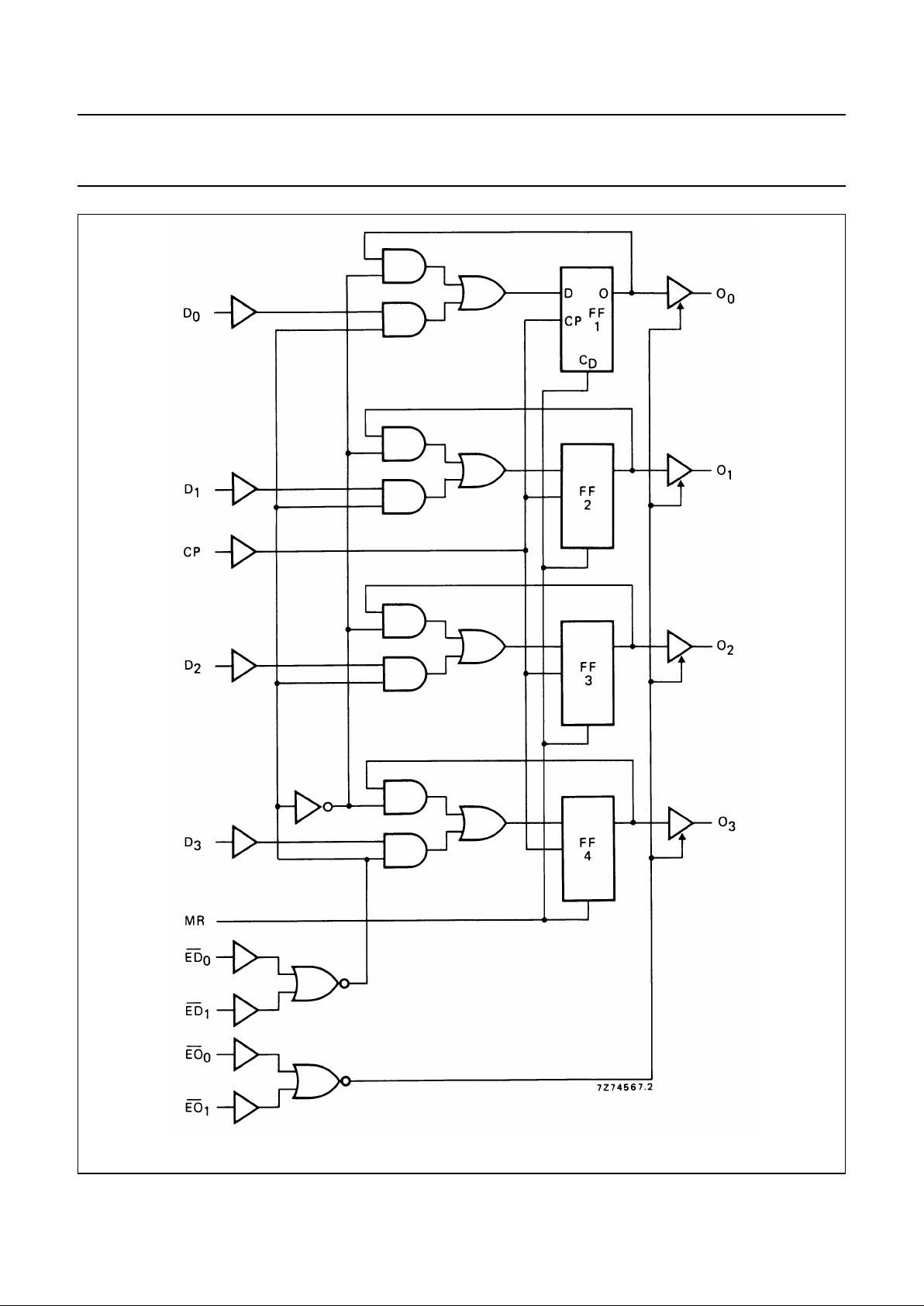
Fig.3 Logic diagram.
Page 4

January 1995 4
Philips Semiconductors Product specification
Quadruple D-type register with 3-state outputs
HEF4076B
MSI
FUNCTION TABLE
INPUTS OUTPUTS
MR CP ED
0
ED
1
D
n
O
n
HX XXX L
L H X X no change
L X H X no change
LLLHH
LLLLL
L X X X no change
Notes
1. EO0= EO1= LOW
When either EO0or EO1is HIGH, the outputs are
disabled (high impedance OFF-state).
H = HIGH state (the more positive voltage)
L = LOW state (the less positive voltage)
X = state is immaterial
= positive-going transition
= negative-going transition
AC CHARACTERISTICS
V
SS
= 0 V; T
amb
=25°C; CL= 50 pF; input transition times ≤ 20 ns; see also waveforms Fig.4
V
DD
V
SYMBOL MIN. TYP. MAX.
TYPICAL EXTRAPOLA TION
FORMULA
Propagation delays
CP → O
n
5 150 305 ns 123 ns + (0,55 ns/pF) C
L
HIGH to LOW 10 t
PHL
60 120 ns 49 ns + (0,23 ns/pF) C
L
15 45 85 ns 37 ns + (0,16 ns/pF) C
L
5 160 320 ns 133 ns + (0,55 ns/pF) C
L
LOW to HIGH 10 t
PLH
65 130 ns 54 ns + (0,23 ns/pF) C
L
15 45 90 ns 37 ns + (0,16 ns/pF) C
L
MR → O
n
5 95 190 ns 68 ns + (0,55 ns/pF) C
L
HIGH to LOW 10 t
PHL
40 85 ns 29 ns + (0,23 ns/pF) C
L
15 30 65 ns 22 ns + (0,16 ns/pF) C
L
Output transition times 5 60 120 ns 10 ns + (1,0 ns/pF) C
L
HIGH to LOW 10 t
THL
30 60 ns 9 ns + (0,42 ns/pF) C
L
15 20 40 ns 6 ns + (0,28 ns/pF) C
L
5 60 120 ns 10 ns + (1,0 ns/pF) C
L
LOW to HIGH 10 t
TLH
30 60 ns 9 ns + (0,42 ns/pF) C
L
15 20 40 ns 6 ns + (0,28 ns/pF) C
L
3-state propagation times
Output disable times 5 50 105 ns
EOn→ O
n
10 t
PHZ
35 70 ns
HIGH 15 30 65 ns
54590ns
LOW 10 t
PLZ
30 65 ns
15 30 60 ns
Page 5

January 1995 5
Philips Semiconductors Product specification
Quadruple D-type register with 3-state outputs
HEF4076B
MSI
AC CHARACTERISTICS
V
SS
= 0 V; T
amb
=25°C; CL= 50 pF; input transition times ≤ 20 ns
Output enable times 5 65 130 ns
EOn→ O
n
10 t
PZH
30 55 ns
HIGH 15 20 40 ns
5 60 120 ns
LOW 10 t
PZL
25 50 ns
15 20 35 ns
V
DD
V
SYMBOL MIN. TYP. MAX.
TYPICAL EXTRAPOLATION
FORMULA
Set-up times 5 10 −15 ns
see also waveforms
Fig.4
Dn→ CP 10 t
su
0 −10 ns
15 0 −5ns
50−50 ns
EDn→ CP 10 t
su
0 −20 ns
15 0 −15 ns
Hold times 5 55 30 ns
D
n
→ CP 10 t
hold
20 10 ns
15 15 10 ns
525−25 ns
EDn→ CP 10 t
hold
10 −10 ns
15 5 −5ns
Minimum clock 5 120 60 ns
pulse width; LOW 10 t
WCPL
45 20 ns
15 30 15 ns
Minimum MR pulse 5 55 25 ns
width; HIGH 10 t
WMRH
30 15 ns
15 20 10 ns
Recovery time 5 90 45 ns
for MR 10 t
RMR
35 15 ns
15 20 10 ns
Maximum clock 5 4 8 MHz
pulse frequency 10 f
max
11 22 MHz
15 16 32 MHz
V
DD
V
SYMBOL MIN. TYP. MAX.
TYPICAL EXTRAPOLA TION
FORMULA
Page 6

January 1995 6
Philips Semiconductors Product specification
Quadruple D-type register with 3-state outputs
HEF4076B
MSI
V
DD
V
TYPICAL FORMULA FOR P (µW)
Dynamic power 5 2200 f
i
+∑(foCL) × V
DD
2
where
dissipation per 10 9300 f
i
+∑(foCL) × V
DD
2
fi= input freq. (MHz)
package (P) 15 24 500 f
i
+∑(foCL) × V
DD
2
fo= output freq. (MHz)
C
L
= load capacitance (pF)
∑ (f
oCL
) = sum of outputs
V
DD
= supply voltage (V)
Page 7

January 1995 7
Philips Semiconductors Product specification
Quadruple D-type register with 3-state
outputs
HEF4076B
MSI
This text is here in white to force landscape pages to be rotated correctly when browsing through the pdf in the Acrobat reader.This text is here in
_white to force landscape pages to be rotated correctly when browsing through the pdf in the Acrobat reader.This text is here inThis text is here in
white to force landscape pages to be rotated correctly when browsing through the pdf in the Acrobat reader. white to force landscape pages to be ...
Fig.4 Waveforms showing propagation delays, output disable/enable times, minimum CP and MR pulse widths, set-up and hold times for
Dnto CP and EDnto CP, and recovery time for MR. Set-up and hold times are shown as positive values but may be specified as
negative values.
 Loading...