

Page 1
INTEGRATED CIRCUITS
DATA SH EET
For a complete data sheet, please also download:
•The IC04 LOCMOS HE4000B Logic
Family Specifications HEF, HEC
•The IC04 LOCMOS HE4000B Logic
Package Outlines/Information HEF, HEC
HEF4050B
buffers
HEX non-inverting buffers
Product specification
File under Integrated Circuits, IC04
January 1995
Page 2
Philips Semiconductors Product specification
HEX non-inverting buffers
DESCRIPTION
The HEF4050B provides six non-inverting buffers with
high current output capability suitable for driving TTL or
high capacitive loads. Since input voltages in excess of the
buffers’ supply voltage are permitted, the buffers may also
be used to convert logic levels of up to 15 V to standard
TTL levels. Their guaranteed fan-out into common bipolar
logic elements is shown in the table below.
HEF4050B
buffers
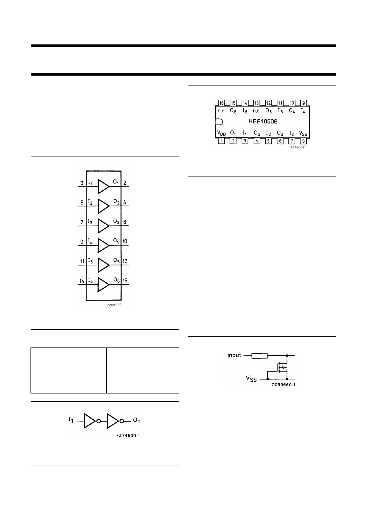
Fig.2 Pinning diagram.
HEF4050BP(N): 16-lead DIL; plastic
(SOT38-1)
HEF4050BD(F): 16-lead DIL; ceramic (cerdip)
(SOT74)
HEF4050BT(D): 16-lead SO; plastic
(SOT109-1)
( ): Package Designator North America
Fig.1 Functional diagram.
Guaranteed fan-out in common logic families
DRIVEN ELEMENT
standard TTL 2
74 LS 9
74 L 16
GUARANTEED
FAN-OUT
APPLICATION INFORMATION
Some examples of applications for the HEF4050B are:
• LOCMOS to DTL/TTL converter
• HIGH sink current for driving 2 TTL loads
• HIGH-to-LOW level logic conversion
Input protection
Fig.4 Input protection circuit that allows input
voltages in excess of VDD.
FAMILY DATA, IDDLIMITS category BUFFERS
See Family Specifications
Fig.3 Logic diagram (one gate).
January 1995 2
Page 3
Philips Semiconductors Product specification
HEX non-inverting buffers
HEF4050B
buffers
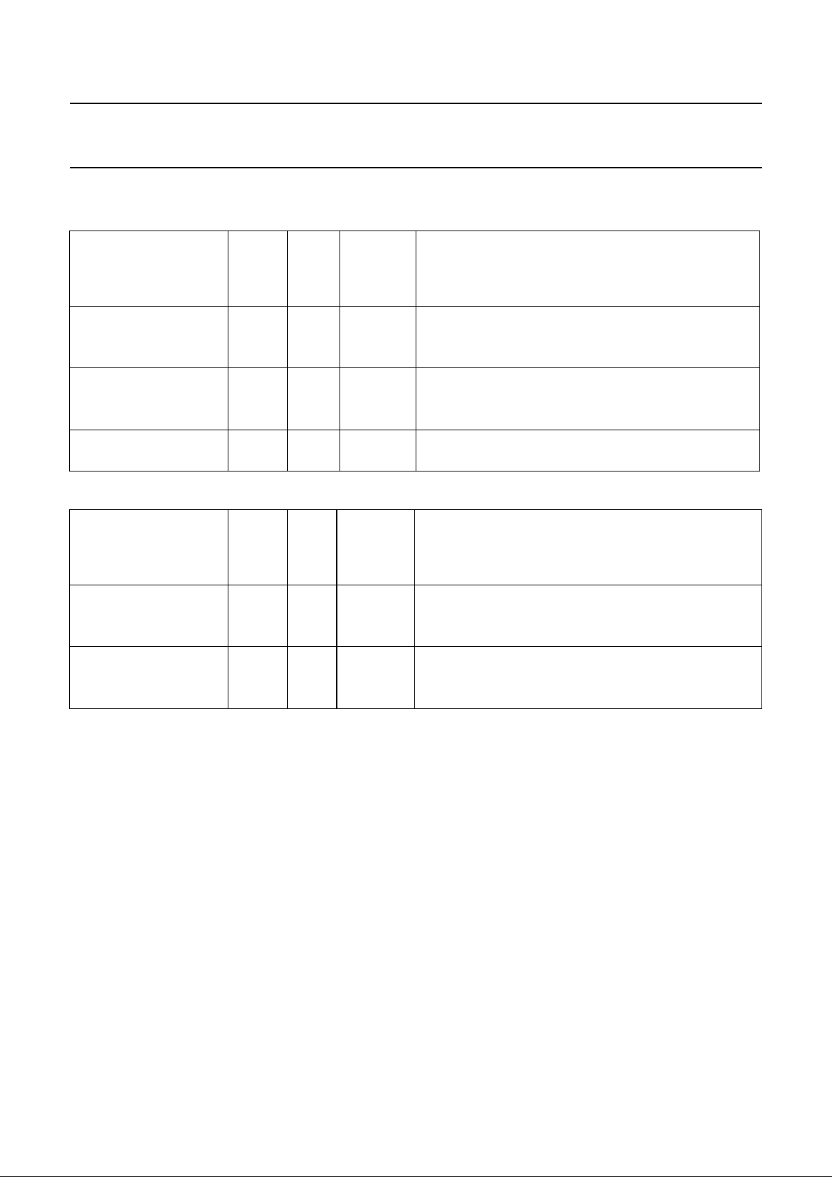
DC CHARACTERISTICS
V
= 0 V; VI=VSSor V
SS
HEF
Output (sink) 4,75 0,4 3,5 − 2,9 − 2,3 − mA
current LOW 10 0,5 I
Output (source) 5 4,6 0,52 − 0,44 − 0,36 − mA
current HIGH 10 9,5 I
Output (source)
current HIGH 5 2,5 I
HEC
DD
T
(°C)
V
DD
V
V
O
SYMBOL
V
−40 +25 +85
amb
MIN. MAX. MIN. MAX. MIN. MAX.
OL
12,0 − 10,0 − 8,0 − mA
15 1,5 24,0 − 20,0 − 16,0 − mA
OH
1,3 − 1,1 − 0,9 − mA
15 13,5 3,6 − 3,0 − 2,4 − mA
OH
V
DD
V
V
O
SYMBOL
V
1,7 − 1,4 − 1,1 − mA
T
(°C)
amb
−55 +25 +125
MIN. MAX. MIN. MAX. MIN. MAX.
Output (sink) 4,75 0,4 3,6 − 2,9 − 1,9 − mA
current LOW 10 0,5 I
OL
12,5 − 10,0 − 6,7 − mA
15 1,5 25,0 − 20,0 − 13,0 − mA
Output (source) 5 4,6 0,52 − 0,44 − 0,36 − mA
current HIGH 10 9,5 I
OH
1,3 − 1,1 − 0,9 − mA
15 13,5 3,6 − 3,0 − 2,4 − mA
January 1995 3
Page 4
Philips Semiconductors Product specification
HEX non-inverting buffers
HEF4050B
buffers
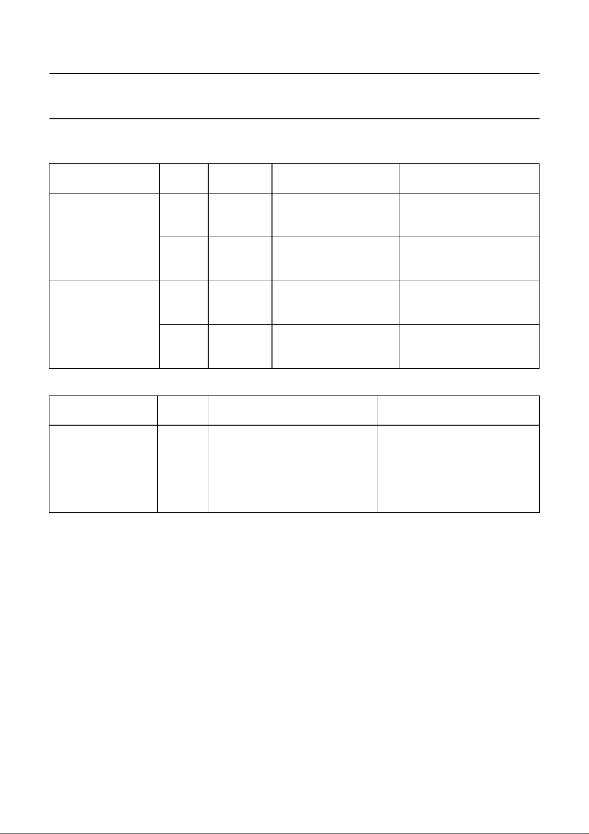
AC CHARACTERISTICS
V
= 0 V; T
SS
Propagation delays 5 35 70 ns 26 ns + (0,18 ns/pF) C
I
n
HIGH to LOW 15 15 30 ns 12 ns + (0,05 ns/pF) C
LOW to HIGH 10 t
Output transition 5 25 50 ns 7 ns + (0,35 ns/pF) C
times 10 t
HIGH to LOW 15 7 14 ns 2 ns + (0,09 ns/pF) C
LOW to HIGH 10 t
=25°C; CL= 50 pF; input transition times ≤ 20 ns
amb
V
DD
V
O
n
10 t
SYMBOL TYP. MAX.
PHL
5 55 110 ns 28 ns + (0,55 ns/pF) C
PLH
15 20 40 ns 12 ns + (0,16 ns/pF) C
THL
5 60 120 ns 10 ns + (1,0 ns/pF) C
TLH
15 20 40 ns 6 ns + (0,28 ns/pF) C
TYPICAL EXTRAPOLATION
FORMULA
20 35 ns 16 ns + (0,08 ns/pF) C
25 55 ns 14 ns + (0,23 ns/pF) C
10 20 ns 3 ns + (0,14 ns/pF) C
30 60 ns 9 ns + (0,42 ns/pF) C
L
L
L
L
L
L
L
L
L
L
L
L
V
DD
V
TYPICAL FORMULA FOR P (µW)
Dynamic power 5 3 800 f
dissipation per 10 11 600 f
package (P) 15 65 900 f
+∑(foCL) × V
i
+∑(foCL) × V
i
+∑(foCL) × V
i
DD
DD
DD
2
2
2
where
fi= input freq. (MHz)
fo= output freq. (MHz)
C
= load capacitance (pF)
L
∑ (f
) = sum of outputs
oCL
= supply voltage (V)
V
DD
January 1995 4
 Loading...