

Page 1

INTEGRATED CIRCUITS
DATA SH EET
For a complete data sheet, please also download:
•The IC04 LOCMOS HE4000B Logic
Family Specifications HEF, HEC
•The IC04 LOCMOS HE4000B Logic
Package Outlines/Information HEF, HEC
HEF4043B
MSI
Quadruple R/S latch with 3-state
outputs
Product specification
File under Integrated Circuits, IC04
January 1995
Page 2
Philips Semiconductors Product specification
Quadruple R/S latch with 3-state outputs
DESCRIPTION
The HEF4043B is a quadruple R/S latch with 3-state
outputs with a common output enable input (EO). Each
latch has an active HIGH set input (S0 to S3), an active
HIGH reset input (R0to R3) and an active HIGH 3-state
output (O0to O3).
When EO is HIGH, the state of the latch output (On) can be
determined from the function table below. When EO is
LOW, the latch outputs are in the high impedance
OFF-state. EO does not affect the state of the latch.
The high impedance off-state feature allows common
busing of the outputs.
HEF4043B
MSI
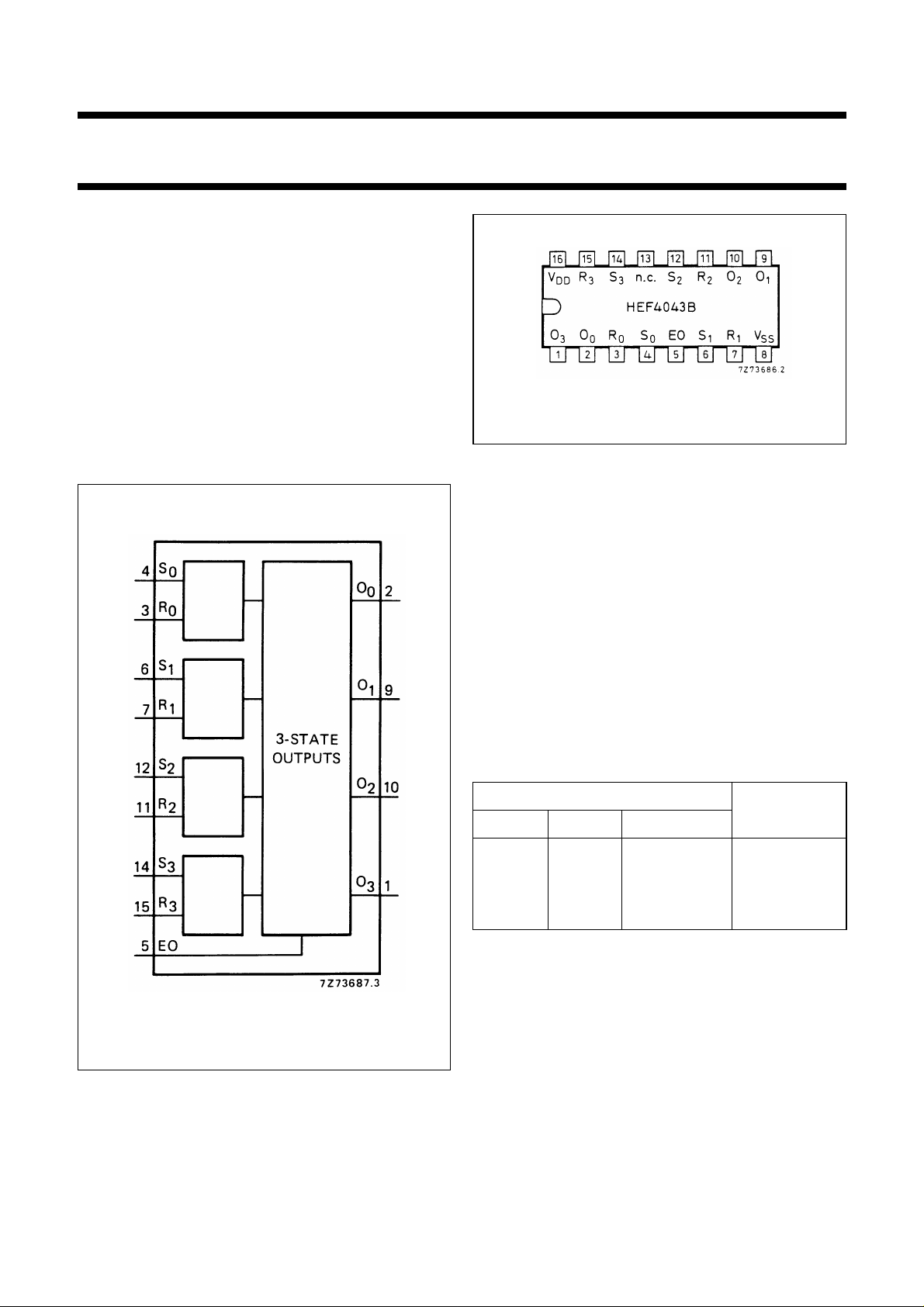
Fig.2 Pinning diagram.
HEF4043BP(N): 16-lead DIL; plastic (SOT38-1)
HEF4043BD(F): 16-lead DIL; ceramic (cerdip) (SOT74)
HEF4043BT(D): 16-lead SO; plastic (SOT109-1)
( ): Package Designator North America
Fig.1 Functional diagram.
PINNING
EO common output enable input
S
R
O
to S
0
to R
0
0
to O
3
3
3
set inputs (active HIGH)
reset inputs (active HIGH)
3-state buffered latch outputs
FUNCTION TABLE
INPUTS OUTPUT
EO S
n
R
n
O
LX X Z
HL H L
HH X H
H L L latched
Notes
1. H = HIGH state (the more positive voltage)
L = LOW state (the less positive voltage)
X = state immaterial
Z = high impedance state
n
January 1995 2
FAMILY DATA, IDDLIMITS category MSI
See Family Specifications
Page 3
Philips Semiconductors Product specification
Quadruple R/S latch with 3-state outputs
HEF4043B
MSI
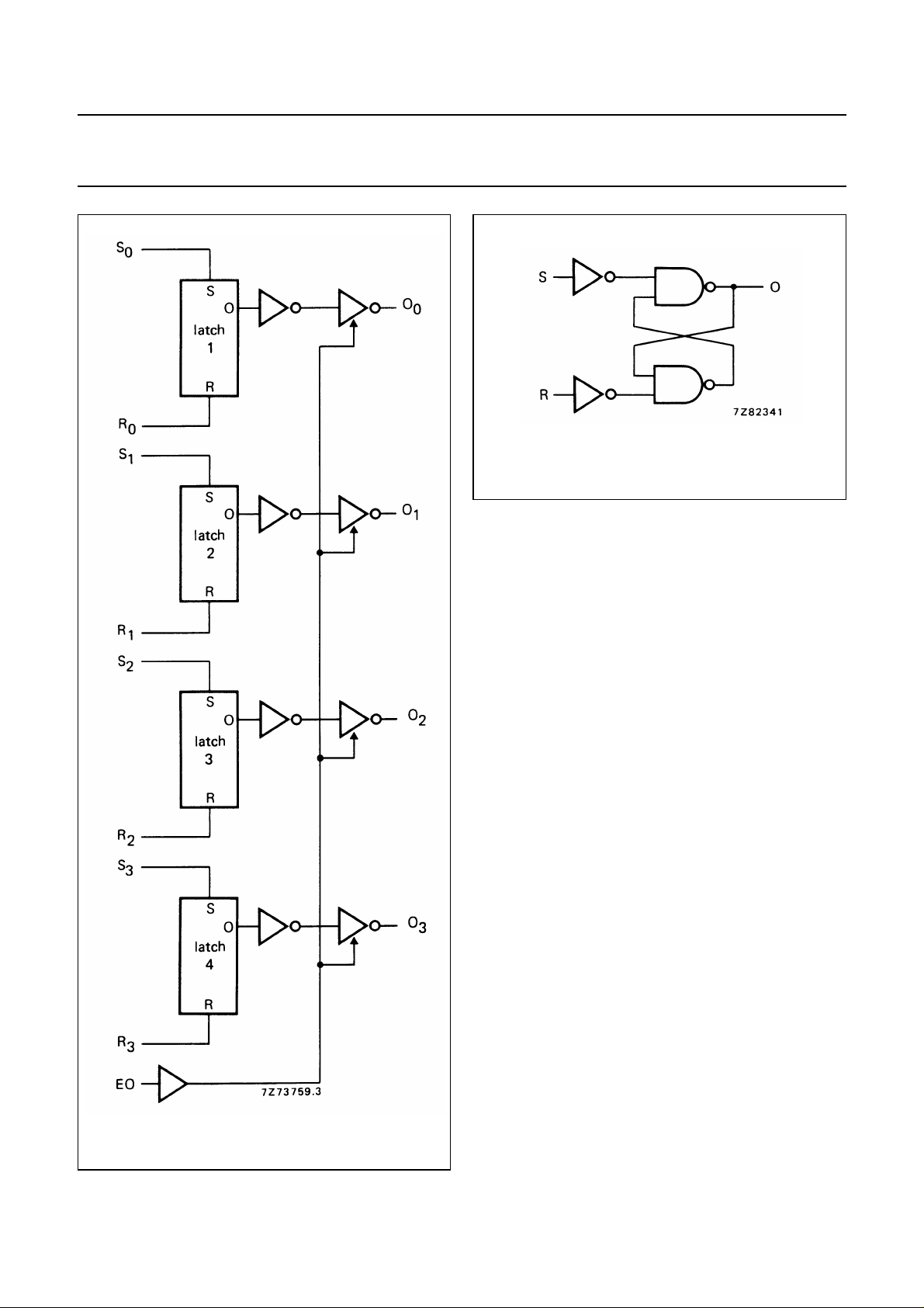
Fig.4 Logic diagram (one latch).
Fig.3 Logic diagram.
January 1995 3
Page 4
Philips Semiconductors Product specification
Quadruple R/S latch with 3-state outputs
HEF4043B
MSI
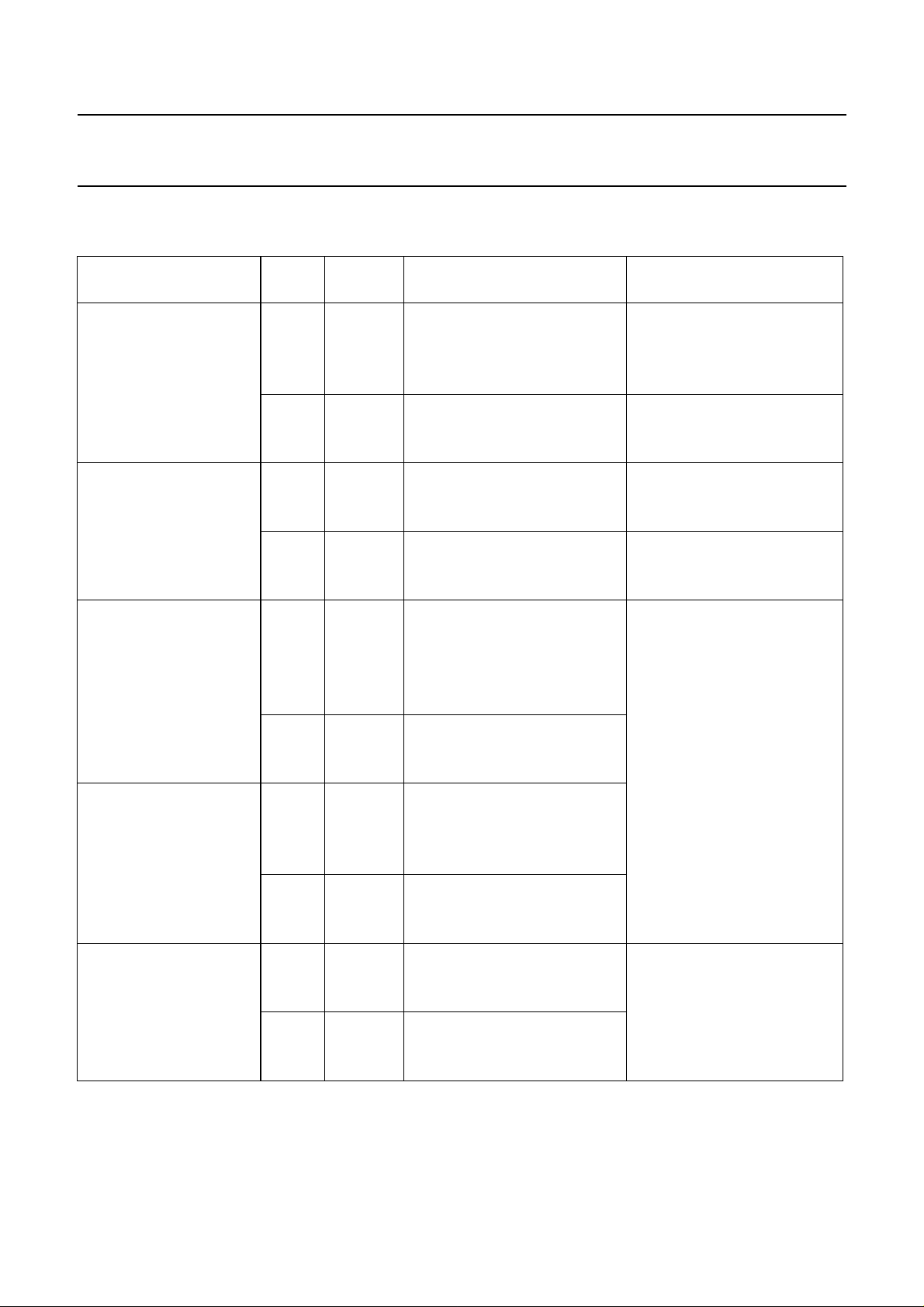
AC CHARACTERISTICS
V
= 0 V; T
SS
Propagation delays
Rn→ O
HIGH to LOW 10 t
Sn→ O
LOW to HIGH 10 t
Output transition 5 60 120 ns 10 ns + (1,0 ns/pF) C
times 10 t
HIGH to LOW 15 20 40 ns 6 ns + (0,28 ns/pF) C
LOW to HIGH 10 t
3-state propagation delays
Output disable times
EO → O
HIGH 10 t
LOW 10 t
Output enable times
EO → O
HIGH 10 t
LOW 10 t
Minimum S
pulse width; HIGH 10 t
Minimum R
pulse width; HIGH 10 t
=25°C; CL= 50 pF; input transition times ≤ 20 ns
amb
V
DD
SYMBOL MIN. TYP. MAX.
V
n
5 90 180 ns 63 ns + (0,55 ns/pF) C
PHL
15 25 50 ns 17 ns + (0,16 ns/pF) C
n
5 65 135 ns 38 ns + (0,55 ns/pF) C
PLH
15 15 35 ns 7 ns + (0,16 ns/pF) C
THL
5 60 120 ns 10 ns + (1,0 ns/pF) C
TLH
15 20 40 ns 6 ns + (0,28 ns/pF) C
n
54590ns
PHZ
15 10 25 ns
5 50 100 ns
PLZ
15 10 25 ns
n
52550ns
PZH
15 10 25 ns
54080ns
PZL
15 15 35 ns
n
53015 ns
WSH
20 10 ns
15 16 8 ns
n
53015 ns
WRH
20 10 ns
15 16 8 ns
TYPICAL EXTRAPOLATION
FORMULA
35 70 ns 24 ns + (0,23 ns/pF) C
25 50 ns 14 ns + (0,23 ns/pF) C
30 60 ns 9 ns + (0,42 ns/pF) C
30 60 ns 9 ns + (0,42 ns/pF) C
20 35 ns
20 40 ns
15 30 ns
20 45 ns
see also waveforms
Fig.5
L
L
L
L
L
L
L
L
L
L
L
L
January 1995 4
Page 5
Philips Semiconductors Product specification
Quadruple R/S latch with 3-state outputs
V
DD
V
Dynamic power 5 1100 f
dissipation per 10 4400 f
package (P) 15 11 400 f
TYPICAL FORMULA FOR P (µW)
+∑(foCL) × V
i
+ ∑(foCL) × V
i
+∑(foCL) × V
i
DD
DD
DD
HEF4043B
MSI
2
2
2
where
fi= input freq. (MHz)
fo= output freq. (MHz)
C
= load capacitance (pF)
L
∑(f
) = sum of outputs
oCL
= supply voltage (V)
V
DD
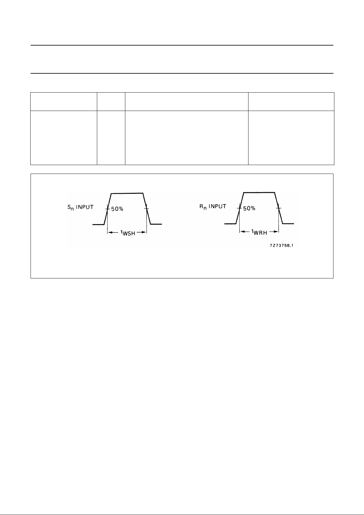
Fig.5 Waveforms showing minimum Snand Rnpulse widths.
APPLICATION INFORMATION
An example of application for the HEF4043B is:
• Four-bit storage with output enable
January 1995 5
 Loading...