

Page 1

DATA SH EET
Product specification
File under Integrated Circuits, IC04
January 1995
INTEGRATED CIRCUITS
HEF4041B
buffers
Quadruple true/complement buffer
For a complete data sheet, please also download:
•The IC04 LOCMOS HE4000B Logic
Family Specifications HEF, HEC
•The IC04 LOCMOS HE4000B Logic
Package Outlines/Information HEF, HEC
Page 2
January 1995 2
Philips Semiconductors Product specification
Quadruple true/complement buffer
HEF4041B
buffers
DESCRIPTION
The HEF4041B is a quadruple true/complement buffer
which provides both an inverted active LOW output
(O) and a non-inverted active HIGH output (O) for each
input (I).
The buffers exhibit high current output capability suitable
for driving TTL or high capacitive loads.
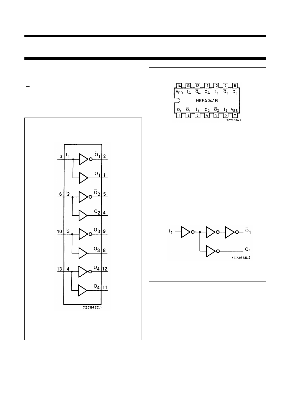
Fig.1 Functional diagram.
APPLICATION INFORMATION
Some examples of applications for the HEF4041B are:
• LOCMOS to DTL/TTL converter
• High current sink and source driver
FAMILY DATA, I
DD
LIMITS category BUFFERS
See Family Specifications
HEF4041BP(N): 14-lead DIL; plastic
(SOT27-1)
HEF4041BD(F): 14-lead DIL; ceramic (cerdip)
(SOT73)
HEF4041BT(D): 14-lead SO; plastic
(SOT108-1)
( ): Package Designator North America
Fig.2 Pinning diagram.
Fig.3 Logic diagram (one buffer).
Page 3

January 1995 3
Philips Semiconductors Product specification
Quadruple true/complement buffer
HEF4041B
buffers
DC CHARACTERISTICS
V
SS
= 0 V; VI=VSSor V
DD
AC CHARACTERISTICS
V
SS
= 0 V; T
amb
=25°C; CL= 50 pF; input transition times ≤ 20 ns
V
DD
V
V
OH
V
V
OL
V
SYMBOL
T
amb
(°C)
−40 +25 +85
MIN. MAX. MIN. TYP. MIN. MAX.
Output (source) current 5 4,6 1,6 1,3 2,6 1,0 mA
HIGH 10 9,5 −I
OH
4,5 3,6 7,0 2,7 mA
15 13,5 16,0 14,0 30,0 10,0 mA
HIGH 5 2,5 −I
OH
5,0 4,0 8,0 3,0 mA
Output (sink) current 4,75 0,4 2,0 1,7 4,0 1,35 mA
LOW 10 0,5 I
OL
7,5 6,0 12,0 4,5 mA
15 1,5 23,0 20,0 35,0 15,0 mA
V
DD
V
SYMBOL MIN. TYP. MAX.
TYPICAL EXTRAPOLATION
FORMULA
Propagation delays
In→ O
n
53065ns17ns+(0,27 ns/pF) C
L
HIGH to LOW 10 t
PHL
20 40 ns 14 ns + (0,11 ns/pF) C
L
15 15 30 ns 12 ns + (0,08 ns/pF) C
L
53055ns17ns+(0,27 ns/pF) C
L
LOW to HIGH 10 t
PLH
15 30 ns 9 ns + (0,11 ns/pF) C
L
15 10 20 ns 7 ns + (0,08 ns/pF) C
L
In→ O
n
53575ns22ns+(0,27 ns/pF) C
L
HIGH to LOW 10 t
PHL
20 40 ns 14 ns + (0,11 ns/pF) C
L
15 15 30 ns 12 ns + (0,08 ns/pF) C
L
53575ns22ns+(0,27 ns/pF) C
L
LOW to HIGH 10 t
PLH
20 40 ns 14 ns + (0,11 ns/pF) C
L
15 15 30 ns 12 ns + (0,08 ns/pF) C
L
Output transition times 5 25 50 ns 5 ns + (0,40 ns/pF) C
L
On→ O
n
10 t
THL
12 25 ns 2 ns + (0,21 ns/pF) C
L
HIGH to LOW 15 8 20 ns 1 ns + (0,14 ns/pF) C
L
52545ns5ns+(0,40 ns/pF) C
L
LOW to HIGH 10 t
TLH
12 25 ns 2 ns + (0,21 ns/pF) C
L
15 8 20 ns 1 ns + (0,14 ns/pF) C
L
Page 4

January 1995 4
Philips Semiconductors Product specification
Quadruple true/complement buffer
HEF4041B
buffers
V
DD
V
TYPICAL FORMULA FOR P (µW)
Dynamic power 5 3100 f
i
+∑(foCL) × V
DD
2
where
dissipation per 10 12 700 f
i
+∑(foCL) × V
DD
2
fi= input freq. (MHz)
package (P) 15 33 800 f
i
+∑(foCL) × V
DD
2
fo= output freq. (MHz)
C
L
= load capacitance (pF)
∑ (f
oCL
) = sum of outputs
V
DD
= supply voltage (V)
 Loading...