

Datasheet HEF40374BU, HEF40374BT, HEF40374BPB, HEF40374BP, HEF40374BDB Datasheet (Philips)
...Page 1
DATA SH EET
Product specification
File under Integrated Circuits, IC04
January 1995
INTEGRATED CIRCUITS
HEF40374B
MSI
Octal D-type flip-flop with 3-state
outputs
For a complete data sheet, please also download:
•The IC04 LOCMOS HE4000B Logic
Family Specifications HEF, HEC
•The IC04 LOCMOS HE4000B Logic
Package Outlines/Information HEF, HEC
Page 2
January 1995 2
Philips Semiconductors Product specification
Octal D-type flip-flop with 3-state outputs
HEF40374B
MSI
DESCRIPTION
The HEF40374B is an octal D-type flip-flop with 3-state
buffered outputs with a common clock input (CP). The
device is used primarily as an 8-bit positive edge-triggered
storage register for interfacing with a 3-state bus. Data on
the D-inputs is transferred to storage during the
LOW-to-HIGH transition of the clock (CP) input. The
3-state output buffers are controlled by an active LOW
output enable input (EO). A HIGH on EO forces the eight
outputs to a high impedance OFF-state. When EO is
LOW, the data in the register appears at the outputs.
The output stages have high current output capability
suitable for driving highly capacitive loads.
The device features hysteresis on the CP input to improve
noise rejection.
Schmitt-trigger action in the E input makes the circuit
highly tolerant to slower input rise and fall times.
The HEF40374B is pin and functionally compatible with
the TTL ‘374’ device.
Supply voltage range: 3 to 15 V.
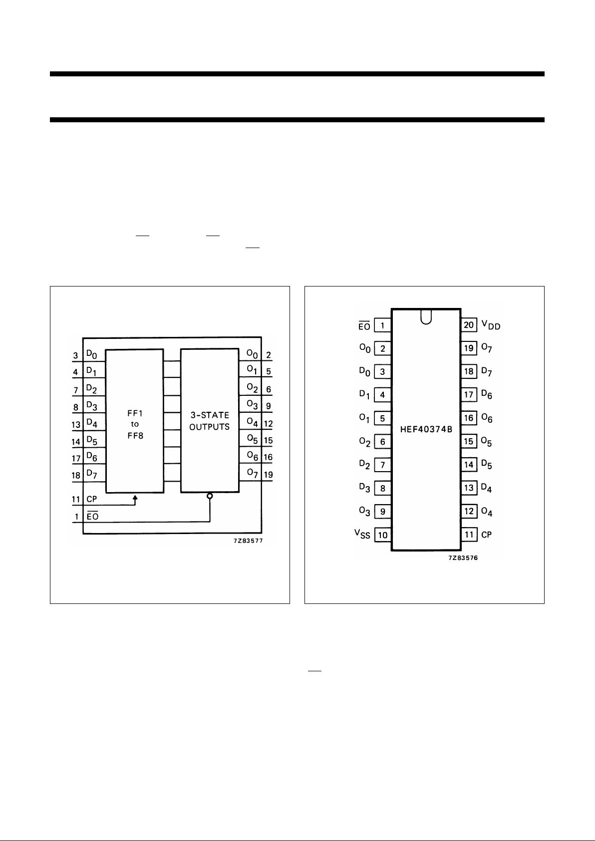
Fig.1 Functional diagram. Fig.2 Pinning diagram.
HEF40374BP(N): 20-lead DIL; plastic (SOT146-1)
HEF40374BD(F): 20-lead DIL; ceramic (cerdip)
(SOT152)
HEF40374BT(D): 20-lead SO; plastic (SOT163-1)
( ): Package Designator North America
PINNING
FAMILY DATA, I
DD
LIMITS category MSI
See Family Specifications
D
0
to D
7
data inputs
CP clock input
EO output enable input (active LOW)
O
0
to O
7
3-state buffered outputs
Page 3
January 1995 3
Philips Semiconductors Product specification
Octal D-type flip-flop with 3-state outputs
HEF40374B
MSI
This text is here in white to force landscape pages to be rotated correctly when browsing through the pdf in the Acrobat reader.This text is here in
_white to force landscape pages to be rotated correctly when browsing through the pdf in the Acrobat reader.This text is here inThis text is here in
white to force landscape pages to be rotated correctly when browsing through the pdf in the Acrobat reader. white to force landscape pages to be ...
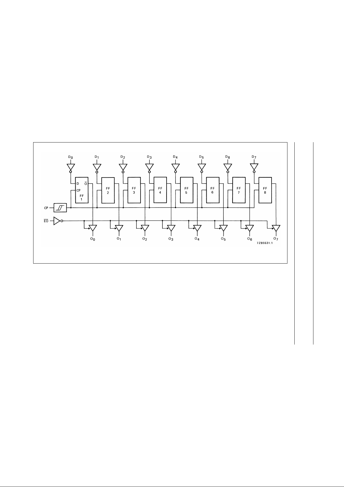
Fig.3 Logic diagram.
Page 4
January 1995 4
Philips Semiconductors Product specification
Octal D-type flip-flop with 3-state outputs
HEF40374B
MSI
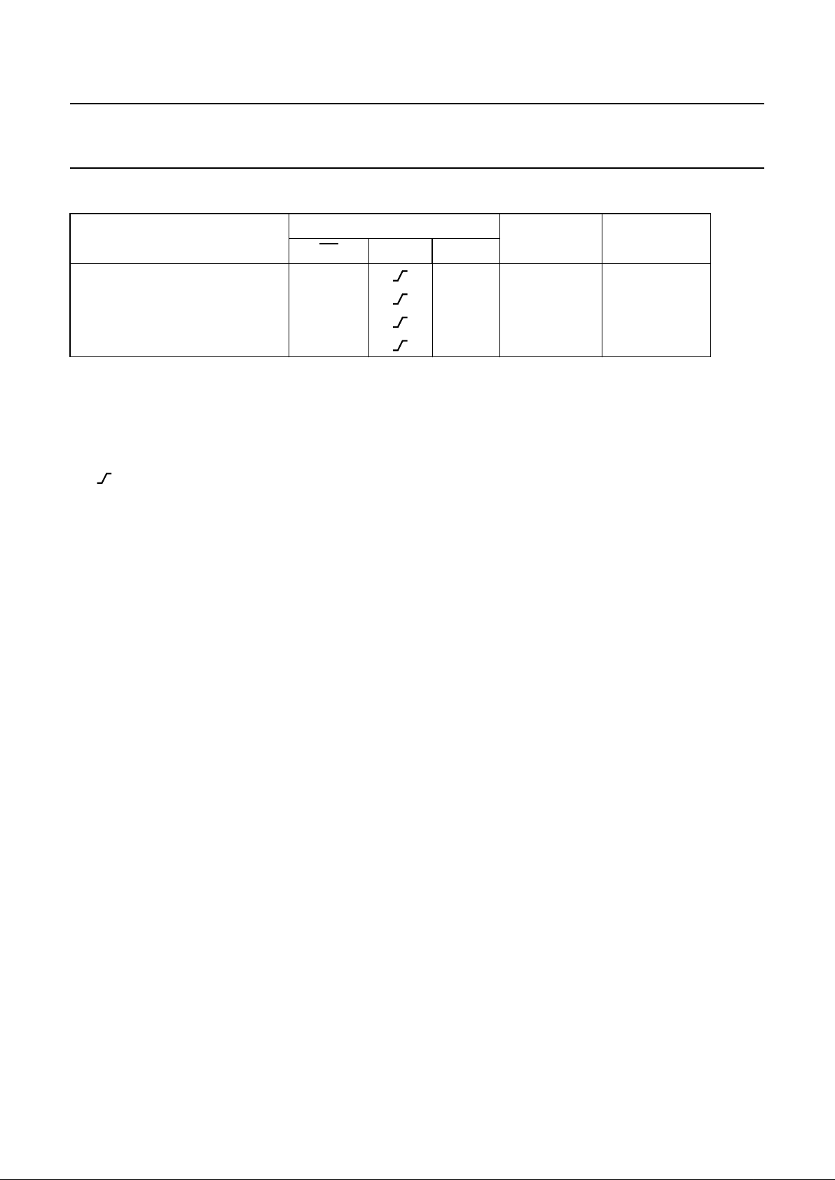
FUNCTION TABLE
Notes
1. H =HIGH state (the more positive voltage)
h = HIGH state (one set-up time prior to the LOW-to-HIGH clock transition)
L = LOW state (the less positive voltage)
I = LOW state (one set-up time prior to the LOW-to-HIGH clock transition)
Z = high impedance OFF-state
= LOW-to-HIGH clock transition
OPERATING MODES
INPUTS INTERNAL
REGISTER
OUTPUTS
O0TO O
7
EO CP D
n
load & read register
LILL
LhHH
load register & disable outputs
HILZ
HhHZ
Page 5
January 1995 5
Philips Semiconductors Product specification
Octal D-type flip-flop with 3-state outputs
HEF40374B
MSI
RATINGS
Limiting values in accordance with the Absolute Maximum System (IEC 134)
See Family Specifications, except for:
DC CHARACTERISTICS
V
SS
=0 V
D.C. current into any input ± I
I
max. 10 mA
D.C. source or sink current into any output ± I
O
max. 25 mA
D.C. current into the supply terminals ± I max. 100 mA
V
DD
V
V
OH
V
V
OL
V
SYMBOL
T
amb
(°C)
−40 + 25 + 85
MIN. TYP. MIN. TYP. MIN. TYP.
Output current 5 4,6 0,75 0,6 1,2 0,45 mA
HIGH 10 9,5 −I
OH
1,85 1,5 3,0 1,1 mA
15 13,5 14,5 15 50 15,5 mA
Output current 5 3,6 9,3 10 24 10,7 mA
HIGH 10 8,4 −I
OH
14,4 15 46 15,0 mA
15 13,2 19,5 20 62 19,8 mA
Output current 5 0,4 2,9 2,3 5,4 1,75 mA
LOW 10 0,5 I
OL
9,5 7,6 17 5,50 mA
15 1,5 30,0 25 45 19,0 mA
Hysteresis 5 220 mV
voltage at 10 V
H
250 mV
clock input (CP) 15 320 mV
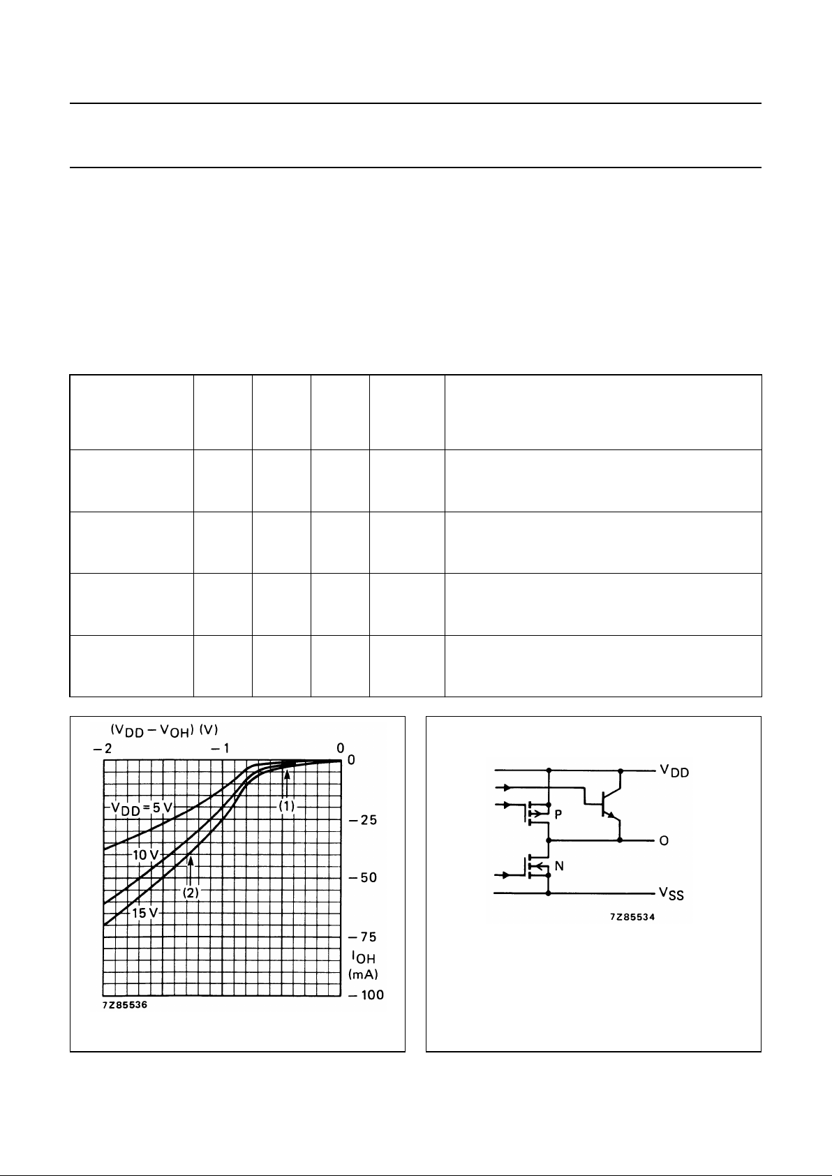
Fig.4 Typical output source current characteristic. Fig.5 Schematic diagram of output stage.
(1) P-channel MOS transistor conducting.
(2) P-channel MOS transistor and bipolar
n-p-n transistor conducting.
Page 6
January 1995 6
Philips Semiconductors Product specification
Octal D-type flip-flop with 3-state outputs
HEF40374B
MSI
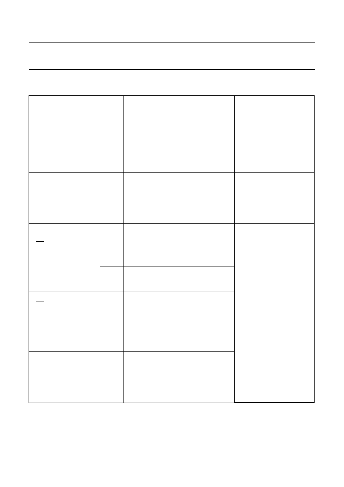
AC CHARACTERISTICS
V
SS
= 0 V; T
amb
=25°C; CL= 50 pF; input transition times ≤ 20 ns
V
DD
V
SYMBOL MIN. TYP. MAX.
TYPICAL EXTRAPOLATION
FORMULA
Propagation delays
CP → O
n
5 125 250 ns 113 ns + (0,24 ns/pF) C
L
HIGH to LOW 10 t
PHL
55 110 ns 54 ns + (0,01 ns/pF) C
L
15 40 80 ns 36 ns + (0,07 ns/pF) C
L
CP → O
n
5 125 250 ns 122 ns + (0,06 ns/pF) C
L
LOW to HIGH 10 t
PLH
55 110 ns 53 ns + (0,03 ns/pF) C
L
15 40 80 ns 39 ns + (0,02 ns/pF) C
L
Output transition 5 40 80 ns
see Fig.6
times 10 t
THL
20 40 ns
HIGH to LOW 15 15 30 ns
53060ns
LOW to HIGH 10 t
TLH
20 40 ns
15 15 30 ns
3-state propagation delays
Output disable times
EO → O
n
5 60 120 ns
HIGH 10 t
PHZ
30 60 ns
15 24 48 ns
5 70 140 ns
LOW 10 t
PLZ
35 70 ns
15 30 60 ns
Output enable times
EO → O
n
5 65 130 ns
HIGH 10 t
PZH
30 60 ns
15 24 48 ns
5 85 170 ns
LOW 10 t
PZL
35 70 ns
15 25 50 ns
Set-up time 5 20 0 ns
D
n
→ CP 10 t
su
20 2 ns
15 20 5 ns
Hold time 5 20 10 ns
D
n
→ CP 10 t
hold
15 2 ns
15 10 0 ns
Page 7
January 1995 7
Philips Semiconductors Product specification
Octal D-type flip-flop with 3-state outputs
HEF40374B
MSI
AC CHARACTERISTICS
V
SS
= 0 V; T
amb
=25°C; input transition times ≤ 20 ns
Minimum clock 5 50 25 ns
pulse width; LOW 10 t
WCPL
25 12 ns
15 20 10 ns
Maximum clock 5 25 5 MHz
pulse frequency 10 f
max
6 12 MHz
15 8 17 MHz
V
DD
V
TYPICAL FORMULA FOR P (µW)
Dynamic power 5 3 775 f
i
+∑(foCL) × V
DD
2
where
dissipation per 10 15 700 f
i
+∑(foCL) × V
DD
2
fi= input freq. (MHz)
package (P) 15 40 575 f
i
+∑(foCL) × V
DD
2
fo= output freq. (MHz)
C
L
= load capacitance (pF)
∑ (f
oCL
) = sum of outputs
V
DD
= supply voltage (V)
V
DD
V
SYMBOL MIN. TYP. MAX.
TYPICAL EXTRAPOLATION
FORMULA
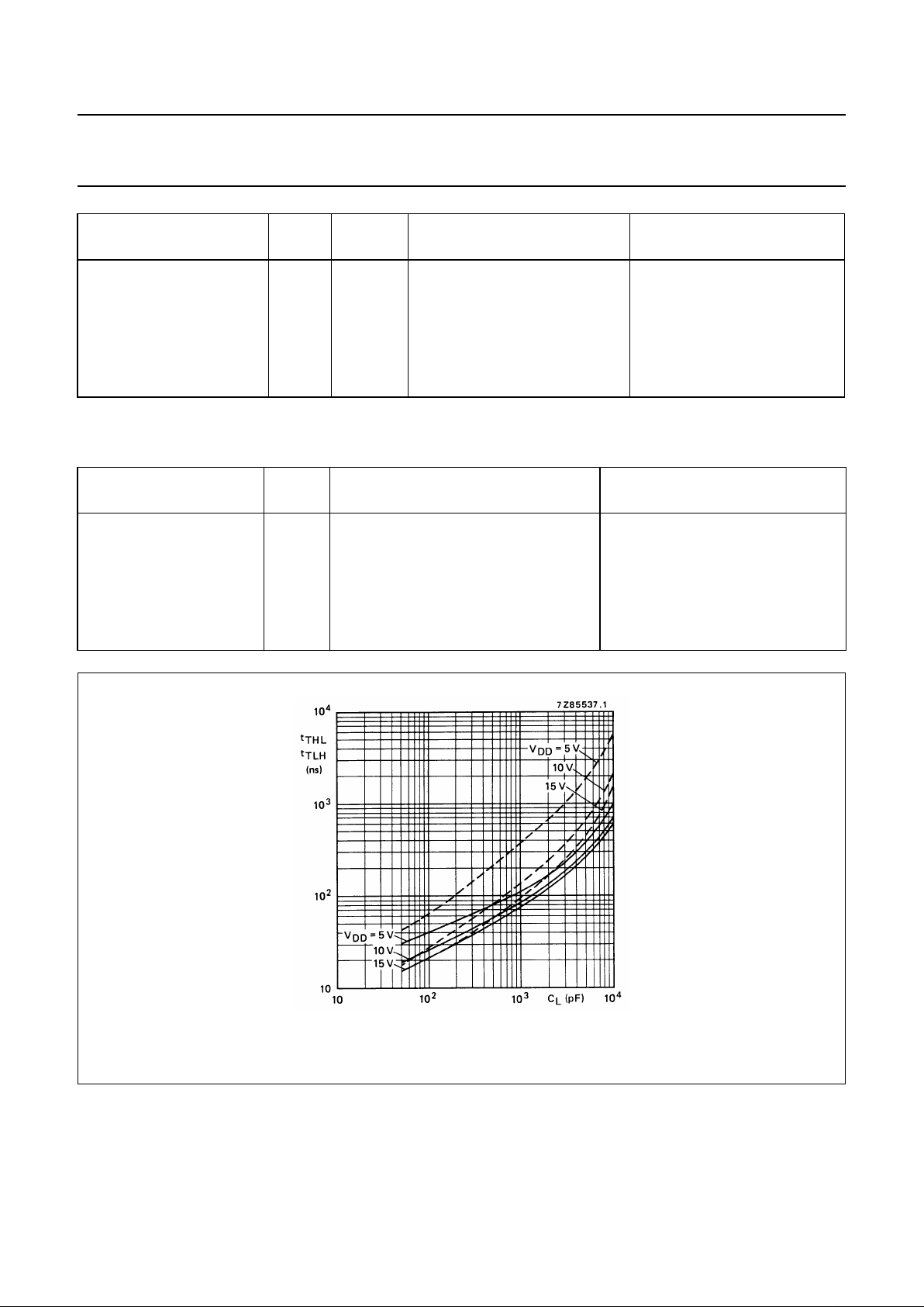
Fig.6 Output transition times as a function of the load capacitance. .
t
TLH
−−−− t
THL
 Loading...