

Page 1

DATA SH EET
Product specification
File under Integrated Circuits, IC04
January 1995
INTEGRATED CIRCUITS
HEF4030B
gates
Quadruple exclusive-OR gate
For a complete data sheet, please also download:
•The IC04 LOCMOS HE4000B Logic
Family Specifications HEF, HEC
•The IC04 LOCMOS HE4000B Logic
Package Outlines/Information HEF, HEC
Page 2
January 1995 2
Philips Semiconductors Product specification
Quadruple exclusive-OR gate
HEF4030B
gates
DESCRIPTION
The HEF4030B provides the positive quadruple
exclusive-OR function. The outputs are fully buffered for
highest noise immunity and pattern insensitivity of output
impedance.
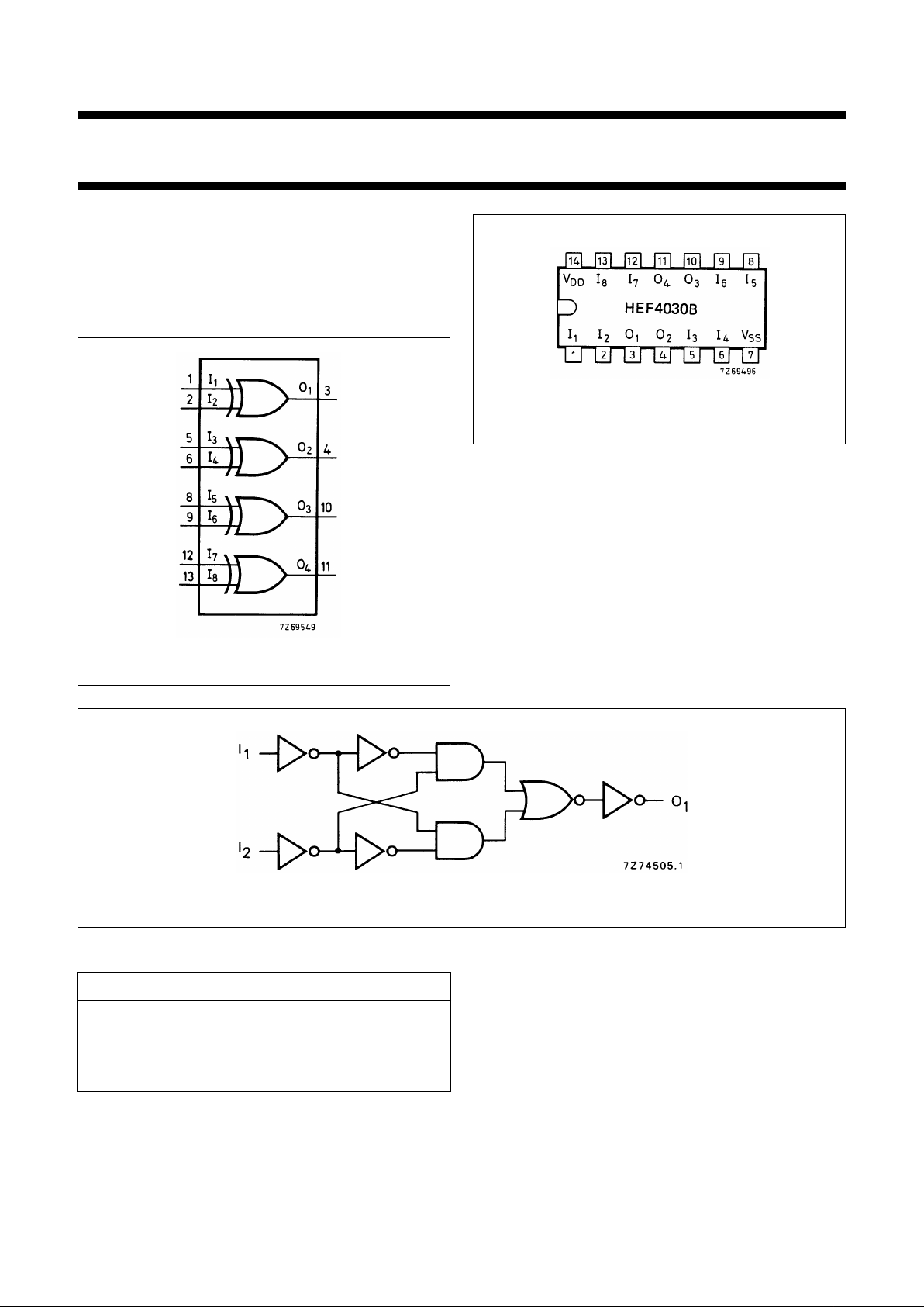
Fig.1 Functional diagram.
HEF4030BP(N): 14-lead DIL; plastic
(SOT27-1)
HEF4030BD(F): 14-lead DIL; ceramic (cerdip)
(SOT73)
HEF4030BT(D): 14-lead SO; plastic
(SOT108-1)
( ): Package Designator North America
Fig.2 Pinning diagram.
Fig.2 Logic diagram (one gate).
TRUTH TABLE
Notes
1. H = HIGH state (the more positive voltage)
L = LOW state (the less positive voltage)
I
1
I
2
O
1
LLL
HLH
LHH
HHL
FAMILY DATA, IDD LIMITS category GATES
See Family Specifications
Page 3

January 1995 3
Philips Semiconductors Product specification
Quadruple exclusive-OR gate
HEF4030B
gates
AC CHARACTERISTICS
V
SS
= 0 V; T
amb
=25°C; CL= 50 pF; input transition times ≤ 20 ns
V
DD
V
SYMBOL TYP. MAX.
TYPICAL EXTRAPOLATION
FORMULA
Propagation delays
In→ O
n
5 85 175 ns 57 ns + (0,55 ns/pF) C
L
HIGH to LOW 10 t
PHL
35 75 ns 24 ns + (0,23 ns/pF) C
L
15 30 55 ns 22 ns + (0,16 ns/pF) C
L
5 75 150 ns 47 ns + (0,55 ns/pF) C
L
LOW to HIGH 10 t
PLH
30 65 ns 19 ns + (0,23 ns/pF) C
L
15 25 50 ns 17 ns + (0,16 ns/pF) C
L
Output transition times 5 60 120 ns 10 ns + (1,0 ns/pF) C
L
HIGH to LOW 10 t
THL
30 60 ns 9 ns + (0,42 ns/pF) C
L
15 20 40 ns 6 ns + (0,28 ns/pF) C
L
5 60 120 ns 10 ns + (1,0 ns/pF) C
L
LOW to HIGH 10 t
TLH
30 60 ns 9 ns + (0,42 ns/pF) C
L
15 20 40 ns 6 ns + (0,28 ns/pF) C
L
V
DD
V
TYPICAL FORMULA FOR P (µW)
Dynamic power 5 1 100 f
i
+∑(foCL) × V
DD
2
where
dissipation per 10 4 900 f
i
+∑(foCL) × V
DD
2
fi= input freq. (MHz)
package (P) 15 14 400 f
i
+∑(foCL) × V
DD
2
fo= output freq. (MHz)
C
L
= load capacitance (pF)
∑(f
oCL
) = sum of outputs
V
DD
= supply voltage (V)
 Loading...