

Page 1

DATA SH EET
Product specification
File under Integrated Circuits, IC04
January 1995
INTEGRATED CIRCUITS
HEF4021B
MSI
8-bit static shift register
For a complete data sheet, please also download:
•The IC04 LOCMOS HE4000B Logic
Family Specifications HEF, HEC
•The IC04 LOCMOS HE4000B Logic
Package Outlines/Information HEF, HEC
Page 2
January 1995 2
Philips Semiconductors Product specification
8-bit static shift register
HEF4021B
MSI
DESCRIPTION
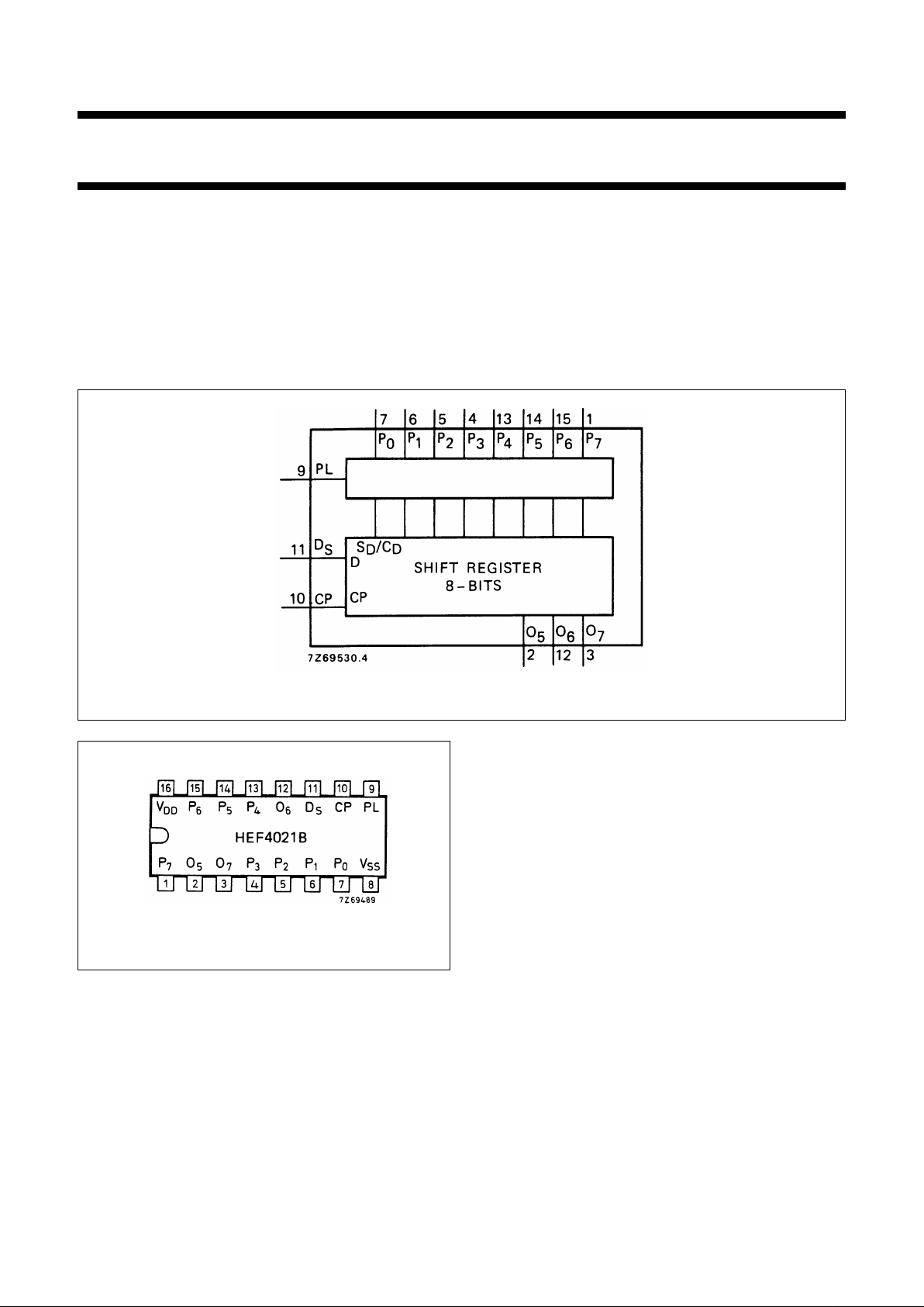
The HEF4021B is an 8-bit static shift register
(parallel-to-serial converter) with a synchronous serial
data input (DS), a clock input (CP), an asynchronous active
HIGH parallel load input (PL), eight asynchronous parallel
data inputs (P0to P7) and buffered parallel outputs from
the last three stages (05to O7).
Each register stage is a D-type master-slave flip-flop with
a set direct/clear direct input. Information on P
0
to P7is
asynchronously loaded into the register while PL is HIGH,
independent of CP and DS. When PL is LOW, data on
DSis shifted into the first register position and all the data
in the register is shifted one position to the right on the
LOW to HIGH transition of CP. Schmitt-trigger action in the
clock input makes the circuit highly tolerant to slower clock
rise and fall times.
Fig.1 Functional diagram.
Fig.2 Pinning diagram.
FAMILY DATA, IDDLIMITS category MSI
See Family Specifications
HEF4021BP(N): 16-lead DIL; plastic
(SOT38-1)
HEF4021BD(F): 16-lead DIL; ceramic (cerdip)
(SOT74)
HEF4021BT(D): 16-lead SO; plastic
(SOT109-1)
( ): Package Designator North America
PINNING
PL parallel load input
P
0
to P
7
parallel data inputs
D
S
serial data input
CP clock input (LOW to HIGH edge-triggered)
O
5
to O
7
buffered parallel outputs from the last three stages
Page 3
January 1995 3
Philips Semiconductors Product specification
8-bit static shift register
HEF4021B
MSI
This text is here in white to force landscape pages to be rotated correctly when browsing through the pdf in the Acrobat reader.This text is here in
_white to force landscape pages to be rotated correctly when browsing through the pdf in the Acrobat reader.This text is here inThis text is here in
white to force landscape pages to be rotated correctly when browsing through the pdf in the Acrobat reader. white to force landscape pages to be ...
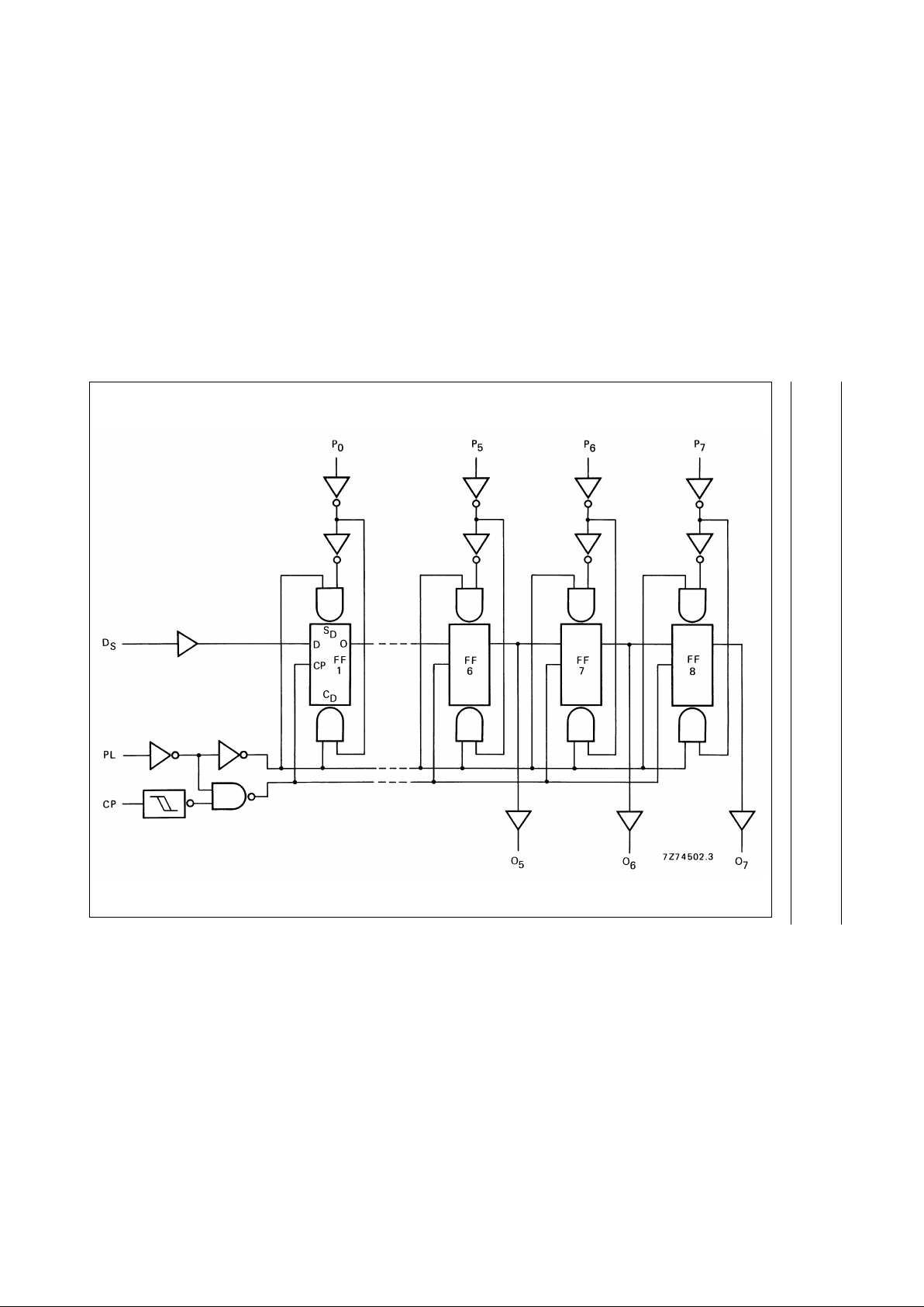
Fig.3 Logic diagram.
Page 4
January 1995 4
Philips Semiconductors Product specification
8-bit static shift register
HEF4021B
MSI
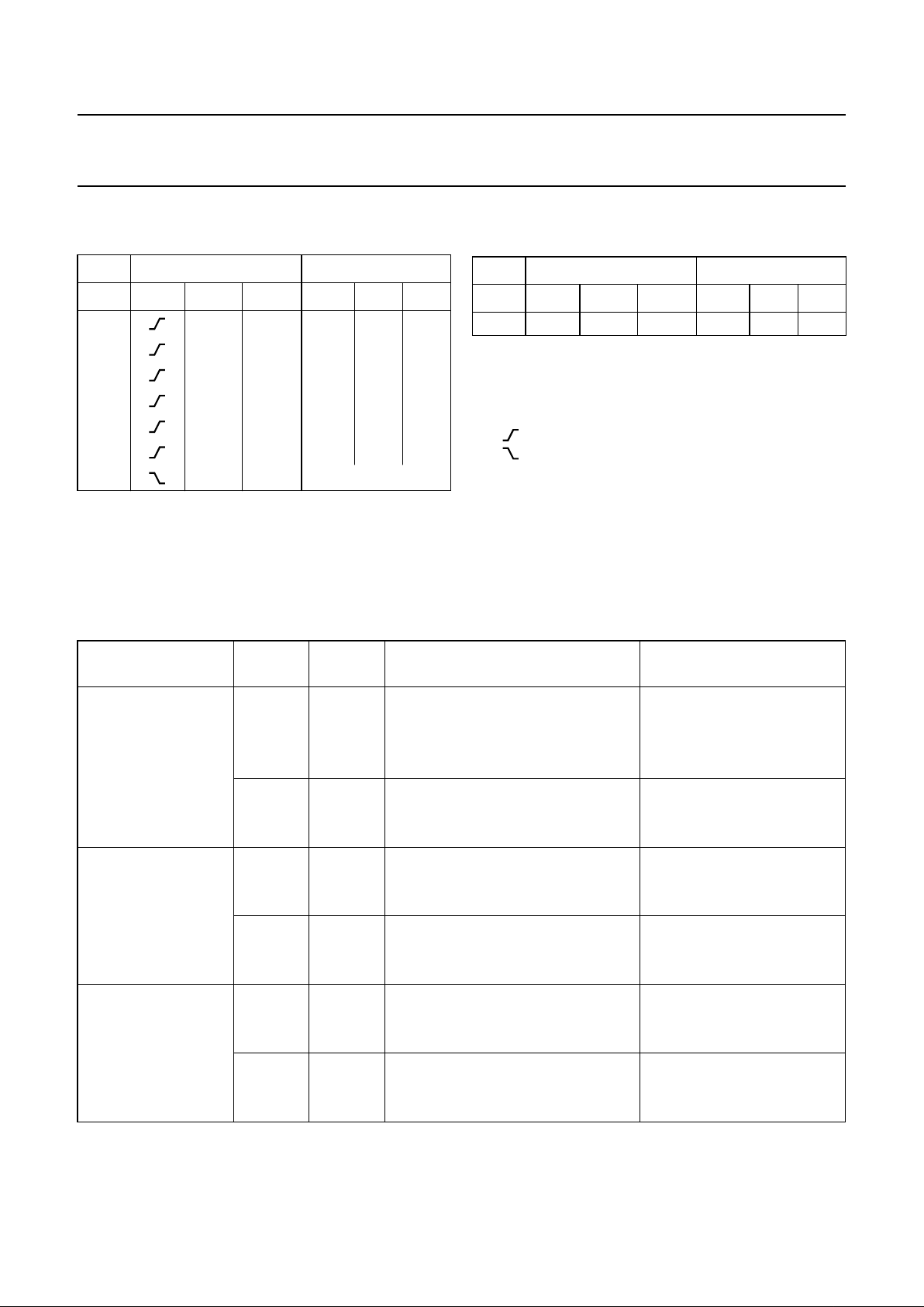
FUNCTION TABLES
Serial operation
INPUTS OUTPUTS
nCPD
S
PL O
5
O
6
O
7
1D
1
LXXX
2D
2
LXXX
3D
3
LXXX
6XLD
1
XX
7XLD
2
D
1
X
8XLD
3
D
2
D
1
X L no change
Parallel operation
Notes
1. H = HIGH state (the more positive voltage)
L = LOW state (the less positive voltage)
X = state is immaterial
= positive-going transition
= negative-going transition
D
n
= either HIGH or LOW
n = number of clock pulse transitions
INPUTS OUTPUTS
nCPD
S
PL O
5
O
6
O
7
XXHP
5
P
6
P
7
AC CHARACTERISTICS
V
SS
= 0 V; T
amb
=25°C; CL= 50 pF; input transition times ≤ 20 ns
V
DD
V
SYMBOL MIN. TYP. MAX.
TYPICAL EXTRAPOLA TION
FORMULA
Propagation delays
CP → O
n
5 125 250 ns 98 ns + (0,55 ns/pF) C
L
HIGH to LOW 10 t
PHL
55 110 ns 44 ns + (0,23 ns/pF) C
L
15 40 80 ns 32 ns + (0,16 ns/pF) C
L
5 115 230 ns 88 ns + (0,55 ns/pF) C
L
LOW to HIGH 10 t
PLH
50 100 ns 39 ns + (0,23 ns/pF) C
L
15 40 80 ns 32 ns + (0,16 ns/pF) C
L
PL → O
n
5 120 240 ns 93 ns + (0,55 ns/pF) C
L
HIGH to LOW 10 t
PHL
55 110 ns 44 ns + (0,23 ns/pF) C
L
15 40 80 ns 32 ns + (0,16 ns/pF) C
L
5 105 210 ns 78 ns + (0,55 ns/pF) C
L
LOW to HIGH 10 t
PLH
50 100 ns 39 ns + (0,23 ns/pF) C
L
15 40 80 ns 32 ns + (0,16 ns/pF) C
L
Output transition 5 60 120 ns 10 ns + (1,0 ns/pF) C
L
times 10 t
THL
30 60 ns 9 ns + (0,42 ns/pF) C
L
HIGH to LOW 15 20 40 ns 6 ns + (0,28 ns/pF) C
L
5 60 120 ns 10 ns + (1,0 ns/pF) C
L
LOW to HIGH 10 t
TLH
30 60 ns 9 ns + (0,42 ns/pF) C
L
15 20 40 ns 6 ns + (0,28 ns/pF) C
L
Page 5
January 1995 5
Philips Semiconductors Product specification
8-bit static shift register
HEF4021B
MSI
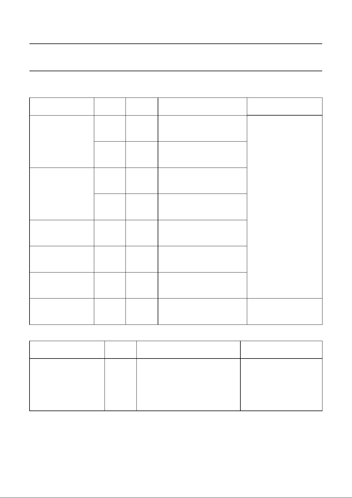
AC CHARACTERISTICS
V
SS
= 0 V; T
amb
=25°C; CL= 50 pF; input transition times ≤ 20 ns
V
DD
V
SYMBOL MIN. TYP. MAX.
Set-up time 5 25 −15 ns
see also waveforms
Figs 4 and 5
DS→ CP 10 t
su
25 −10 ns
15 15 −5ns
55025ns
P
n
→PL 10 t
su
30 10 ns
15 20 5 ns
Hold times 5 40 20 ns
D
S
→ CP 10 t
hold
20 10 ns
15 15 8 ns
515−10 ns
P
n
→ PL 10 t
hold
15 0 ns
15 15 0 ns
Minimum clock 5 70 35 ns
pulse width; LOW 10 t
WCPL
30 15 ns
15 24 12 ns
Minimum PL 5 70 35 ns
pulse width; HIGH 10 t
WPLH
30 15 ns
15 24 12 ns
Recovery time 5 50 10 ns
for PL 10 t
RPL
40 5 ns
15 35 5 ns
Maximum clock 5 6 13 MHz
pulse frequency 10 f
max
15 30 MHz
15 20 40 MHz
V
DD
V
TYPICAL FORMULA FOR P (µW)
Dynamic power 5 900 f
i
+∑(foCL) × V
DD
2
where
dissipation per 10 4 300 f
i
+∑(foCL) × V
DD
2
fi= input freq. (MHz)
package (P) 15 12 000 f
i
+∑(foCL) × V
DD
2
fo= output freq. (MHz)
C
L
= load capacitance (pF)
∑ (f
oCL
) = sum of outputs
V
DD
= supply voltage (V)
Page 6
January 1995 6
Philips Semiconductors Product specification
8-bit static shift register
HEF4021B
MSI
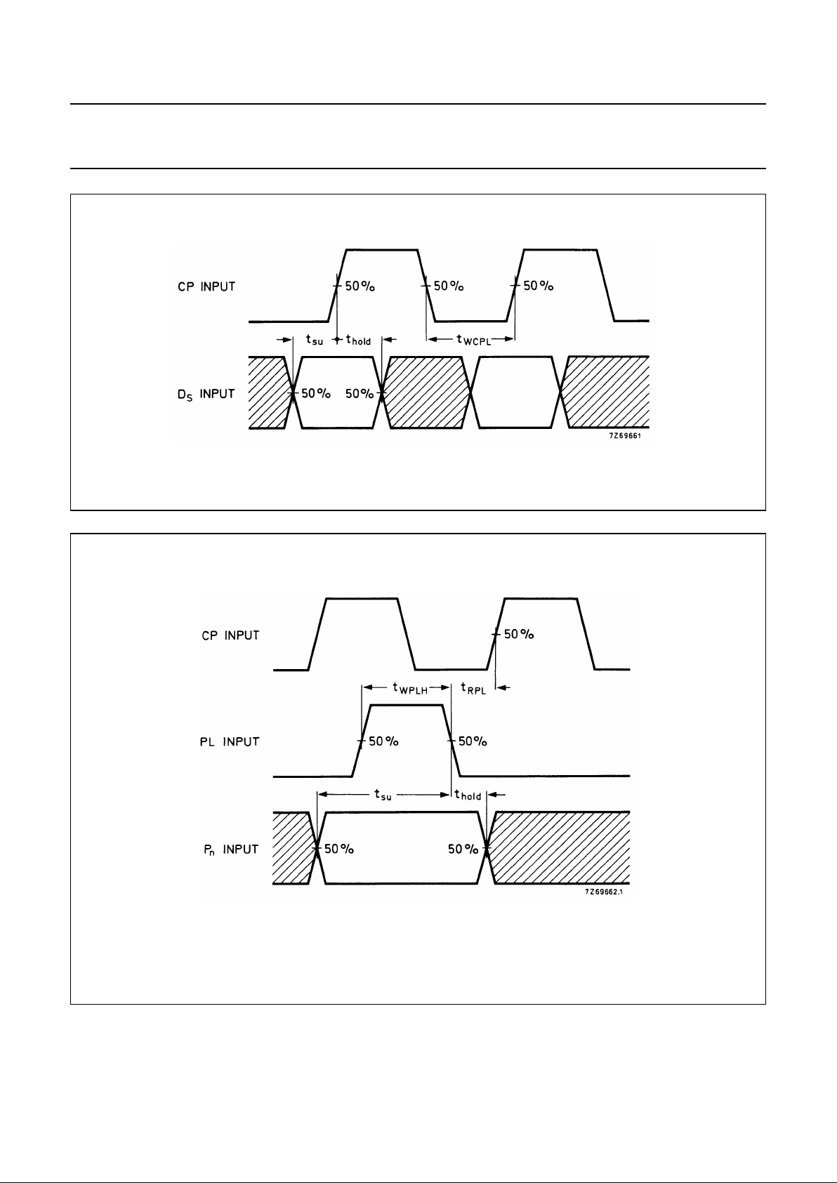
Fig.4 Waveforms showing minimum clock pulse width, set-up time and hold time for CP and DS.
Fig.5 Waveforms showing minimum PL pulse width, recovery time for PL, and set-up and hold times for Pnto
PL. Set-up and hold times are shown as positive values but may be specified as negative values.
 Loading...