Page 1

DATA SH EET
Product specification
File under Integrated Circuits, IC04
January 1995
INTEGRATED CIRCUITS
HEF4017B
MSI
5-stage Johnson counter
For a complete data sheet, please also download:
•The IC04 LOCMOS HE4000B Logic
Family Specifications HEF, HEC
•The IC04 LOCMOS HE4000B Logic
Package Outlines/Information HEF, HEC
Page 2

January 1995 2
Philips Semiconductors Product specification
5-stage Johnson counter
HEF4017B
MSI
DESCRIPTION
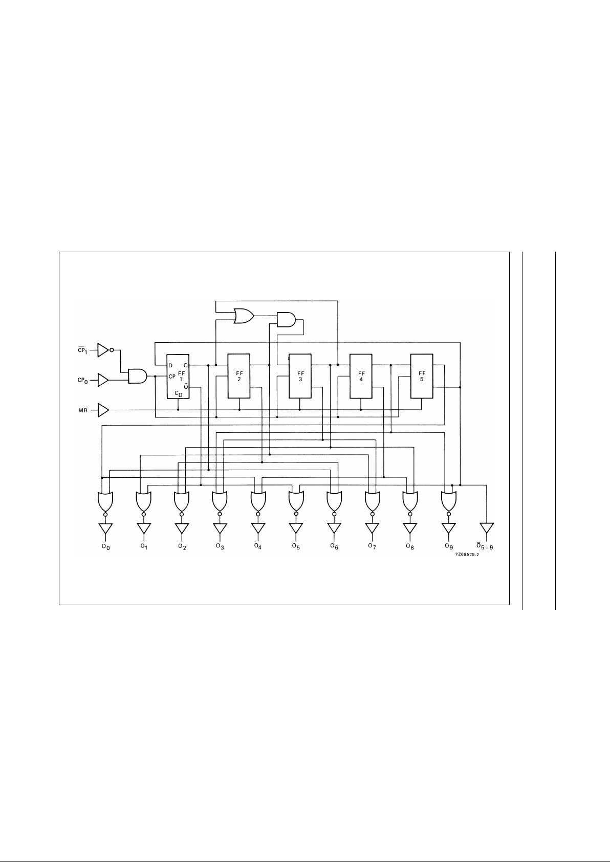
The HEF4017B is a 5-stage Johnson decade counter with
ten spike-free decoded active HIGH outputs (Ooto O9), an
active LOW output from the most significant flip-flop (O
5-9
),
active HIGH and active LOW clock inputs (CP0, CP1) and
an overriding asynchronous master reset input (MR).
The counter is advanced by either a LOW to HIGH
transition at CP0while CP1is LOW or a HIGH to LOW
transition at CP1while CP0is HIGH (see also function
table).
When cascading counters, the
O
5-9
output, which is LOW
while the counter is in states 5, 6, 7, 8 and 9, can be used
to drive the CP0input of the next counter.
A HIGH on MR resets the counter to zero
(O
o
= O
5-9
= HIGH; O1to O9= LOW) independent of the
clock inputs (CP0, CP1).
Automatic code correction of the counter is provided by an
internal circuit: following any illegal code the counter
returns to a proper counting mode within 11 clock pulses.
Schmitt-trigger action in the clock input makes the circuit
highly tolerant to slower clock rise and fall times.
Fig.1 Functional diagram.
HEF4017BP(N): 16-lead DIL; plastic (SOT38-1)
HEF4017BD(F): 16-lead DIL; ceramic (cerdip) (SOT74)
HEF4017BT(D): 16-lead SO; plastic (SOT109-1)
( ): Package Designator North America
Fig.2 Pinning diagram.
PINNING
FAMILY DATA, I
DD
LIMITS category MSI
See Family Specifications
CP
0
clock input (LOW to HIGH triggered)
CP
1
clock input (HIGH to LOW triggered)
MR master reset input
O
0
to O
9
decoded outputs
O
5-9
carry output (active LOW)
Page 3

January 1995 3
Philips Semiconductors Product specification
5-stage Johnson counter
HEF4017B
MSI
This text is here in white to force landscape pages to be rotated correctly when browsing through the pdf in the Acrobat reader.This text is here in
_white to force landscape pages to be rotated correctly when browsing through the pdf in the Acrobat reader.This text is here inThis text is here in
white to force landscape pages to be rotated correctly when browsing through the pdf in the Acrobat reader. white to force landscape pages to be ...
Fig.3 Logic diagram.
Page 4

January 1995 4
Philips Semiconductors Product specification
5-stage Johnson counter
HEF4017B
MSI
FUNCTION TABLE
MR CP
0
CP
1
OPERATION
HXXO
0
=O
5-9
= H; O1to O9=L
L H Counter advances
L L Counter advances
L L X No change
L X H No change
L H No change
L L No change
Notes
1. H = HIGH state (the more positive voltage)
2. L = LOW state (the less positive voltage)
3. X = state is immaterial
4. = positive-going transition
5. = negative-going transition
AC CHARACTERISTICS
V
SS
= 0 V; T
amb
=25°C; CL= 50 pF; input transition times ≤ 20 ns
V
DD
V
SYMBOL MIN. TYP. MAX.
TYPICAL EXTRAPOLA TION
FORMULA
Propagation delays
CP0, CP1→ O0to O
9
5 140 280 ns 113 ns + (0,55 ns/pF) C
L
HIGH to LOW 10 t
PHL
55 110 ns 44 ns + (0,23 ns/pF) C
L
15 40 80 ns 32 ns + (0,16 ns/pF) C
L
5 125 250 ns 98 ns + (0,55 ns/pF) C
L
LOW to HIGH 10 t
PLH
50 100 ns 39 ns + (0,23 ns/pF) C
L
15 40 80 ns 32 ns + (0,16 ns/pF) C
L
CP0, CP1→ O
5-9
5 145 290 ns 118 ns + (0,55 ns/pF) C
L
HIGH to LOW 10 t
PHL
55 110 ns 44 ns + (0,23 ns/pF) C
L
15 40 80 ns 32 ns + (0,16 ns/pF) C
L
5 125 250 ns 98 ns + (0,55 ns/pF) C
L
LOW to HIGH 10 t
PLH
50 100 ns 39 ns + (0,23 ns/pF) C
L
15 40 80 ns 32 ns + (0,16 ns/pF) C
L
MR → O1to O
9
5 115 230 ns 88 ns + (0,55 ns/pF) C
L
HIGH to LOW 10 t
PHL
50 100 ns 39 ns + (0,23 ns/pF) C
L
15 35 70 ns 27 ns + (0,16 ns/pF) C
L
MR → O
5-9
5 110 220 ns 83 ns + (0,55 ns/pF) C
L
LOW to HIGH 10 t
PLH
45 90 ns 34 ns + (0,23 ns/pF) C
L
15 35 70 ns 27 ns + (0,16 ns/pF) C
L
MR → O
0
5 130 260 ns 103 ns + (0,55 ns/pF) C
L
LOW to HIGH 10 t
PLH
55 105 ns 44 ns + (0,23 ns/pF) C
L
15 40 75 ns 32 ns + (0,16 ns/pF) C
L
Page 5

January 1995 5
Philips Semiconductors Product specification
5-stage Johnson counter
HEF4017B
MSI
AC CHARACTERISTICS
V
SS
= 0 V; T
amb
=25°C; CL= 50 pF; input transition times ≤ 20 ns
Output transition
times 5 60 120 ns 10 ns + (1,0 ns/pF) C
L
HIGH to LOW 10 t
THL
30 60 ns 9 ns + (0,42 ns/pF) C
L
15 20 40 ns 6 ns + (0,28 ns/pF) C
L
5 60 120 ns 10 ns + (1,0 ns/pF) C
L
LOW to HIGH 10 t
TLH
30 60 ns 9 ns + (0,42 ns/pF) C
L
15 20 40 ns 6 ns + (0,28 ns/pF) C
L
V
DD
V
SYMBOL MIN. TYP. MAX.
Hold times 5 90 45 ns
CP
0
→CP
1
10 t
hold
40 20 ns
15 20 10 ns
58040ns
CP1→ CP
0
10 t
hold
40 20 ns
15 30 10 ns
Minimum clock
pulse width: 5
t
WCPL
=
t
WCPH
80 40 ns
CP
0
= LOW; 10 40 20 ns see also waveforms
CP1= HIGH 15 30 15 ns Figs 4 and 5
Minimum MR 5 50 25 ns
pulse width; HIGH 10 t
WMRH
30 15 ns
15 20 10 ns
Recovery time 5 60 30 ns
for MR 10 t
RMR
30 15 ns
15 20 10 ns
Maximum clock 5 6 12 MHz
pulse frequency 10 f
max
12 24 MHz
15 15 30 MHz
V
DD
V
TYPICAL FORMULA FOR P (µW)
Dynamic power 5 500 f
i
+∑(foCL) × V
DD
2
where
dissipation per 10 2200 f
i
+∑(foCL) × V
DD
2
fi= input freq. (MHz)
package (P) 15 6000 f
i
+∑(foCL) × V
DD
2
fo= output freq. (MHz)
C
L
= load cap. (pF)
∑ (f
oCL
) = sum of outputs
V
DD
= supply voltage (V)
V
DD
V
SYMBOL MIN. TYP. MAX.
TYPICAL EXTRAPOLA TION
FORMULA
Page 6

January 1995 6
Philips Semiconductors Product specification
5-stage Johnson counter
HEF4017B
MSI
Fig.4 Waveforms showing hold times for CP0to CP1and CP1to CP0. Hold times are shown as positive values,
but may be specified as negative values.
Fig.5 Waveforms showing recovery time for MR; minimum CP0and MR pulse widths.
Conditions: CP1= LOW while CP0is triggered on a LOW to HIGH transition. t
WCP
and
t
RMR
also apply when CP0= HIGH and CP1is triggered on a HIGH to LOW transition.
Page 7

January 1995 7
Philips Semiconductors Product specification
5-stage Johnson counter
HEF4017B
MSI
Fig.6 Timing diagram.
Page 8

January 1995 8
Philips Semiconductors Product specification
5-stage Johnson counter
HEF4017B
MSI
APPLICATION INFORMATION
Some examples of applications for the HEF4017B are:
• Decade counter with decimal decoding
• 1 out of n decoding counter (when cascaded)
• Sequential controller
• Timer.
Figure 7 shows a technique for extending the number of decoded output states for the HEF4017B. Decoded outputs are
sequential within each stage and from stage to stage, with no dead time (except propagation delay).
Note
It is essential not to enable the counter on
CP1when CP0is HIGH, or on CP0when CP1is LOW, as the this would cause
an extra count.
Fig.7 Counter expansion.
 Loading...