

Datasheet HEF4007UBU, HEF4007UBT, HEF4007UBPB, HEF4007UBP, HEF4007UBDB Datasheet (Philips)
...Page 1

DATA SH EET
Product specification
File under Integrated Circuits, IC04
January 1995
INTEGRATED CIRCUITS
HEF4007UB
gates
Dual complementary pair and
inverter
For a complete data sheet, please also download:
•The IC04 LOCMOS HE4000B Logic
Family Specifications HEF, HEC
•The IC04 LOCMOS HE4000B Logic
Package Outlines/Information HEF, HEC
Page 2
January 1995 2
Philips Semiconductors Product specification
Dual complementary pair and inverter
HEF4007UB
gates
DESCRIPTION
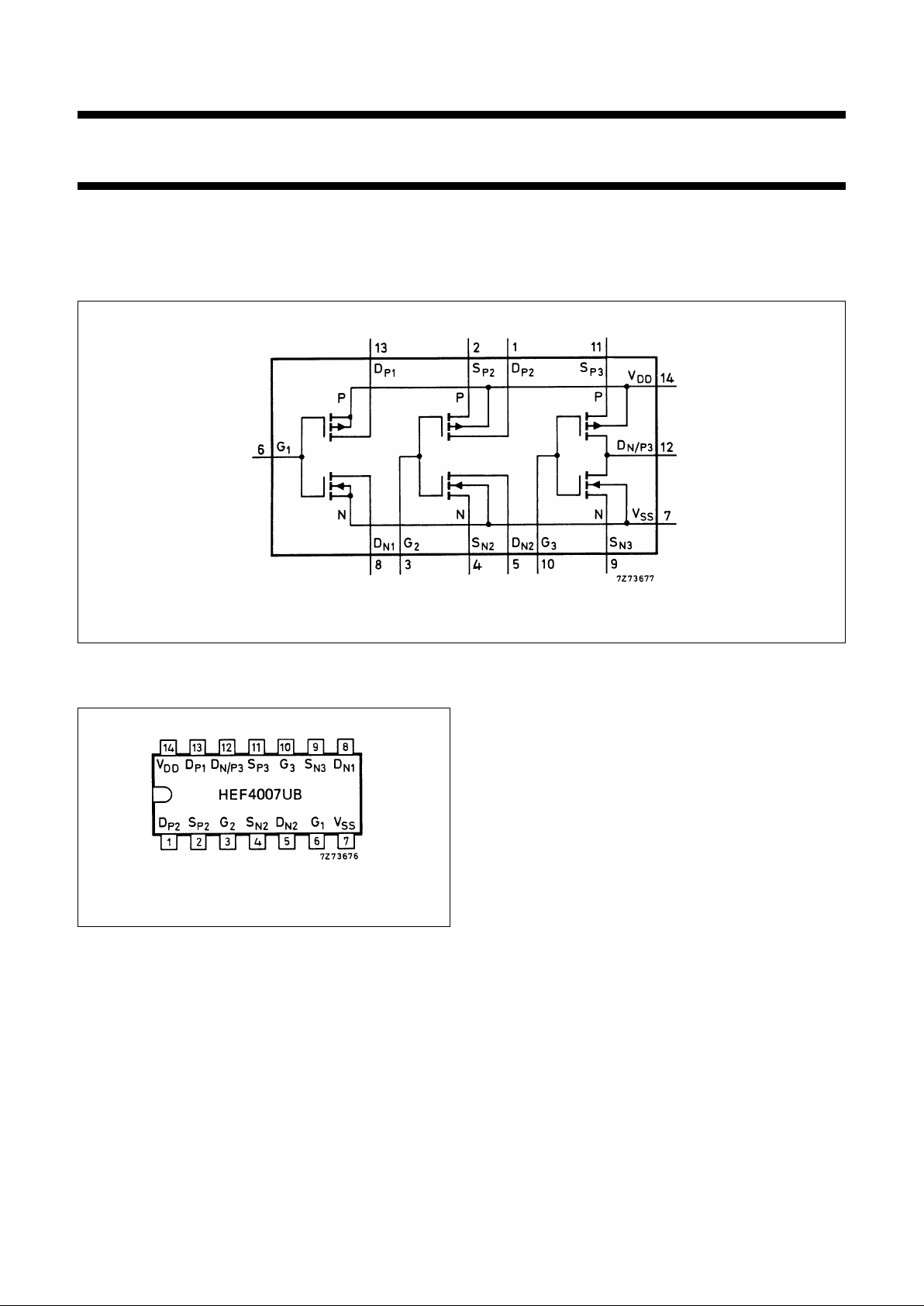
The HEF4007UB is a dual complementary pair and an inverter with access to each device. It has three n-channel and
three p-channel enhancement mode MOS transistors.
Fig.1 Schematic diagram.
HEF4007UBP(N): 14-lead DIL; plastic
(SOT27-1)
HEF4007UBD(F): 14-lead DIL; ceramic (cerdip)
(SOT73)
HEF4007UBT(D): 14-lead SO; plastic
(SOT108-1)
( ): Package Designator North America
Fig.2 Pinning diagram.
PINNING
FAMILY DATA, I
DD
LIMITS category GATES
See Family Specifications for V
IH/VIL
unbuffered stages
S
P2
, S
P3
source connections to 2nd and 3rd
p-channel transistors
D
P1
, D
P2
drain connections from the 1st and 2nd
p-channel transistors
D
N1,DN2
drain connections from the 1st and 2nd
n-channel transistors
S
N2,SN3
source connections to the 2nd and 3rd
n-channel transistors
D
N/P3
common connection to the 3rd p-channel
and n-channel transistor drains
G
1
to G3gate connections to n-channel and
p-channel of the three transistor pairs
Page 3

January 1995 3
Philips Semiconductors Product specification
Dual complementary pair and inverter
HEF4007UB
gates
AC CHARACTERISTICS
V
SS
= 0 V; T
amb
=25°C; CL= 50 pF; input transition times ≤ 20 ns
V
DD
V
SYMBOL TYP. MAX.
TYPICAL EXTRAPOLATION
FORMULA
Propagation delays
Gn→ DN; D
P
5 40 80 ns 13 ns + (0,55 ns/pF) C
L
HIGH to LOW 10 t
PHL
20 40 ns 9 ns + (0,23 ns/pF) C
L
15 15 30 ns 7 ns + (0,16 ns/pF) C
L
5 40 75 ns 13 ns + (0,55 ns/pF) C
L
LOW to HIGH 10 t
PLH
20 40 ns 9 ns + (0,23 ns/pF) C
L
15 15 30 ns 7 ns + (0,16 ns/pF) C
L
Output transition times 5 60 120 ns 10 ns + (1,0 ns/pF) C
L
HIGH to LOW 10 t
THL
30 60 ns 9 ns + (0,42 ns/pF) C
L
15 20 40 ns 6 ns + (0,28 ns/pF) C
L
5 60 120 ns 10 ns + (1,0 ns/pF) C
L
LOW to HIGH 10 t
TLH
30 60 ns 9 ns + (0,42 ns/pF) C
L
15 20 40 ns 6 ns + (0,28 ns/pF) C
L
V
DD
V
TYPICAL FORMULA FOR P (µW)
Dynamic power 5 4500 f
i
+∑(foCL) × V
DD
2
where
dissipation per 10 20 000 f
i
+∑(foCL) × V
DD
2
fi= input freq. (MHz)
package (P) 15 50 000 f
i
+∑(foCL) × V
DD
2
fo= output freq. (MHz)
C
L
= load capacitance (pF)
∑(f
oCL
) = sum of outputs
V
DD
= supply voltage (V)
Page 4
January 1995 4
Philips Semiconductors Product specification
Dual complementary pair and inverter
HEF4007UB
gates
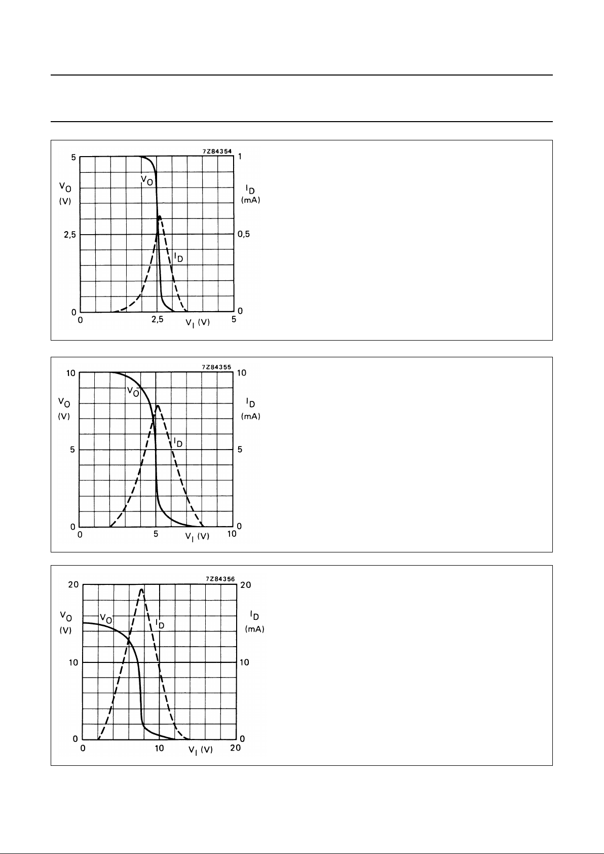
Fig.3 Typical drain current IDand output voltage VOas
functions of input voltage; VDD= 5 V; T
amb
= 25 °C.
Fig.4 Typical drain current IDand output voltage VOas
functions of input voltage; VDD= 10 V; T
amb
= 25 °C.
Fig.5 Typical drain current IDand output voltage VOas
functions of input voltage; VDD= 15 V; T
amb
= 25 °C.
Page 5
January 1995 5
Philips Semiconductors Product specification
Dual complementary pair and inverter
HEF4007UB
gates
APPLICATION INFORMATION
Some examples of applications for the HEF4007UB are:
• High input impedance amplifiers
• Linear amplifiers
• (Crystal) oscillators
• High-current sink and source drivers
• High impedance buffers.
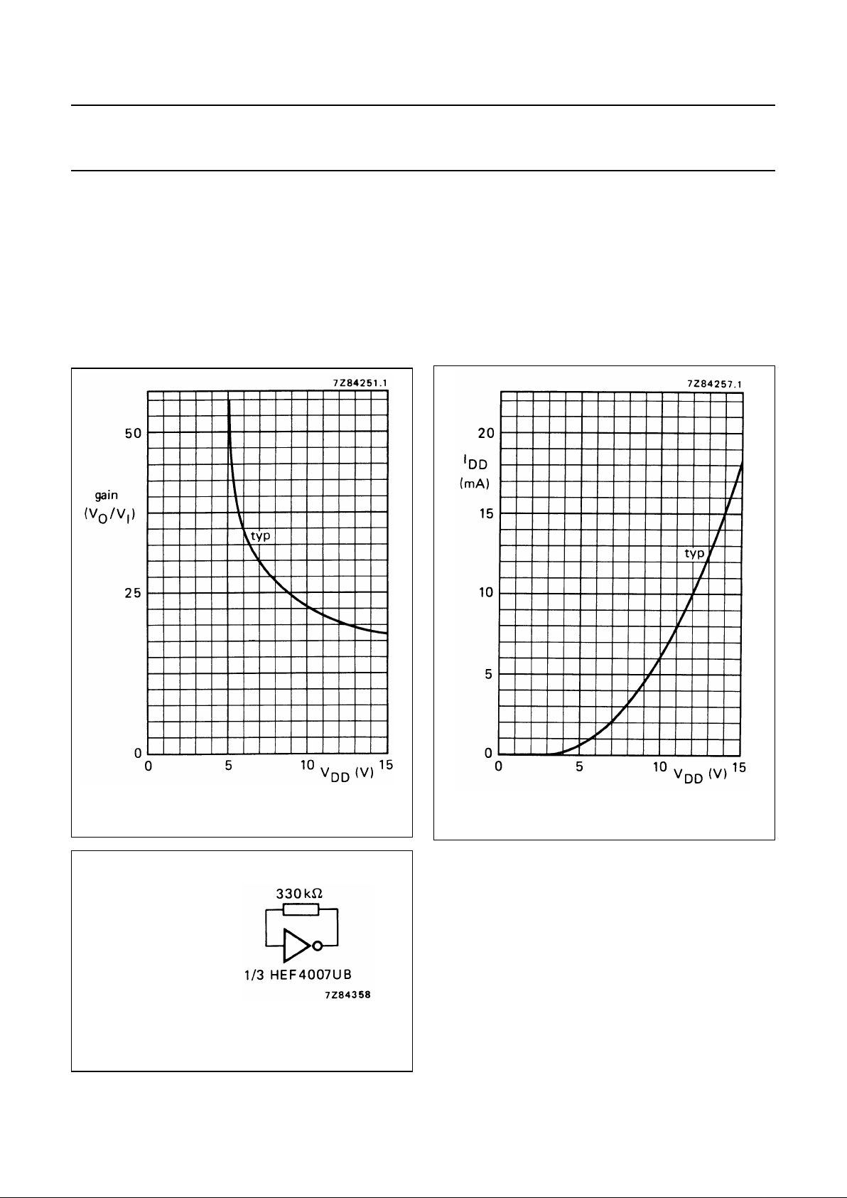
Fig.6 Voltage gain (Vo/Vi) as a function of supply
voltage.
Fig.7 Supply current as a function of supply
voltage.
Fig.8 Test set-up for measuring graphs of Figs 6
and 7.
This is also an example of an
analogue amplifier using one
HEF4007UB gate.
Page 6
January 1995 6
Philips Semiconductors Product specification
Dual complementary pair and inverter
HEF4007UB
gates
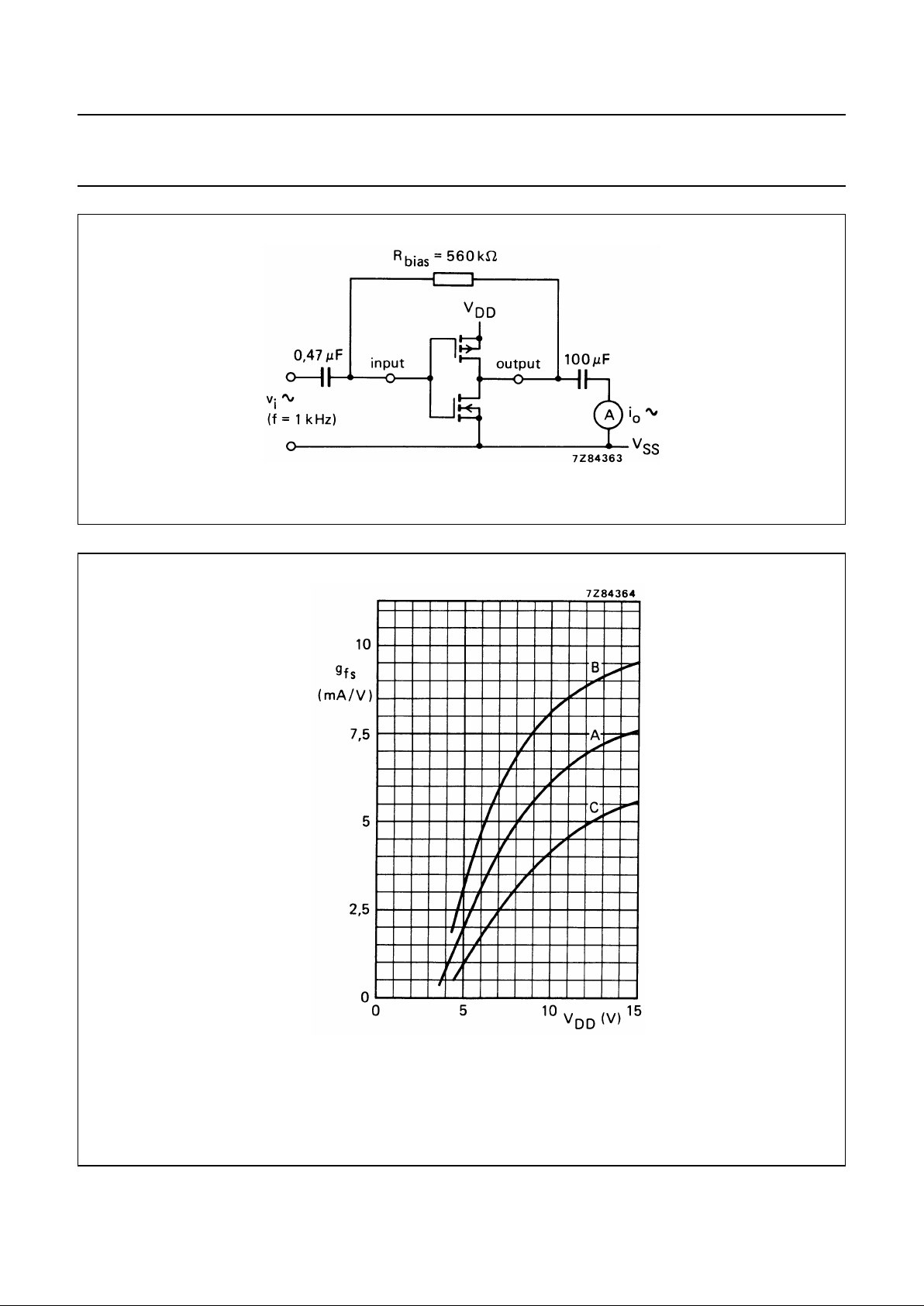
Fig.9 Test set-up for measuring forward transconductance gfs=dio/dviat vois constant (see also graph Fig.10).
Fig.10 Typical forward transconductance gfsas a function of the supply voltage at T
amb
=25°C.
A: average,
B: average + 2 s,
C: average − 2 s, in where ‘s’ is the observed standard deviation.
Page 7
January 1995 7
Philips Semiconductors Product specification
Dual complementary pair and inverter
HEF4007UB
gates
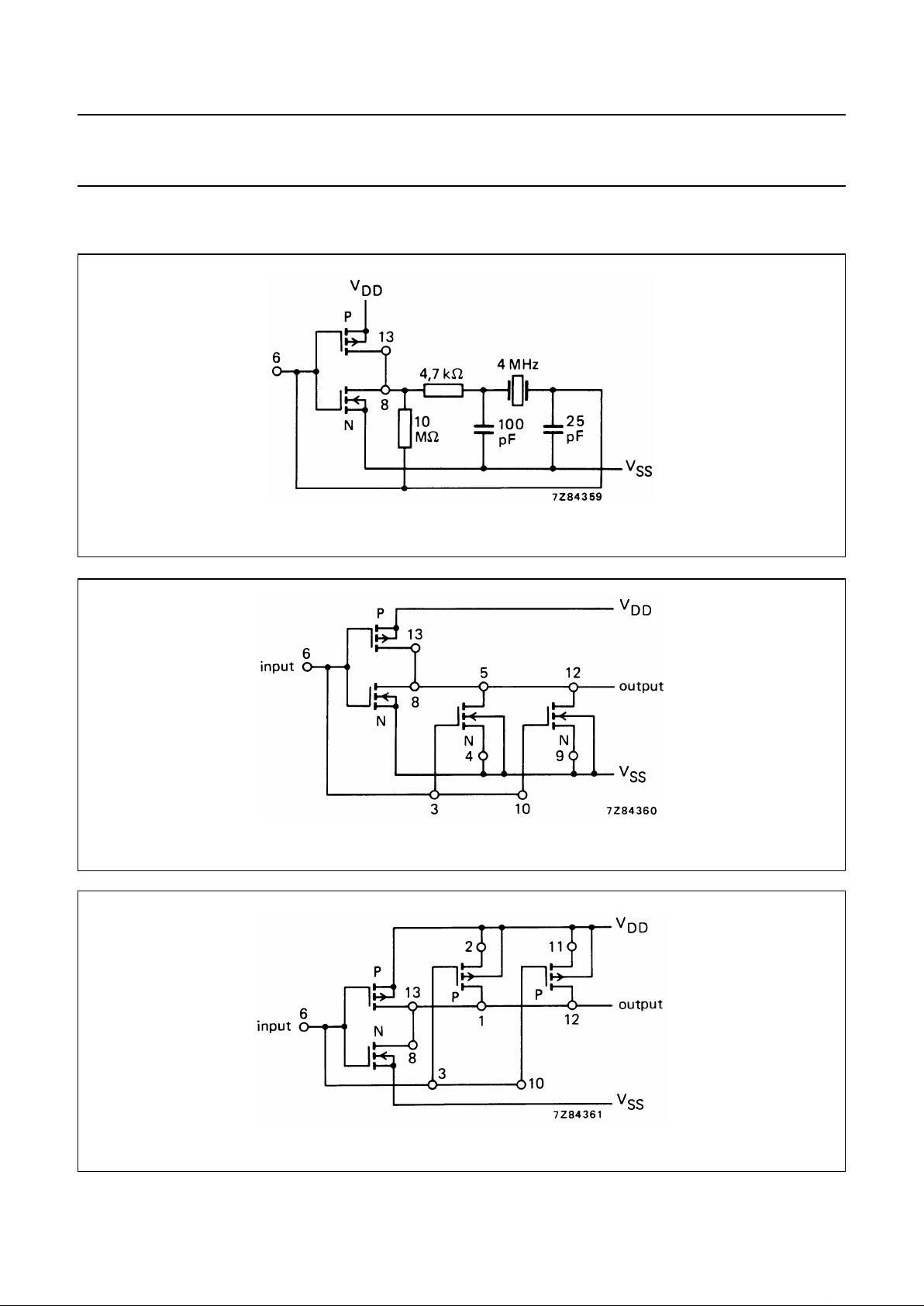
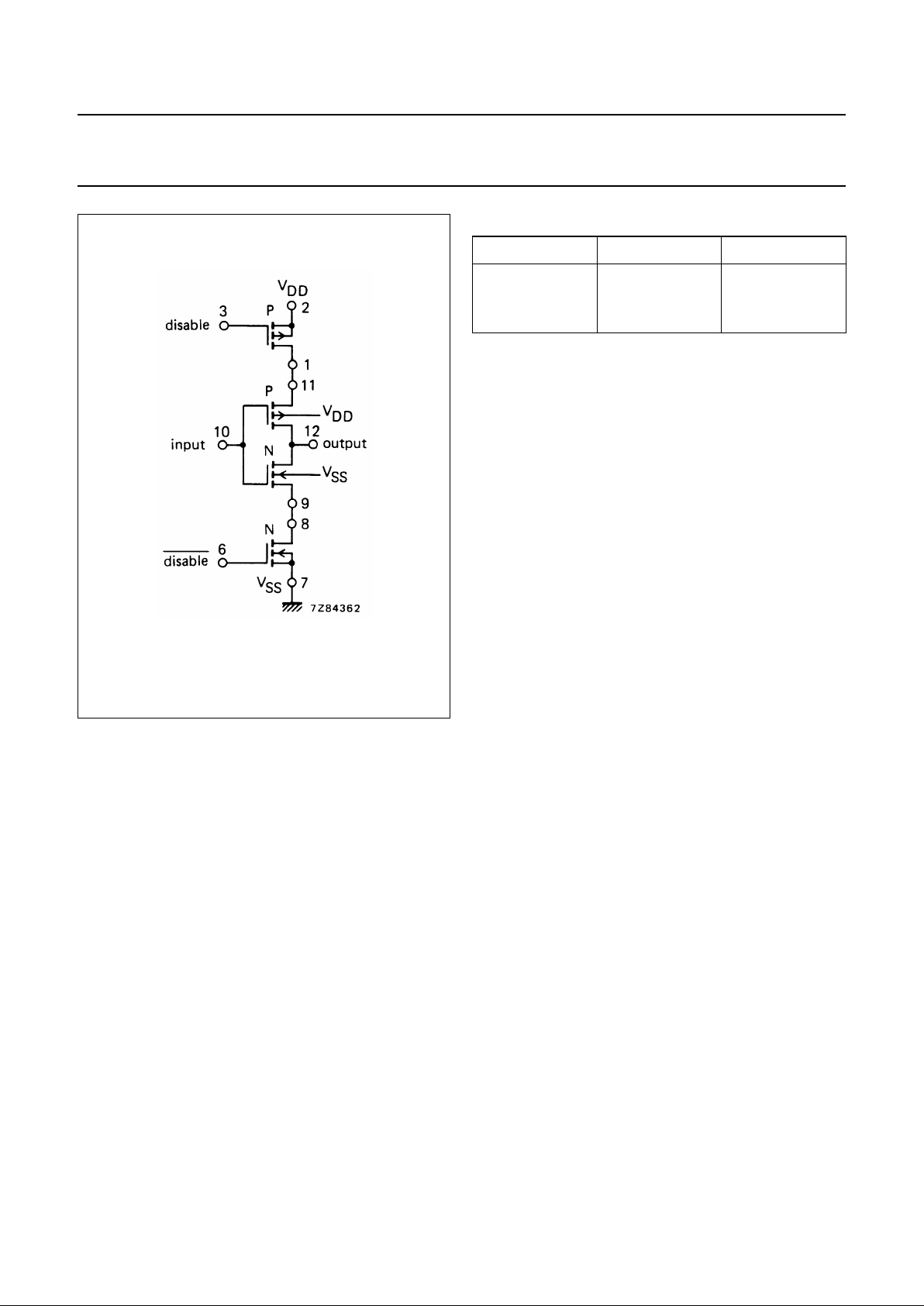
Figures 11 to 14 show some applications in which the HEF4007UB is used.
Fig.11 4 MHz crystal oscillator.
Fig.12 High current sink driver.
Fig.13 High current source driver.
Page 8
January 1995 8
Philips Semiconductors Product specification
Dual complementary pair and inverter
HEF4007UB
gates
Fig.14 High impedance buffer.
FUNCTION TABLE for Fig.14.
Notes
1. H = HIGH state (the more positive voltage)
L = LOW state (the less positive voltage)
X = state is immaterial
NOTE
Rules for maintaining electrical isolation between
transistors and monolithic substrate:
• Pin number 14 must be maintained at the most positive
(or equally positive) potential with respect to any other
pin of the HEF4007UB.
• Pin number 7 must be maintained at the most negative
(or equally negative) potential with respect to any other
pin of the HEF4007UB.
Violation of these rules will result in improper transistor
operation and/or possible permanent damage to the
HEF4007UB.
INPUT DISABLE OUTPUT
HLL
LLH
X H open
 Loading...