

Page 1

1
HDM8513A Users Manual
DVB/DSS Compliant Receiver
Nov. 2000
Revision 1.0
Page 2

2
Page 3

3
Direct Broadcast Satellite (DBS) has been one of the most succe ssful new product
introductions in the history of consumer electronics. This product represents the first
application of digital video compression for broadcast television. Originally intended to
provide cable quality television services to remote areas, this product is now offering a
competitive replacement to cable services in many urban areas.
The first operational systems employ closed proprietary signaling structures. The
European Broadcasting Union (EBU) has developed the first open standard (DVB-S) for
DBS services. The broadcasting community has embraced this standard which is now
being adopted for new systems throughout the world. This widely accepted open
standard is essential for DBS to achieve full market potential.
The HDM8513ATM is a fully DVB-S&DSS compliant ADC/QPSK demodulator/FEC
device which provides an MPEG-2 stream to be processed by the conditional access
and video decompression circuits. The demodulator clocked with a fixed frequency is
true variable rate over the range of 1 t o 55M symbols-per-second. This product
achieves the highest performance and flexibility. It minimizes the cost of external
circuits, thus reducing overall system cost.
Page 4

4
Hynix Semiconductor Co., Lt d reserves the right to make changes to its products or
specifications to improve performance, reliability, or manufacturability. Information
furnished by Hynix Semiconducto r Co., Ltd is believed to be accurate and reliable.
However, no responsibility is ass umed by Hynix Semiconductor Co., Ltd for its use; nor
for any infringement of patents or other rights of third parties which may result from its
use. No license is granted by its implication or otherwise unde r any patent rights of
Hy nix Semiconductor Co., Ltd.
For more information contact:
Address: Youngdong Bldg. 891, Daechi-dong, Kangnam-gu, Seoul, 135-738, Korea
Tel: 82-2 -3459-3188
Fax: 82-2 -3459-5843
E-mail: [email protected]
Page 5

5
TABLE OF CONTENTS
1. INTRODUCTION TO THE HDM8513A ................................................................................................................7
1.1 FEATURES AND BENEFITS..................................................................................................................................8
2. HARDWARE SPECIFICATION..............................................................................................................................9
3. TECHNICAL OVERVIE W.....................................................................................................................................19
3.1 DUAL CHANNEL ANALOG TO DIGITAL CONVERTER .................................................................................. 19
3.2 V ARIABLE RATE DEMODULATOR.................................................................................................................. 21
3.3 NOISE MEASUREMENT CIRCUIT.....................................................................................................................23
3.4 V ITERBI DECODER.............................................................................................................................................25
3.5 AUTONOMOUS ACQUISITION..........................................................................................................................26
3.6 REED SOLOMON DECODER..............................................................................................................................28
3.7 CLOCK G ENERATION PLL .................................................................................................................................30
3.8 DBS R ECEIVER...................................................................................................................................................31
4. MECHANICAL SPECIFICATION S..................................................................................................................... 32
4.1 100 P IN Q UAD FLAT PACK................................................................................................................................32
4.2 64 P IN THIN QUAD FLAT PACK........................................................................................................................34
4.3 RECOMMENDED ANALOG P IN CONNECTION...............................................................................................36
4.4 RECOMMENDED CLOCK G ENERATION CIRCUIT...........................................................................................36
5. SIGNAL DESCRIPTION....................................................................................................................................... 37
5.1 INPUTS..................................................................................................................................................................37
5.2 OUTPUTS.............................................................................................................................................................37
5.3 MONITOR AND CONTROL INTERFACE ...........................................................................................................40
5.4 I2C MODE.............................................................................................................................................................41
6. REGISTER DEFINITIONS.....................................................................................................................................43
6.1 WRITE REGISTERS..............................................................................................................................................43
6.2 READ REGISTERS................................................................................................................................................56
APPENDIX....................................................................................................................................................................59
A1. L OOP FILTER PROGRAMMING APPLICATION NOTE................................................................................60
A2. FALSE LOCK ESCAPE APPLICATION NOTE.................................................................................................63
A3. PERFORMANCE WITH INTERFERENCE. .........................................................................................................64
A4. NYQUIST CRITERIA CONSIDERATIONS.........................................................................................................68
LIST OF FIGURES
FIGURE 1: T OP LEVEL BLOCK DIAGRAM....................................................................................................................7
FIGURE 2: I NPUT DATA TIMING DIAGRAM.............................................................................................................10
FIGURE 3: I NTEL 80C88A READ TIMING DIAGRAM...............................................................................................11
FIGURE 4: I NTEL 80C88A WRITE TIMING DIAGRAM.............................................................................................12
FIGURE 5: I NTEL 8051 READ TIMING DIAGRAM.....................................................................................................13
FIGURE 6: I NTEL 8051 WRITE TIMING DIAGRAM...................................................................................................14
Page 6

6
FIGURE 7: MOTOROLA READ TIMING D IAGRAM....................................................................................................15
FIGURE 8: MOTOROLA WRITE TIMING DIAGRAM.................................................................................................16
FIGURE 9: O UTPUT TIMING DIAGRAM FOR NORMAL PARALLEL....................................................................... 17
FIGURE 10 : OUTPUT TIMING DIAGRAM FOR NORMAL SERIAL...........................................................................17
FIGURE 11: OUTPUT TIMING DIAGRAM FOR REGULATED PARALLEL...............................................................18
FIGURE 12: OUTPUT TIMING DIAGRAM FOR REGULATED SERIAL MODE1.......................................................18
FIGURE 13: OUTPUT TIMING DIAGRAM FOR REGULATED SERIAL MODE2.......................................................18
FIGURE 14: ADC B LOCK DIAGRAM............................................................................................................................ 20
FIGURE 15: DEMODULATOR BLOCK DIAGRAM .......................................................................................................21
FIGURE 16: NOISE MEASUREMENT CIRCUIT...........................................................................................................23
FIGURE 17: NOISE ACCUMULATOR AS A FUNCTION OF SNR AND TIME............................................................ 24
FIGURE 18: V ITERBI D ECODER...................................................................................................................................25
FIGURE 19: REED SOLOMON DECODER....................................................................................................................29
FIGURE 20: CLOCK SIGNAL G ENERATION................................................................................................................30
FIGURE 21: TYPICAL SET TOP BOX DEMODULATOR............................................................................................ 31
FIGURE 22: MECHANICAL CONFIGURATION...........................................................................................................33
FIGURE 23: MECHANICAL CONFIGURATION...........................................................................................................35
FIGURE 24: ANALOG PIN CONNECTION.................................................................................................................... 36
FIGURE 25: CLOCK GENERATION CIRCUIT ..........................................................................................................36
FIGURE 26: I2C WRITE TO THE HDM8513A ...........................................................................................................41
FIGURE 27 : I2C READ FROM THE HDM8513A .........................................................................................................42
FIGURE A1: SYMBOL TIMING RECOVERY TRANSIENT RESPONSE....................................................................... 60
FIGURE A2: CARRIER PHASE RECOVERY TRANSIENT RESPONSE........................................................................61
FIGURE A3: CARRIER PHASE RECOVERY TRANSIENT RESPONSE WITH LOW SNR..........................................62
FIGURE A4: ADJACENT CHANNEL INTERFERENCE OF 10 DB, 1.35 SPACING....................................................65
FIGURE A5: PERFORMANCE WITH INTERFERER AT DIFFERENT CARRIER SPACINGS.....................................66
FIGURE A6: PERFORMANCE WITH +10 DB INTERFERER......................................................................................67
LIST OF TABLES
TABLE 1: ABSOLUTE MAXIMUM RATINGS...............................................................................................................9
TABLE 2: DC C HARACTERISTICS.................................................................................................................................9
TABLE 3: D EMODULATOR SPECIFICATIONS...........................................................................................................10
TABLE 4: AC C HARACTERISTICS...............................................................................................................................10
TABLE 5: I NTEL 80C88A READ CYCLE TIMING PARAMETERS (B USMODE = 1)................................................11
TABLE 6: I NTEL 80C88A WRITE CYCLE TIMING PARAMETERS (BUSMODE = 1).............................................12
TABLE 7: I NTEL 8051 READ CYCLE TIMING PARAMETERS (BUSMODE = 1)......................................................13
TABLE 8: I NTEL 8051 WRITE CYCLE TIMING PARAMETERS (BUSMODE = 1)...................................................14
TABLE 9: MOTOROLA READ CYCLE TIMING PARAMETERS (BUSMODE =0).................................................... 15
TABLE 10: MOTOROLA WRITE CYCLE TIMING PARAMETERS (BUSMODE =0).................................................16
TABLE 11: OUTPUT TIMING....................................................................................................................................... 17
TABLE 12: E XAMPLE OF ACQUISITION TIMING.....................................................................................................27
TABLE 13: I2C S LAVE ADDRESS..................................................................................................................................42
Page 7
7
6
6
I
Q
DemodulatorViterb
i
and
Solomon
8Data ClockDataQPSKNode
Fixed Rat
e
Sample Clock33Symbol ClockViterbi Bit ClockFrameSync8Viterb
i
1. Introduction to the HDM8513A
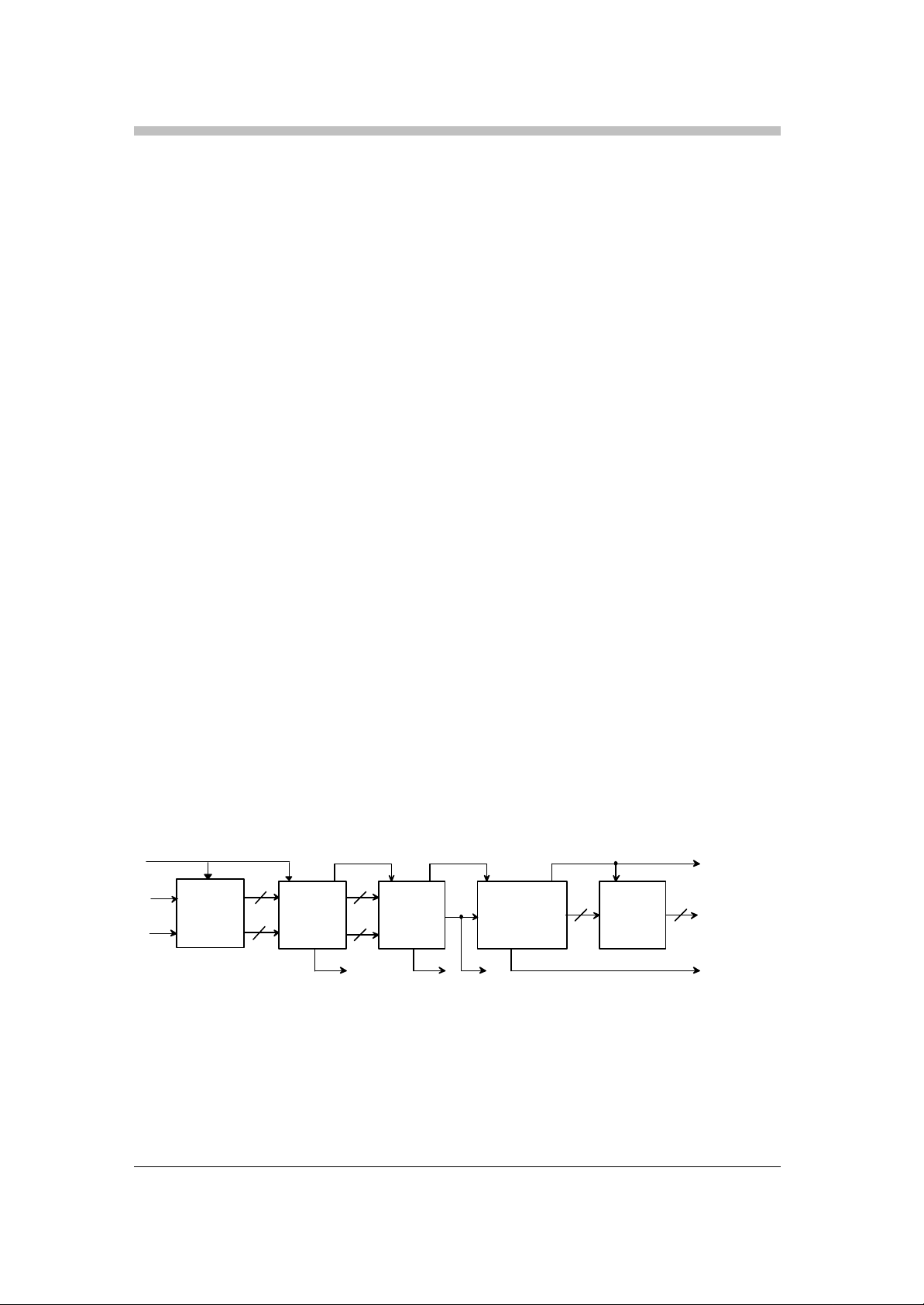
The HDM8513A digital demodulator for direct broadcast satellite receivers is a single chip solution fully
compliant with the European Telecommunications Standards Institute (ETSI) specification ETS 300
421. This chip integrates an A/D converter, a variable rate matched filter, a variable rate QPSK
demodulator with a Viterbi decoder, a deinterleaver and a Reed Solomon decoder.
The HDM8513A, which is implemented in a 0.35 micron CMOS, Triple Layer Metal Process, provides
variable rate capability while operating with a fixed frequency sampling clock. Digital samples of
baseband I and Q data are generated by an internal A/D converter, then provided to the demodulator at
a fixed sample rate. The root raised cosine filter is implemented internally with fully digital techniques.
Similarly, the symbol timing recovery and carrier phase tracking functions are performed entirely in the
digital domain. This approach provides minimum constraints on external circuits, thus reducing overall
system costs.
The HDM8513A may be configured by an external processor for a specific symbol rate, and carrier
frequency along with loop gain parameters. The HDM8513A provides an external AGC signal which is
used to control the gain of the analog signal which is applied to the down-converters. And it also
provides a digital AGC internally which controls the gain of the signal out of the matched filters. In
addition, the HDM8513A provides fully programmable sweep circuitry to aid in initial acquisition when
large frequency offsets may be present.
The digital frequency translation capability of the HDM8513A permits this part to be used in frequency
multiplexing applications. In this application, an entire transponder bandwidth containing many signals
is sampled at a fixed rate. The digital oscillator within the HDM8513A is programmed to the specific
desired carrier frequency within that band to permit the selected signal to be passed through the
baseband filter and processed by the demodulator circuits.
A/D
Converter
Variable
Rate
QPSK
Decoder
Synchronization
Deinterleaving
Reed
Decoder
FIGURE 1: T OP LEVEL BLOCK DIAGRAM
Page 8

8
1.1 Features and Benefits
* Fully DVB&DSS compliant
* Dual 6bit A/D converters
* Continuously variable symbol rate from 1Msps to 55Msps (75MHz clock)
* Internal digital root raised cosine filter
* Less than 0.5 dB implementation loss
* Frequency multiplexing capability
* Automated frequency search
* Internal bias cancellation
* Both wideband and narrowband AGC
* Noise calibration for antenna steering
* Output data rate as high as 68Mbps
* Fixed frequency sampling clock
* Simple interface with tuner and analog processing
* Microcontroller interface
* Eight bit parallel or I2C monitor and control interface
* I2C by -pass mode
* Two package types
Part code Package
HDM8513AP 100PQFP
HDM8513AT 64TQFP
Page 9
9
2. Hardware Specification
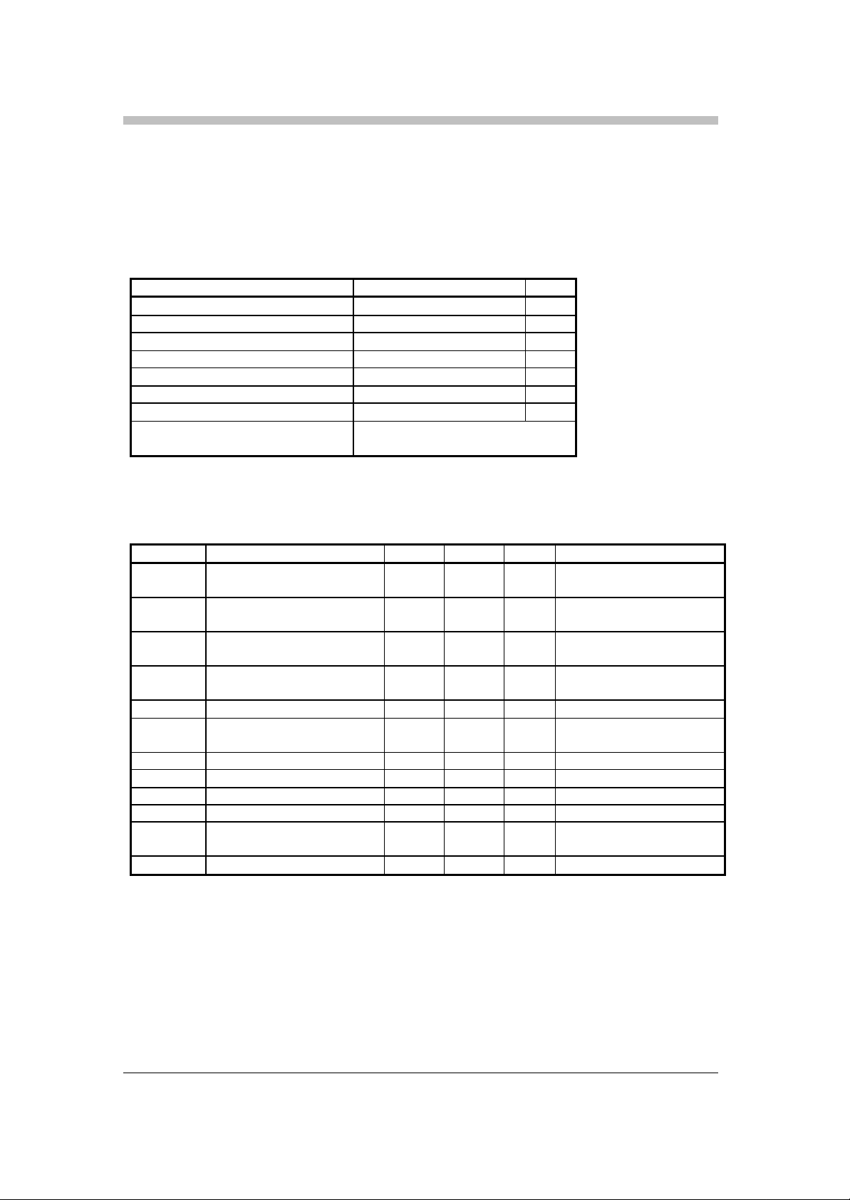
Table 1: Absolute Maximum Ratings
Rating Value Unit
Ambient Temperature under Bias -10 to 70 c
Storage Temperature -65 to 150 c
Ambient Humidity under Bias 85( 85 c,500hrs) %
Thermal Resistance(Ja) 45 c/W
Junction Temperature 150 c
Voltage on Any Pin Vss - 0.3V to VDD + 0.5V V
VDD, IOVDD 5.5 V
Package Material - Compound : CEL -4630SX
Table 2: DC Characteristics
Symbol Parameter Min. Max. Units Test Conditions
IDD Dynamic Current
(Power Supply Current)
IOVDD Interface Power Supply
Voltage
VDD Core Power Supply
Voltage
V ADC Power Supply
Voltage
VIL Input Low Voltage 0 0.3VDD V
VIH Input High Voltage 0.7VDD VDD+
VOL Output Low Voltage - 0.4 V I
VOH Output High Voltage 2.4 - V IOH = 4 mA
IIH Input High Current -10 10 uA VIL = VDD
IIL Input Low Current - 10 10 uA VDD = 3.6, VIL =0.5
CIN Input Capacitance
(analog pad)
COUT Output Capacitance - 10 pF Typical 8.83pF
(IOVDD and VDD = 3.3V + or - 5%, TA = 0 to 70 c, unless otherwise specified)
- Lead Frame : Copper
- 395 mA VDD=3.3, Freq=60Mhz
3 3.6 V Normal Operation
3 3.6 V Normal Operation
3 3.6 V Normal Operation
0.5
- 10
10
(Typical 367mA)
V
OL
= 4 mA
pF Typical 8.76pF
(8.52pF)
Page 10
10
CLOCK
I_IN [5:0]
or Q_IN [5:0]
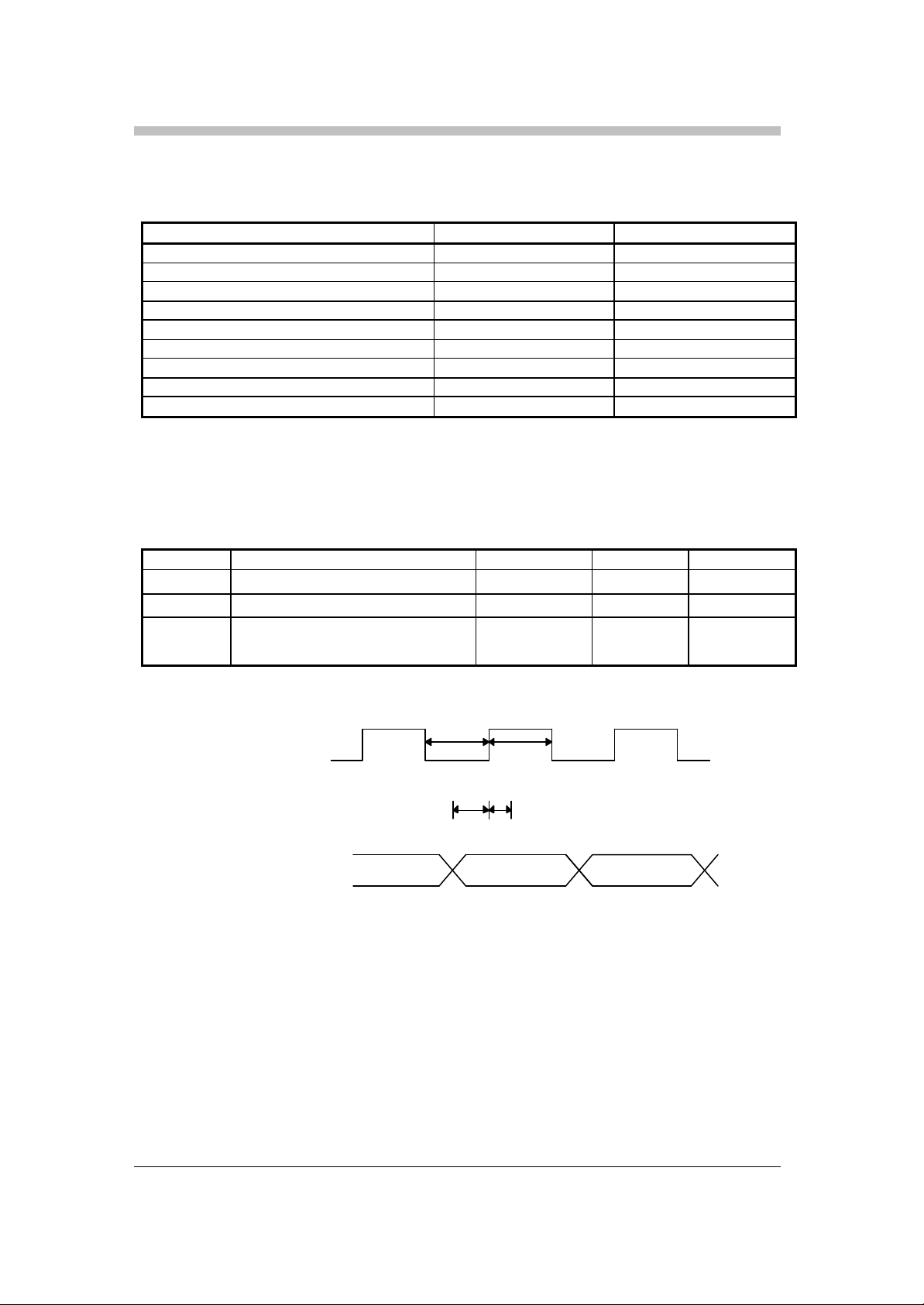
Table 3: Demodulator Specifications
Parameter Min. Max.
Sampling Clock Frequency 1MHz 75MHz
Analog Input Full Scale Range 0.9 Vpp 1.1 Vpp
Symbol Rate 1Msps 55Msps
Viterbi Data Rate - 75Mbps
Reed Solomon Data Rate - 69Mbps
Implementation Loss - 0.5 dB
Symbol Rate Resolution Clock/(220) Carrier Frequency Resolution Clock/(220) Acquisition Sweep Range - + or - Clock/2
Table 4: AC Characteristics
Symbol Parameter Min. Max. Unit
t
Input Data Setup before Clock 6 - ns
su1
th1 Input Data Hold after Clock 2 - ns
t
Low Pulse Width of Clock 8.7 - ns
pw1
t
High Pulse Width of Clock 8.1 - ns
pw2
tpw1
t
pw2
t t
su1 h1
F IGURE 2: INPUT DATA TIMING DIAGRAM
Page 11
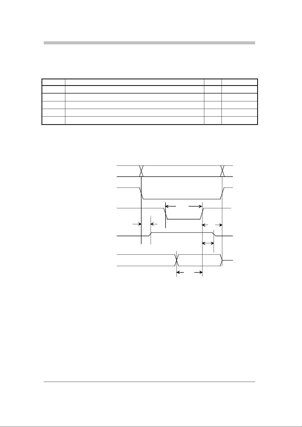
11
Valid
HI_ADDR [4:0]
/CE
/REDTACKHI_D
A
TA[7:0]
t
t
t
t
t
t
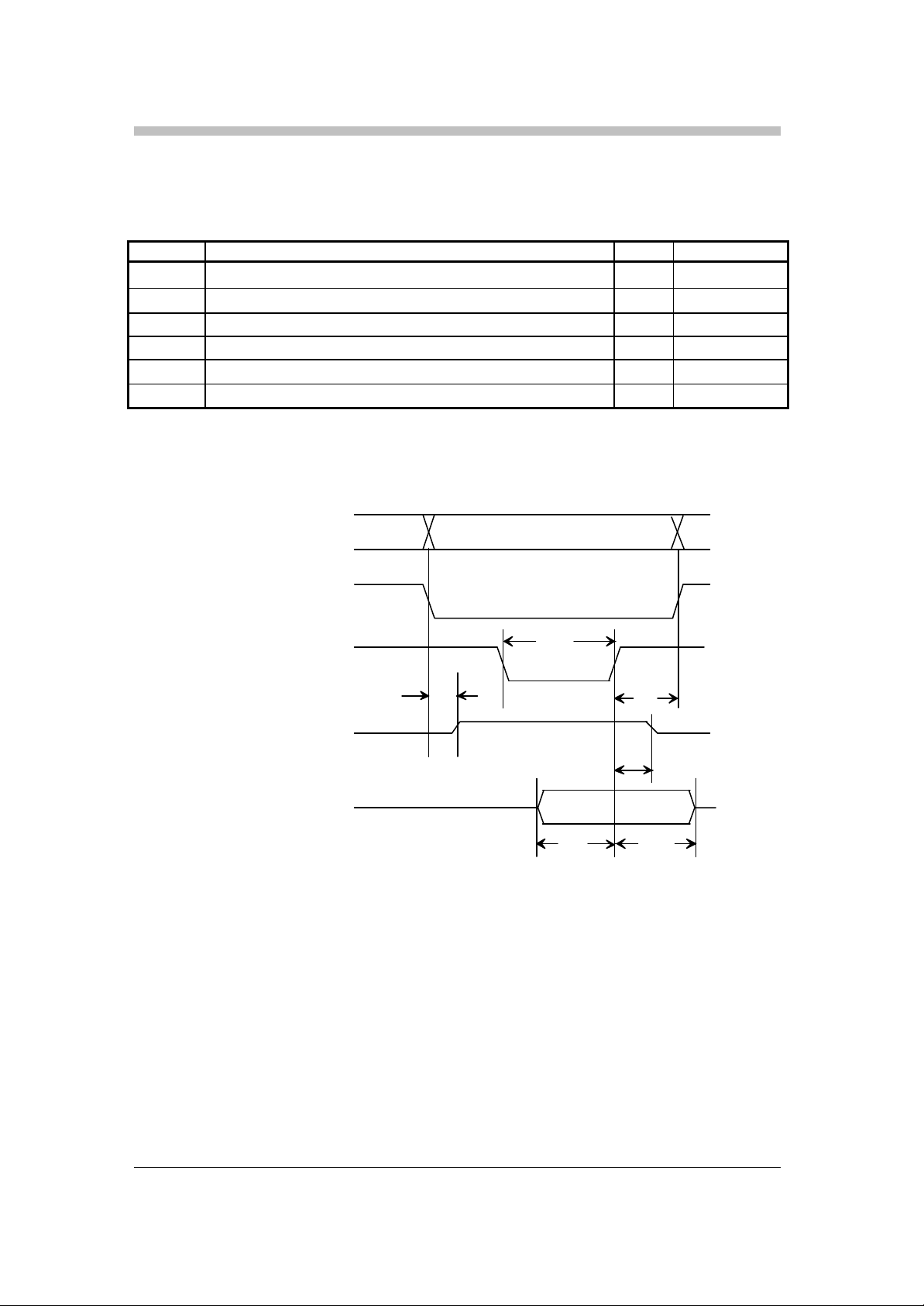
Table 5: Intel 80C88A Read Cycle Timing Parameters (Busmode = 1)
Symbol Parameter Min. Max. Unit
t
Input Address and /CE Setup before /RE Inactive 35 - ns
su1
th1 Input Address and /CE Hold after /RE Inactive 5 - ns
t
/RE Low Duration 200 - ns
pw1
td1 Delay from /CE to DTACK Active - 35 ns
t
Delay from /RE Inactive to DTACK in Tristate Mode - 10 ns
doz1
t
Delay from /RE Inactive to HI_DATA [7:0] Tristate Mode 10 - ns
doz2
pw1
d1
Z
su1
FIGURE 3: I NTEL 80C88A READ TIMING DIAGRAM
Note: HI_ADDR[4:0] is derived from the processor(80C88A) A15-A8 bus and HI_DATA[7:0] is
connected to the AD7 - AD0 bus.
#This page is only for HDM8513AP.
h1
Z
doz1
doz2
Page 12
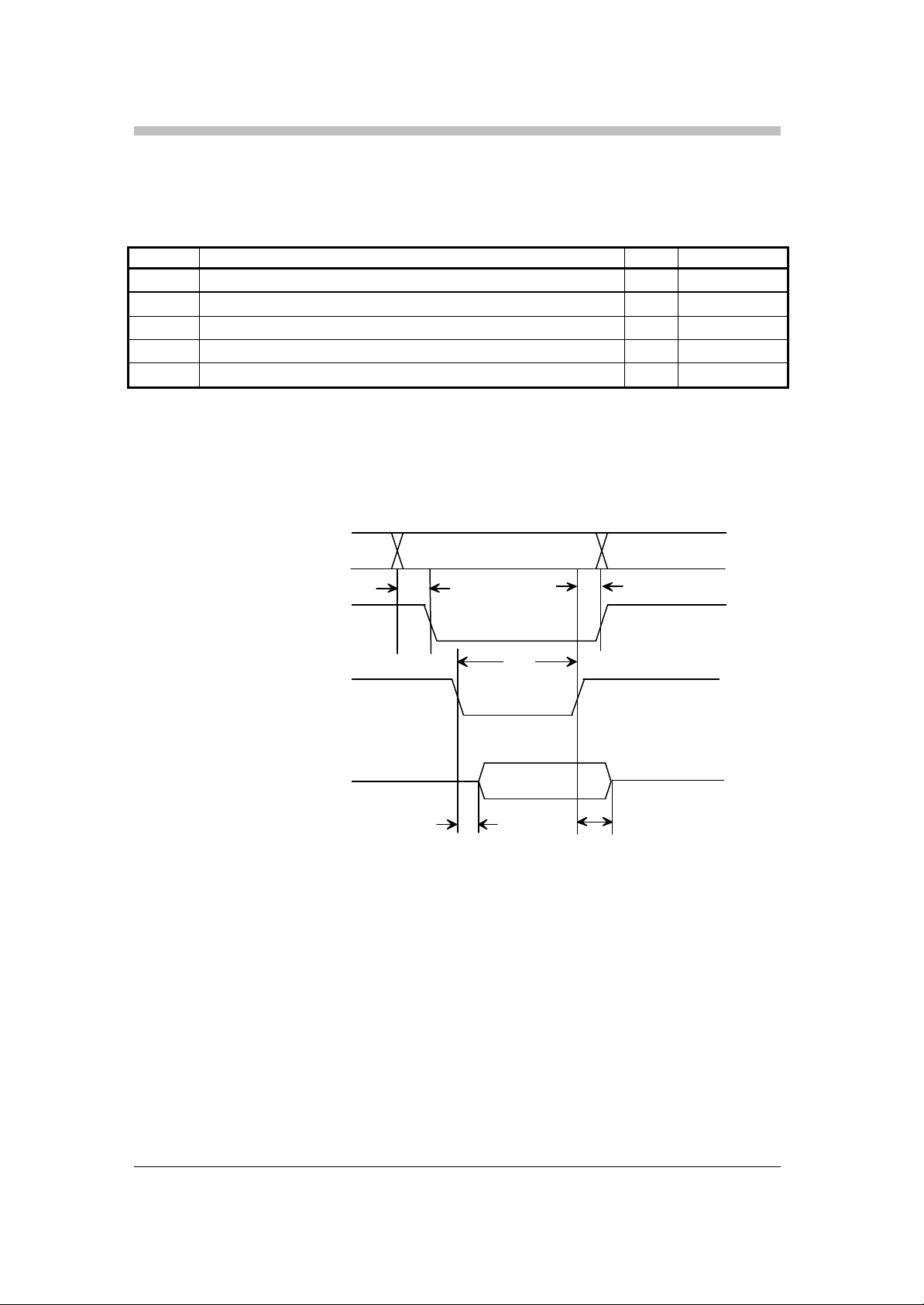
12
Valid
HI_ADDR [4:0]
/CE
/WE
DTACKHI_DATA[7:0]
th1t
t
t
t
Table 6: Intel 80C88A Write Cycle Timing Parameters (Busmode = 1)
Symbol Parameter Min. Max. Unit
t
Input Data Setup before /WE Inactive 20 - ns
su1
th1 Input Address, Data and /CE Hold after /WE Inactive 8 - ns
t
/WE Low Duration 200 - ns
pw1
td1 Delay from /CE to DTACK Active - 35 ns
t
Delay from /WE Inactive to DTACK in Tristate Mode - 15 ns
doz1
pw1
d1
doz1
su1
FIGURE 4: INTEL 80C88A WRITE TIMING DIAGRAM
Note: HI_ADDR[4:0] is derived from the processor(80C88A) A15-A8 bus and HI_DATA[7:0] is
connected to the AD7 - AD0 bus.
#This page is only for HDM8513AP.
Page 13
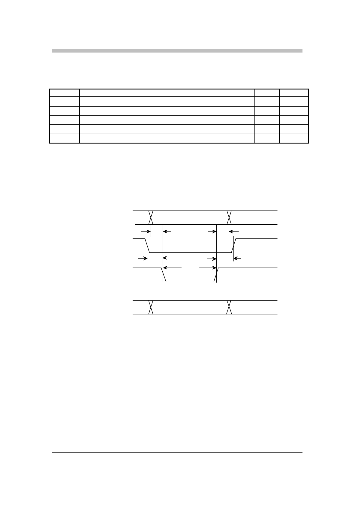
13
Valid
HI_ADDR [4:0]
/CE
/REHI_DATA[7:0]
t
t
t
t
t
Table 7: Intel 8051 Read Cycle Timing Parameters (Busmode = 1)
Symbol Parameter Min. Max. Unit
t
Input Address Setup before /CE Active 5 - ns
su1
th1 Input Address and /CE Hold after /RE Inactive 5 - ns
t
/RE Active Duration 400 - ns
pw1
t
Delay from /RE Active to HI_DATA [7:0] Valid - 40 ns
pd1
t
Delay from /RE Inactive to HI_DATA[7:0] Tristate Mode 10 - ns
doz1
FIGURE 5: I NTEL 8051 READ TIMING DIAGRAM
#This page is only for HDM8513AP.
su1
pd1
h1
pw1
doz1
Page 14
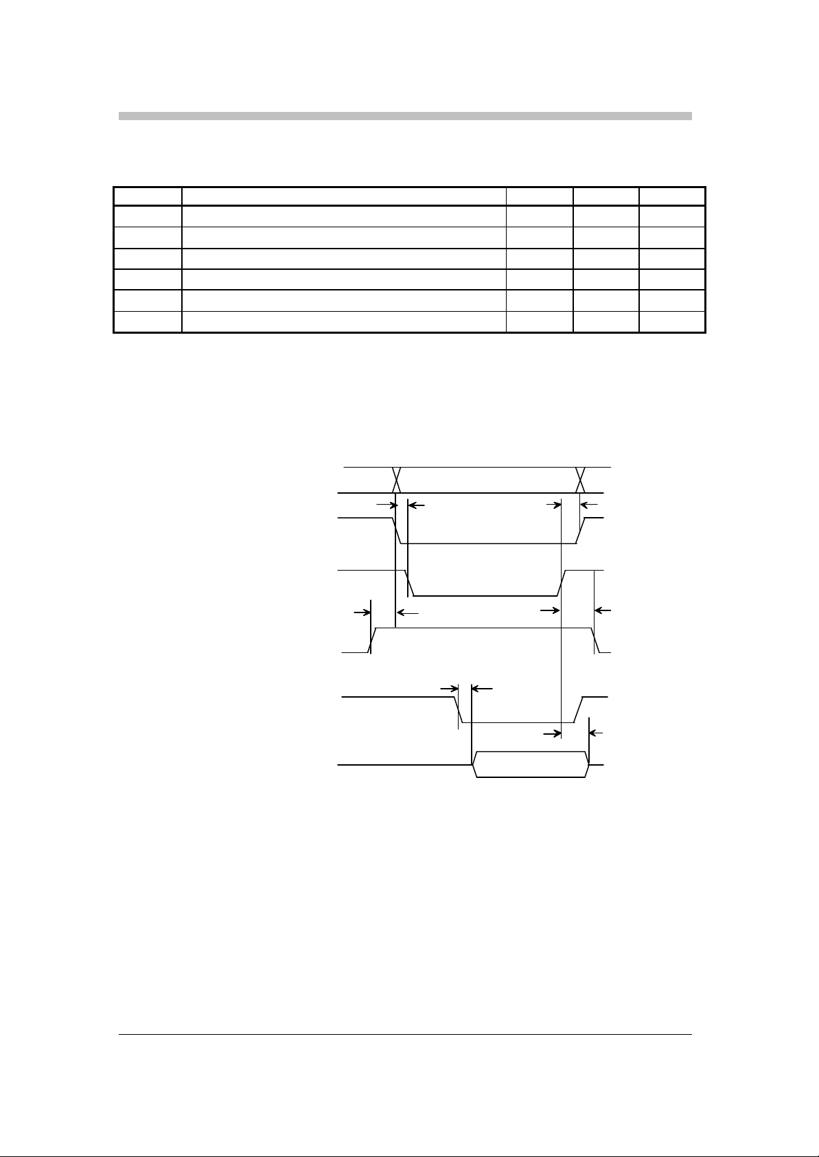
14
Valid
HI_ADDR [4:0]
/CE
/WE
HI_DATA[7:0
]
t
t
t
Valid
t
t
Table 8: Intel 8051 Write Cycle Timing Parameters (Busmode = 1)
Symbol Parameter Min. Max. Unit
t
Input Address and Data Setup before /WE Active 5 - ns
su1
th1 Input Address and Data Hold after /WE Inactive 5 - ns
t
/WE Active Duration 400 - ns
pw1
t
/CE Setup to /WE Active 5 - ns
su2
th2 /CE Hold after /WE Inactive 5 - ns
FIGURE 6: I NTEL 8051 WRITE TIMING DIAGRAM
#This page is only for HDM8513AP.
su2
su1
h1
h2
pw1
Page 15
15
Table 9: Motorola Read Cycle Timing Parameters (Busmode =0)
Symbol Parameter Min. Max. Unit
t
Setup Time of R/W with respect to /CE Active 5 - ns
su1
t
Address Setup with respect to /DS Active 5 - ns
su2
td1 Delay from DTACK Active to Data Valid - 30 ns
th1 R/W Hold with respect to /DS Inactive 5 - ns
th2 Address Hold with respect to /DS Inactive 5 - ns
th3 Data Hold with respect to /DS Inactive 10 - ns
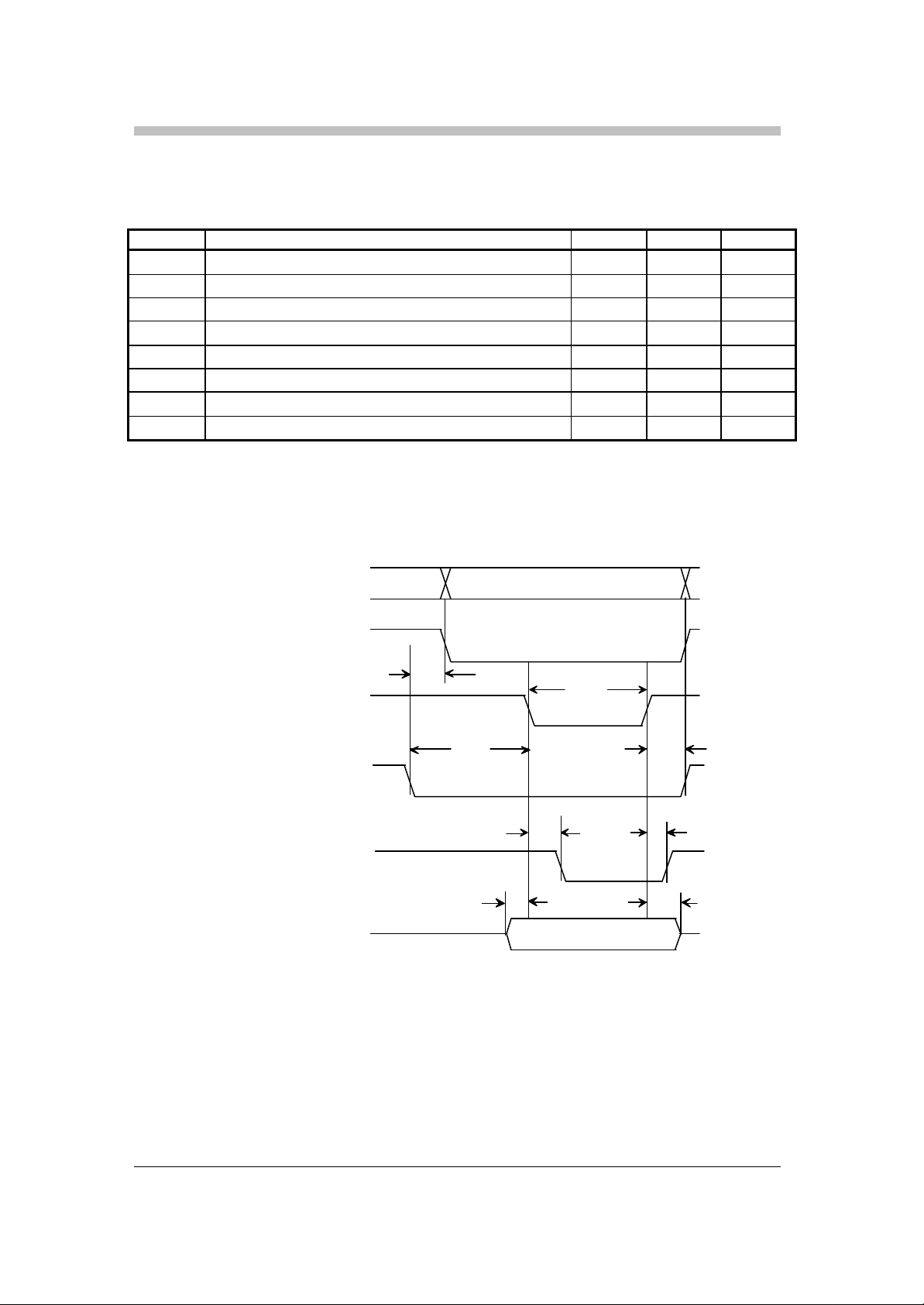
HI_ADDR[4:0]
t
su2
/CE
/DS
t
su1
R/W
DTACK
HI_DATA[7:0]
FIGURE 7: MOTOROLA READ TIMING D IAGRAM
Note: External pull-up resistor is required on DTACK.
#This page is only for HDM8513AP.
Valid
t
d1
t
h2
t
h1
t
h3
Page 16
16
/CS
/DS
HI_DATA[7:0]
t
ttt
t
Table 10: Motorola Write Cycle Timing Parameters (Busmode =0)
Symbol Parameter Min. Max. Unit
t
Data Setup to /DS Active 5 - ns
su1
t
R/W Setup to /CS and Address 3 - ns
su2
td1 /DS Delay from R/W 5 - ns
td2 DTACK Delay from /DS Active - 40 ns
td3 DTACK Delay from /DS Inactive - 10 ns
t
/DS Active Duration 5 - ns
pw1
th1 Address, /CS and R/W Hold from /DS Inactive 5 - ns
th2 Data Hold from /DS Inactive 5 - ns
HI_ADDR[4:0]
su2
d1
R/W
DTACK
t
su1
FIGURE 8: MOTOROLA WRITE TIMING D IAGRAM
Note: External pull up resistor is required on DTACK.
#This page is only for HDM8513AP.
Valid
d2
t
pw1
Valid
h1
d3
t
h2
Page 17
17
1234n
n-1
n-2
n-3xxxxxxxxxxxxxxxx
xx
12348n-5
8n-6
8n-7
8n-8xxxx
xxxx8n-4
8n-3
8n-2
8n-1
8n
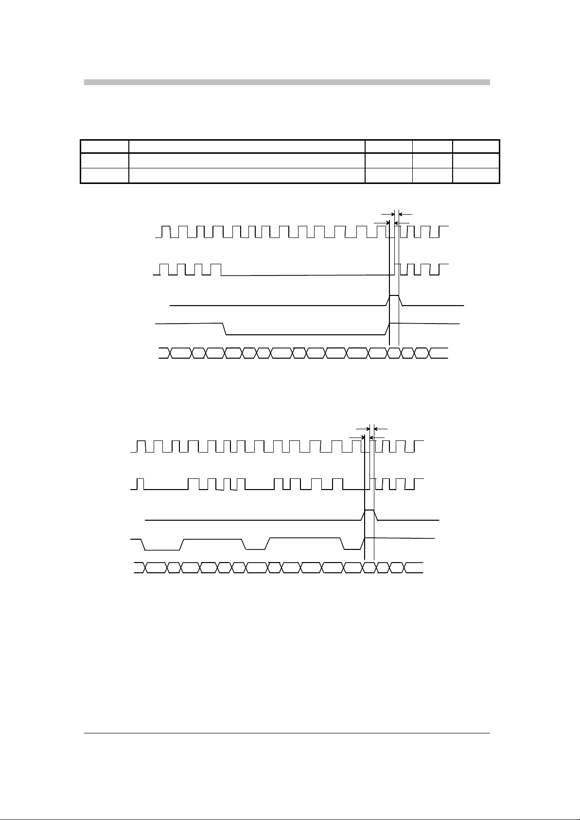
Table 11: Output Timing
Symbol Parameter Min. Max. Unit
tsu Output Data Setup before DATA_CLK and DATA_STB 5 - ns
thd Output Data Hold after DATA_CLK and DATA_STB 10 - ns
t
hd
DATA_CLK
DATA_STB
FRAME_SYNC
DATA_VALID
t
su
DATA
FIGURE 9: O UTPUT TIMING DIAGRAM FOR NORMAL PARALLEL
DATA_CLK
DATA_STB
FRAME_SYNC
DATA_VALID
DATA[0]
FIGURE 10: O UTPUT TIMING DIAGRAM FOR NORMAL SERIAL
NOTE : In case of DVB, n is 188
In case of DSS, n is 144
t
t
su
hd
Page 18
18
123
4
n-1
n-2
n-3
xxxxxxxxxxxxxxxxxxxxxxxxxxxxxx
xx
n
12348n-5
8n-6
8n-7
8n-4xxxxxxxxxxxxxxxx
xx
8n-8xxxx
8n-3
8n-2
8n-1
8n
123
4
8n-7
8n-4
8n
8n-8xxxx
xx
xxxxxxxxxxxxxx
xx
8n-5
8n-6
8n-1
8n-2
8n-3
DATA_CLK
DATA_STB
FRAME_SYNC
DATA_VALID
DATA
DATA_CLK
DATA_STB
t
su
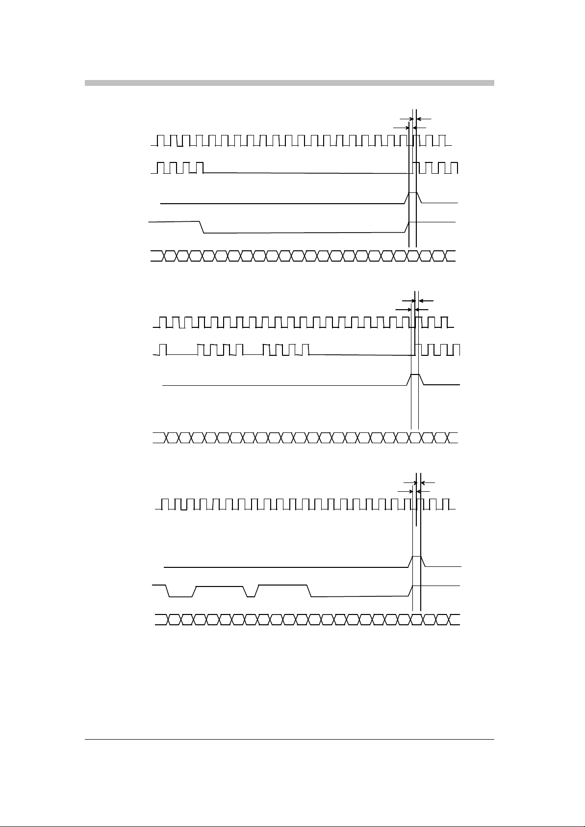
FIGURE 11 : OUTPUT TIMING DIAGRAM FOR REGULATED PARALLEL
t
su
t
hd
t
hd
FRAME_SYNC
DATA[0]
FIGURE 12: O UTPUT TIMING DIAGRAM FOR REGULATED SERIAL MODE1
DATA_CLK
FRAME_SYNC
DATA_STB
DATA[0]
FIGURE 13: O UTPUT TIMING DIAGRAM FOR REGULATED SERIAL MODE2
NOTE : In case of DVB, n is 188
In case of DSS, n is 144
t
t
su
hd
Page 19

19
3. Technical Overview
3.1 Dual Channel Analog to Digital Converter
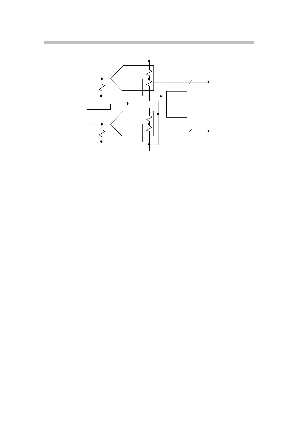
The block diagram shown below illustrates internal configuration of the Dual Channel ADC.
Baseband signals, in -phase(I) and quadrature phase(Q), which are generated by down converters,
are applied to the dual channel ADC and quantized to 6-bit digital codes respectively. The ADC is
optimized to allow AC coupled inputs with full scale input range of 1V + or - 10%. An LSB weight is
approximately 15.6 mV.
The full scale input analog conversion range (Vpp) is determined by the voltages of VTOP and
VBOT and simply equal to (VTOP - VBOT). The full scale range is defined as the voltage range that
accommodates 63 codes of equally spaced LSBs. Also the ADC supplies its own reference
voltages for A/D conversions. The voltages can be monitored by external reference pins. The
VTOP, VBOT represent top and bottom reference voltages respectively. REF_I, REF_Q represent
middle reference voltages for each channel. All these 4 reference voltage pins should be by -passed
to GND via 0.1uF capacitors. The values of internally generated voltage of VTOP and VBOT are
2.0V and 1.0V respectively. Vpp can be adjusted by externally applying voltages to both VTOP
and VBOT pins respectively when different conversion ranges are necessary. VTOP can be
adjusted as high as 2.3V and VBOT can be as low as 0.5V. A larger input range can be
established by taking VTOP higher and VBOT lower than on -chip generated voltages.
To supply necessary bias voltages for AC coupled applications, REF_I and REF_Q, which are
middle reference voltages for I and Q channel, are connected to the analog input pins (AIN_I and
AIN_Q ) respectively through 40 kohm resistors, as shown in the block diagram. For DC coupled
applications, these voltages can be used to feed back offset compensation signals.
To insure optimum performance, a low impedance analog ground plane is recommended and
should be separated from other digital ground planes. The analog power supplies should be bypassed at device to analog ground through 0.1uF ceramic capacitors.
Page 20
20
AIN_Q
VBOT
CLOCK
REF_I
REF_Q
VTOP
AIN_I
6-bit ADC
Ref.
Voltage
Gen.
6-bit ADC
FIGURE 14: ADC B LOCK DIAGRAM
6
6
DI
DQ
Page 21
21
Multiplie
r
Filters
AGC
s
s
SymbolTimingDiscriminatorSymbolTrackingLoop FilterPhase
Accumulator
SineCosin
e
CarrierTrackingLoop FilterNominal Carrier FrequencyCarrierPhaseDiscriminator
Q
o
o
LockDetecto
r
LockSweepContro
l
3.2 Variable Rate Demodulator
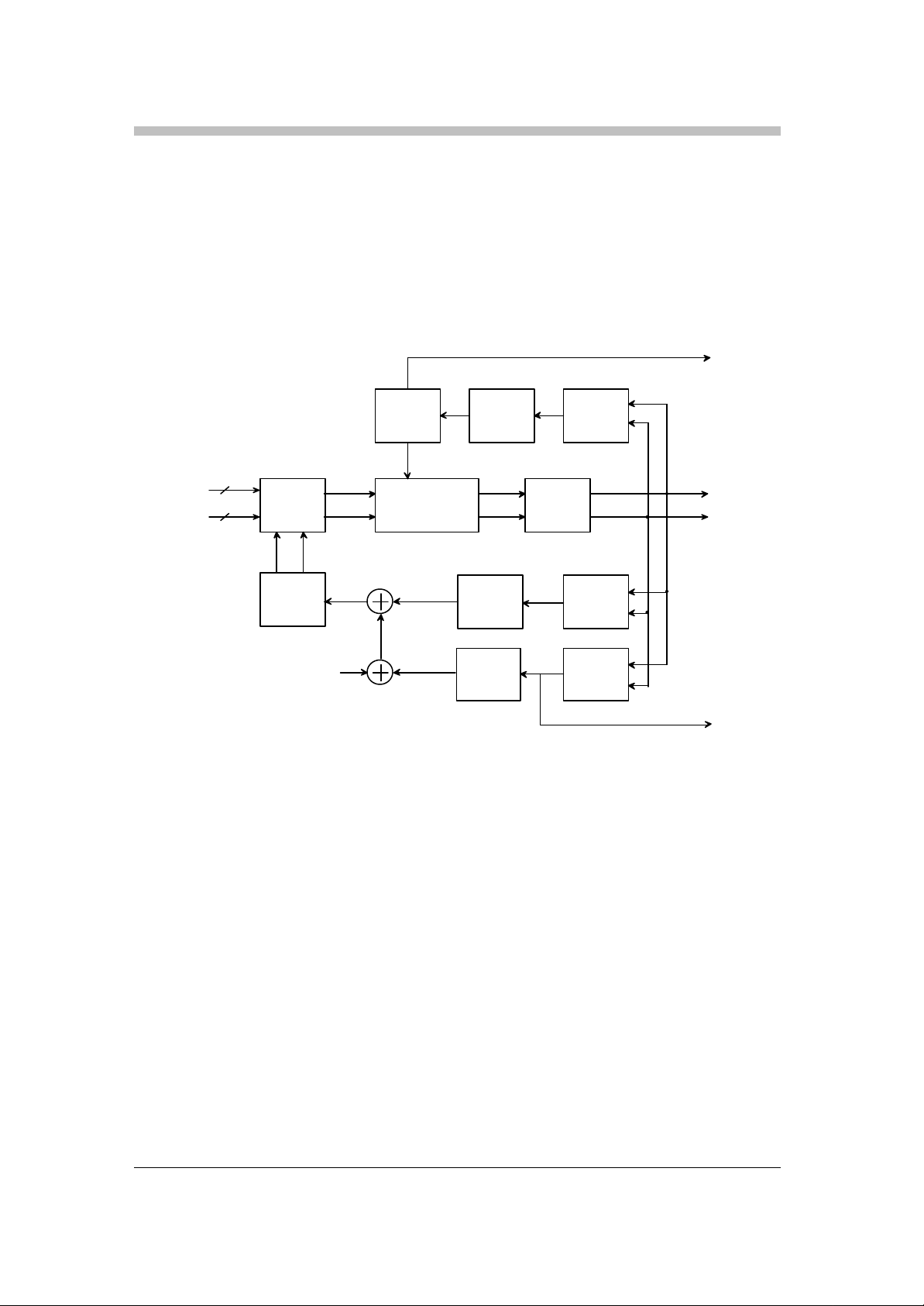
The block diagram illustrates the overall configuration of the variable rate QPSK demodulator.
Baseband in-phase (I) and qu adrature (Q) inputs are applied to the demodulator at a fixed sampling
rate. These digital samples are produced by A/D converters which employ AC coupling to minimize
DC offset.
Symbol Clock
6
I
6
Q
Complex
Polyphase
Narrowband
I
Digital
Oscillator
FIGURE 15: DEMODULATOR BLOCK DIAGRAM
The carrier frequency error associated with these samples is removed digitally during tracking
operations by a complex multiplier and a digitally controlled oscillator, sometimes called a
numerically controlled oscillator (NCO). During initial acquisition, coarse frequency error is
removed by a combination of the digital AGC within the HDM8513A and external analog tuning
circuits.
A polyphase filter performs the root raised cosine filtering of the frequency corrected baseband
samples. This filter, which implements the function of equation (1), is always configured to have an
impulse response duration of 4 symbols regardless of the programmed symbol rate. For low
symbol rates, a large number of samples are used, while for high symbol rates a relatively low
number of samples are processed for each filter output. The outputs of the polyphase filters are
applied to a digital narrowband AGC which insures that the signal is optimally scaled to the Viterbi
decoder to an accuracy of + or - 0.5 dB to insure optimum FEC performance.
y[k] = Σ h[n] x[k- n] (1)
In addition to optimizing performance of the Viterbi decoder, the digital narrowband AGC also
insures that the performance of the symbol timing and carrier tracking loops is independent of
Page 22

22
signal level variations. An analog wideband AGC is also employed to insure that the analog signal
applied to the A/D converters is properly scaled.
Both the symbol timing and carrier tracking loops are implemented digitally, which eliminates the
need for external connections to analog tuning components during steady state operation. This
causes the requirements on the analog presampling filter to be relaxed, permitting a lower cost
analog front end. For systems which require a narrowband presampling filter, and have the potential
for significant frequency error in the LNB (several MHz) the HDM8513A provides a high resolution
measure of carrier frequency to permit periodic readjustment of the front end tuner frequency to
compensate for drift. The host processor periodically reads the frequency register, then computes
appropriate correction to the tuner frequency.
The nominal symbol rate and the nominal carrier frequency are programmed into the demodulator
to an accuracy provided by 20 bits of resolution, and the system accuracy is equivalent to that of
the fixed frequency sampling clock.
During initial acquisition, the HDM8513A provides an automated sweep program to facilitate carrier
acquisition. The host processor loads a 20 bit register which determines the initia l carrier
frequency. A 16 bit register is programmed with the number of symbol times the receiver will dwell
at each frequency. If the receiver remains at the initial frequency for the programmed number of
symbol times without achieving lock, the carrier frequency is incremented by the step frequency
value programmed into another 16 bit register. If no lock is achieved, the receiver will continue to
increment the frequency until the maximum number of search frequencies, as determined by the
value in an eight bit register, is achieved. When the maximum number of search frequencies is
reached, the carrier frequency returns to the initial value and the entire process is repeated. Once
the host processor determines that lock is achieved by observing the loc k flag, it then inhibits the
sweep function and programs loop bandwidth parameters which are optimized for steady state
performance.
Page 23
23
AbsoluteValue
255256816
8
AbsoluteValue
2552568168In PhaseComponent
Average MagnitudeInstantaneousDeviation
Deviation
8168In PhaseComponent
-
3.3 Noise Measurement Circuit
When the DBS system is being installed in any place, the most difficult part of the installation is
accurate pointing of the antenna toward the satellite. Inaccurate pointing results in loss of margin
and greater potential for outages in adverse weather conditions. Existing systems use information
from the demodulator forward error correction circuits to provide a measure of antenna pointing.
Unfortunately, this method is useful over a range of only several dB above system threshold.
The HDM8513A employs a unique circuit for accurate measure of signal strength over a 20 dB
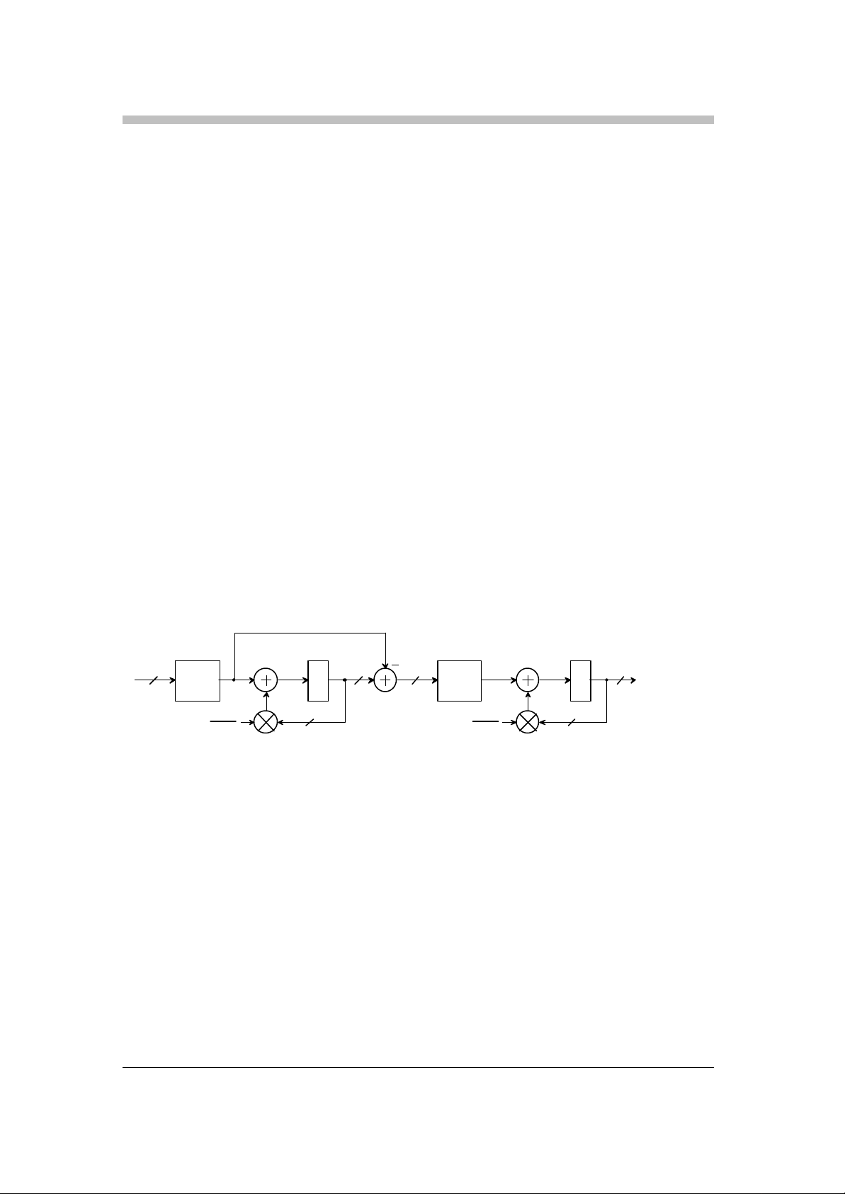
range of signal to noise ratio. This method, illustrated in the block diagram, makes use of the fact
that the demodulator provides 8 bits of resolution for each of the quadrature output components.
This high resolution provides a means of measuring the noise component with great accuracy.
The eight bit in-phase demodulator filter output is detected by an absolute value circuit, then
passed through an IIR to provide a measure of average signal amplitude. Each sample is then
subtracted from this average amplitude to provide an instantaneous noise sample. The absolute
value of these noise samples are then averaged by a second IIR to provide a measure of the noise
which is roughly proportional to the noise power and inversely proportional to signal to noise ratio.
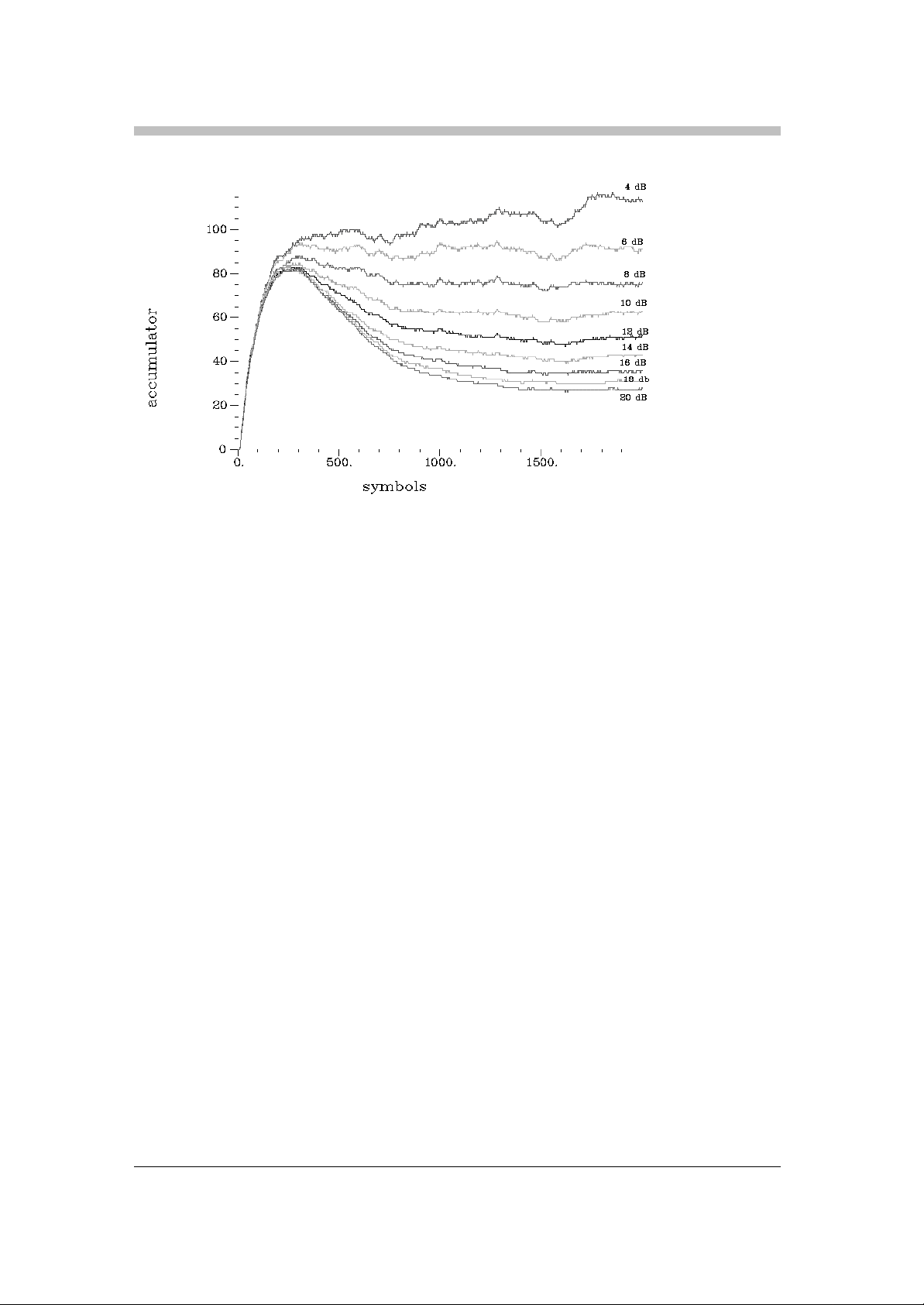
Finally, the Figure 17 illustrates the results of simulations under different noise conditions. This
figure illustrates that for signal- to-noise ratio as high as 19 dB, the noise measurement circuit
provides a meaningful measure of signal power with worst case resolution of 1 dB.
R
FIGURE 16: NOISE MEASUREMENT CIRCUIT
Average
R
Page 24
24
FIGURE 17: NOISE ACCUMULATOR AS A FUNCTION OF SNR AND TIME
Page 25
25
Trace-back
Controller
Quality
First-Out
Out
Viterbi
Clock
Depuncturing
Branch Metric
3.4 Viterbi Decoder
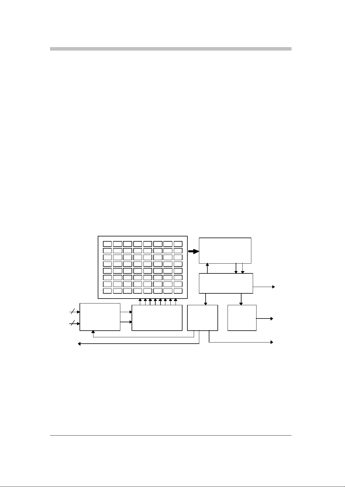
The Viterbi decoder accepts 3 bit soft decision samples of the in-phase (I) and quadrature (Q)
components of the received signal. Once QPSK lock has been achieved, the decoder searches for
the correct code rate, starting with rate 3/4, then proceeding to rate 2/3, 5/6, 7/8 and finally rate
1/2. Each of the possible synchronization phases at each rate is tested as well as the two
possible carrier phase ambiguity conditions. Polarity reversal is corrected in the word
synchronization logic. Viterbi lock is achieved when the trellis traceback algorithm converges, on
the average, within a prescribed number of symbols.
Although the algorithm automatically tests for carrier phase ambiguity, there is no provision to
automatically correct for phase reversal. Phase reversal can occur if the receiver chain, consisting
of an LNB and the tuner, provides an odd number of high side frequency translation operations. A
system may be required to operate with different LNBs, some of which provide phase reversal.
This condition may be corrected by the host processor, which can set a bit in the down converter
to correct for phase reversal.
The Viterbi decoder employs the radix two algorithm. The output buffer reserializes the data which
is made available, along with the Viterbi data clock as external signals. These signals permi t
verification of the DVB specification which is referenced to the Viterbi decoder output.
ACS Array
128
RAM
Traceback Memory
3
I
3
Q
Logic
Change Carrier Phase
G1
G2
Change Puncture Phase
Calculator
F IGURE 18: VITERBI DECODER
Decoder
Estimate
Last-In
Buffer
Out
Data
Lock
Page 26

26
3.5 Autonomous Acquisition
The HDM8513A provides several features to permit signal acquistion wi th minimal interaction with
the host microcontroller. The host microcontroller must configure the HDM8513A for a specific
symbol rate, carrier frequency, carrier sweep conditions, and tracking loop bandwidth. The
microcontroller also must monitor lock status to determine when acquisition is achieved. There are
many provisions in the HDM8513A to enable the system designer to implement custom algorithms
for specific requirements.
The microcontroller first must set the lower edge of the carrier search range in the Carrier
Frequency registers (04, 05 and 06). Then the processor configures the Carrier Sweep Step Size
register (09, 0A) to a value which is less than two times the carrier pull -in range. The number of
symbols per dwell is defined in registers (0B,0C), and is typically set to a value of 500 to 1000.
The total search range is set by the Number of Search Frequencies as defined in register 0D. The
total sweep frequency range is this number times the Carrier Sweep Step Size. The sweep
process stops once QPSK carrier lock is detected. If no lock is detected, the sweep process
continuously repeats.
The QPSK demodulator may lock to any one of four different phase reference states, only one of
which produces true I and Q data as it was modulated at the transmitter. If the local phase
reference is plus 90 degrees or minus 90 degrees with respect to the true phase, the information
provided to the Viterbi decoder will be unintelligible. If the Viterbi decoder is unable to achieve valid
lock, it will reattempt lock with a 90 degree phase shift, without external intervention.
In the event that the local phase is 180 degrees from the true phase, the data provided to the
Viterbi decoder will be inverted, but otherwise valid. The code employed by the Viterbi decoder is
transparent, thus the data from the Viterbi decoder will be inverted if the input is inverted. This
situation is corrected in the word synchronization circuit. This circuit searches for the
unscrambled sync word which occurs once per frame (every 204 bytes at the Viterbi output). Once
correlation with the sync word is found, the data is reformatted as a series of bytes with the
beginning of each 204 byte frame identified to provide the synchronization information required for
the deinterleaver and the Reed Solomon decoder. If the polarity of the sync word is incorrect, the
data is inverted before further processing without external interaction.
The HDM8513A supports five different code rates, including 1/2, 2/3, 3/4, 5/6 and 7/8. When rate
1/2 is employed, there is a one-to-one correspondence between incoming I and Q samples and G1
and G2 terms required by the Viterbi decoder. The higher rates employ punctured coding
techniques which periodically cause either a G1 or G2 term to be deleted. The puncturing pattern
can have 6 possible ambiguity states for rate 2/3, 4 states for rate 3/4, 6 states for rate 5/6 and 8
states for rate 7/8. As part of the Viterbi decoding acquisition process, each puncturing state of
each code must be tested. Total acquisition requires search of 26 different conditions. The
process starts with rate 3/4 coding and proceeds sequentially to rate 2/3, 5/6, 7/8, and finally rate
1/2.
In some systems, it may be possible to experience spectral inversion. This might occur when
different combinations of LNBs and tuners are employed which implement different frequency
translation schemes. Correction of spectral inversion must be corrected with host processor
interaction. If the host processor detects that QPSK lock is achieved, but Viterbi lock has not
occurred within a specified time, then a bit must be set in the demodulator which reverses the
spectrum.
Page 27
27
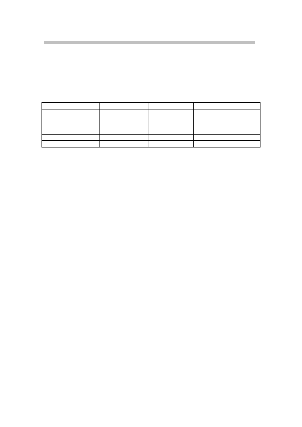
The table below illustrates a typical acquisition timing. For this example, the symbol rate is one
half of the clock rate. The code rate is set to 5/6, which requires 13 trial and errors before node
sync is achieved. The carrier search logic requires 10 dwells at different frequencies (500 symbols
per dwell) before demodulator lock is achieved.
Table 12: Example of Acquisition Timing
Bit Times Symbols Clock Cycles
Carrier Search 8,333 5,000 10,000
Viterbi Node Sync 2,652 1,591 3,182
Byte Sync 16,000 9,600 19,200
Deinterleaver Flush 19,584 11,750 23,500
Reed Solomon 1,632 979 1,958
Total Timing 48,201 26,950 57,840
The total time required for acquisition could vary widely, depending upon the carrier search range
and the time required for Viterbi node sync. For this example, however, the Byte Sync time and
the time required to flush the deinterleaver dominates the total time. If a 60MHz clock were
employed, the total acquisition time would be 0.963 milliseconds for this example
Page 28
28
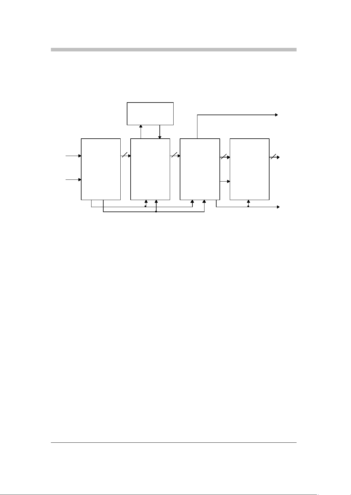
3.6 Reed Solomon Decoder
The serial output from the Viterbi is provided to the Word Sync circuits which searches for the eight
bit frame sync word which occurs every 204 bytes. By detecting the polarity of the sync word, this
module can correct polarity reversals in the data provided by the Viterbi decoder.
Byte serial data is provided to the convolutional deinterleaver, which reorders the received symbols.
This process causes errors, which typically occur in bursts from the Viterbi decoder, to be
distributed randomly over many blocks. This deinterleaved data is then provided to the Reed
Solomon decoder which can reduce an error rate of 2 x10⁻⁴ from the Viterbi decoder to less than 1
-10
in 10
. The Reed Solomon decoder accepts input data in blocks of 204 bytes and produces error
corrected blocks of 188 bytes. Maximum 8 bytes per a RS block can be corrected in RS decoder.
Reedsolomon block includes on-chip BER calculator at the output of Viterbi to monitor signal
quality or estimate the SNR of incoming signal. The calculated value can be read by accessing two
read registers via utility bus such as I2C. It represents the number of errors among 220 data bits.
The next process is descrambling, not to be confused with the descrambling which is part of
conditional access. The purpose of scrambling the transmitted data and performing the inverse in
the receiver is to insure that the spectrum of the transmitted waveform is always evenly distributed
without significant discrete spectral lines. Without the scrambling/descrambling process, a
transmitted sequence of all ones or all zeroes would result in strong spectral components and
could interfere with other signals in the same satellite transponder.
The final process is data regulation. Viterbi Data and Viterbi Clock occur irregularly according to
the code rate. Data clock regulation makes it possible to interface with external common interface
devices. To make external bus interface more flexible, interface mode such as parallel or serial can
be selected by mode selection register.
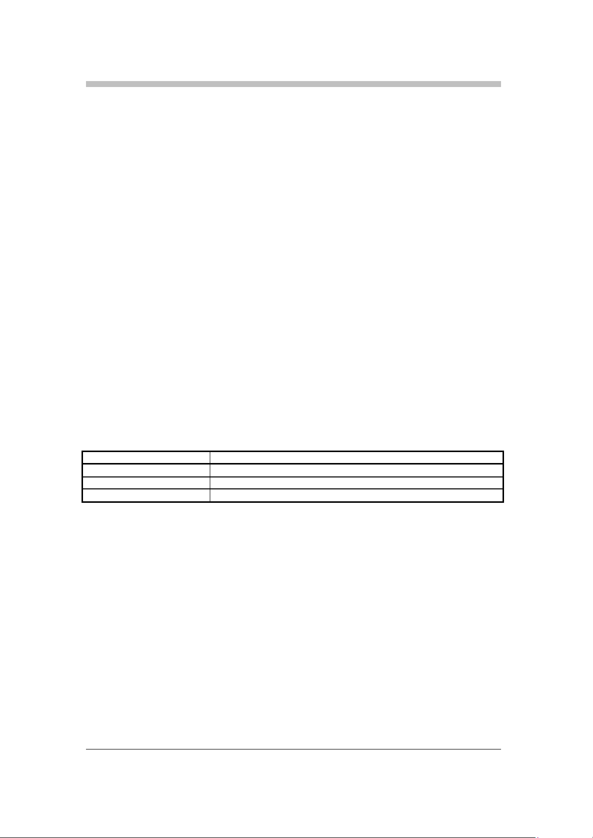
Parameter Register
Regulate_data_clk Bit 5 of 14H register
Serial_valid Bit 6 of 14H register
Mode_serial Bit 0 of 18H register
l NORMAL INTERFACE MODE (parallel/serial)
If regulate_data_clk is reset, both parallel interface and serial interface work in normal
operation which is same as HDM8513 regardless of serial_valid bit. Parallel interface or serial
interface can be alternated by modifying mode_serial bit (Refer to Figure 9 and Figure 10)
l REGULATED INTERFACE MODE (parallel)
If regulate_data_clk is set,all interfaces are from internal FIFO designed to regulate irregular
interface signals. Data clock cycle is a little bit faster than the average of cycle of irregular data
clock, so meaningless data can be output in invalid data period. (Refer to Figure 11)
l REGULATED INTERFACE MODE (serial)
If mode_serial bit is set in the regulate interface mode, regulate interface mode is enabled for
serial interface. Regular serial interface mode has two modes for more flexibility. The mode
selection is controlled by serial_valid bit. If serial_valid is reset, DATA_STB signal alternates
when every valid bit is out (mode1). While serial_valid is set, DATA_STB signal sustains high
when valid bit is out (mode2). (Refer to Figure 12 and Figure 13)
Page 29
29
Out
Data Clock
Deinterleaver
Error Flag
Memory
Viterbi
Data
Viterbi
Clock
Word
Sync.
Deinterleaver
Memory
Control
Word Clock
Frame Clock
88
Reed
Solomon
Decoder
8 8
Descrambler
Sync.
Data
FIGURE 19: REED SOLOMON DECODER
Page 30
30
fext_clk
=
f
int_clk
fint_clk
=
fext_clk
fext_clk.
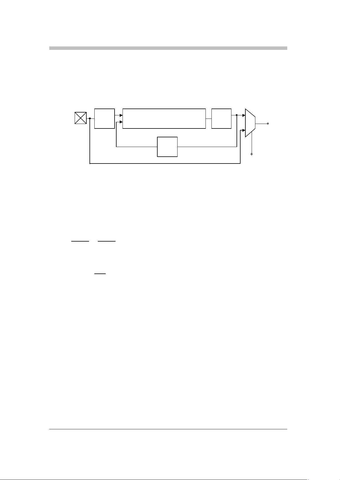
3.7 Clock Generation PLL
An integrated VCO is locked to MxN times a reference frequency provided by a external clock.
F
N
Ref
PLL Analog Core
F
Fb
Feedback
Divider
1/N
F IGURE 20: CLOCK SIGNAL GENERATION
1/2
and FFb,
Ref
1
0
enable
int_clk
ext_clk
Reference
Divider
1/M
This programmable PLL consists of a PLL analog core, a reference divider with a divider ratio M, a
feedback divider with a divider ratio N, and a divider which askes the duty cycle 1/2.
Reference divider and feedback divider are used to synthesize various frequencies from a reference
frequency,
Since PLL synchronizes the frequency and phase of two signals, F
Internal clock is calculated as fo llows
The following two PLL modes are provided to control PLL.
(1) PLL Enable mode : The internal clock is connected to the generated clock of the PLL.
(2) PLL Disable mode : The PLL is bypassed and the external clock is directly connected to the
internal clock.
More information can be found on the part of the write register.
M
N
M
Page 31
31
MC68306(MC68340)Host ProcessorL-BandTuner
480
MHzDown-
Coarse
Tuning
Step
Frequency Contro
l
Low
Filte
r
SL171
0
Seria
l
BSFC77GV6
8
Access
Interface
AGC
2
1
Fixed
Frequency PLL Contro
l
3IFI
MPEG-2
Demultiplexer
DRAM
Video
3.8 DBS Receiver
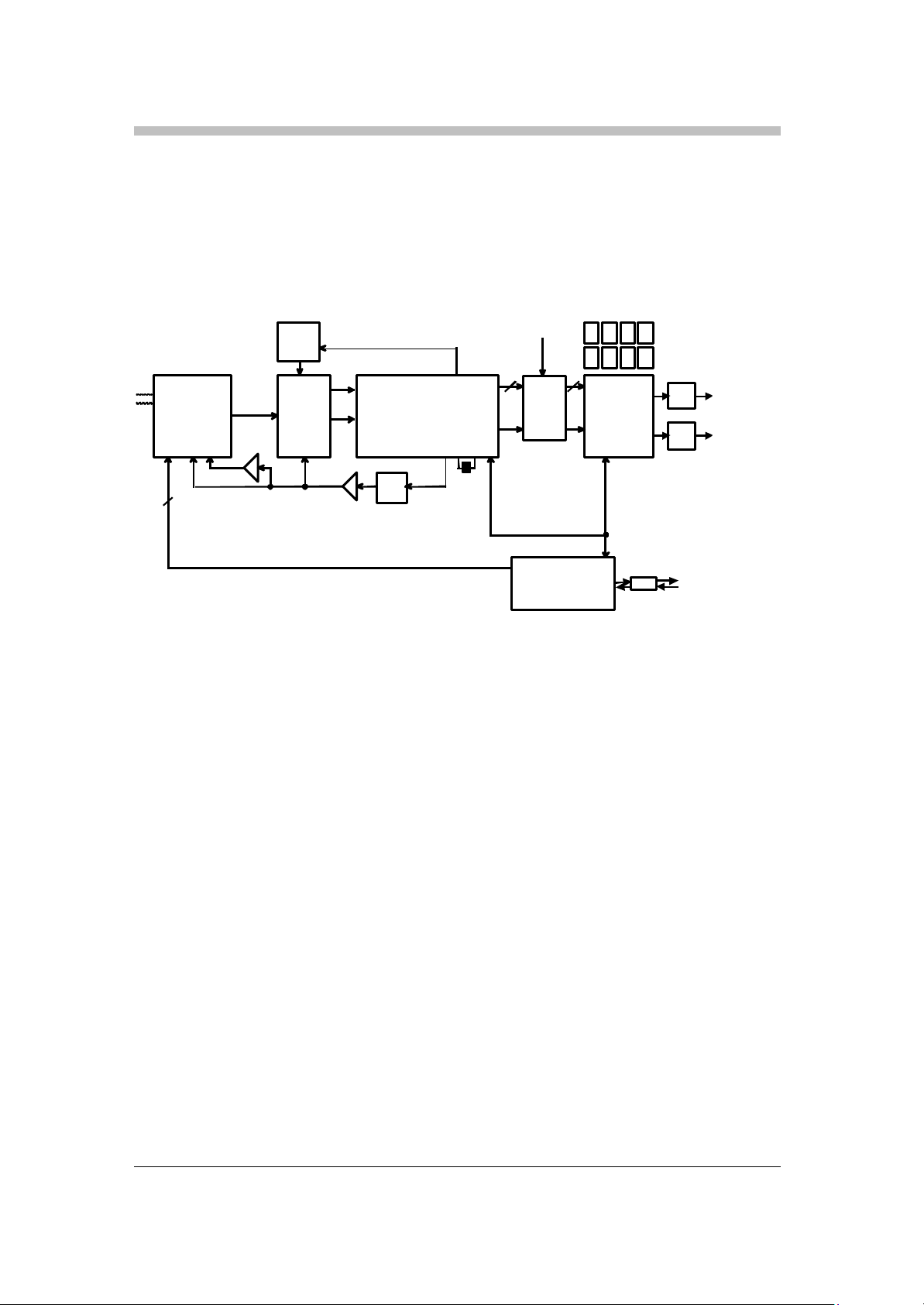
The HDM8513A DVB Demodulator including a dual A/D converter and the MPEG-2 decoder provide
the core digital processing technology for a DBS receiver conforming with the DVB standard.
480
MHz
Loop
Data
8
converter
Q
HDM8513 A
Clock
Conditional
Audio
AGC
Pass
Filter
WB
AGC
Interf ace
F IGURE 21: TYPICAL SET TOP BOX DEMODULATOR
A tuner accepts an L-band RF input from the antenna/LNB assembly located outside the building.
A host processor controls the tuner to the nominal center frequency of the target signal. Baseband
I and Q outputs from the downconverter are applied to an A/D converter pair which is sampled at a
fixed rate, 60MHz as illustrated in this exam ple. The tuner is required to filter the received
baseband signal to a bandwidth less than half the sampling rate, but is not required to perform
matched filtering.
Once the HDM8513A has locked to the target signal, the host processor may read the internal
registers to determine the steady state frequency error. This error would be used to make period
corrections to the programmed frequency of the tuner PLL.
The HDM8513A provides an output which can be used to control the analog AGC in the tuner. This
digital signal must be filtered and amplified before applying it to the AGC control element. When
the loop is closed, the signal applied to the A/D converters is optimally scaled.
Page 32
32
4. Mechanical Specifications
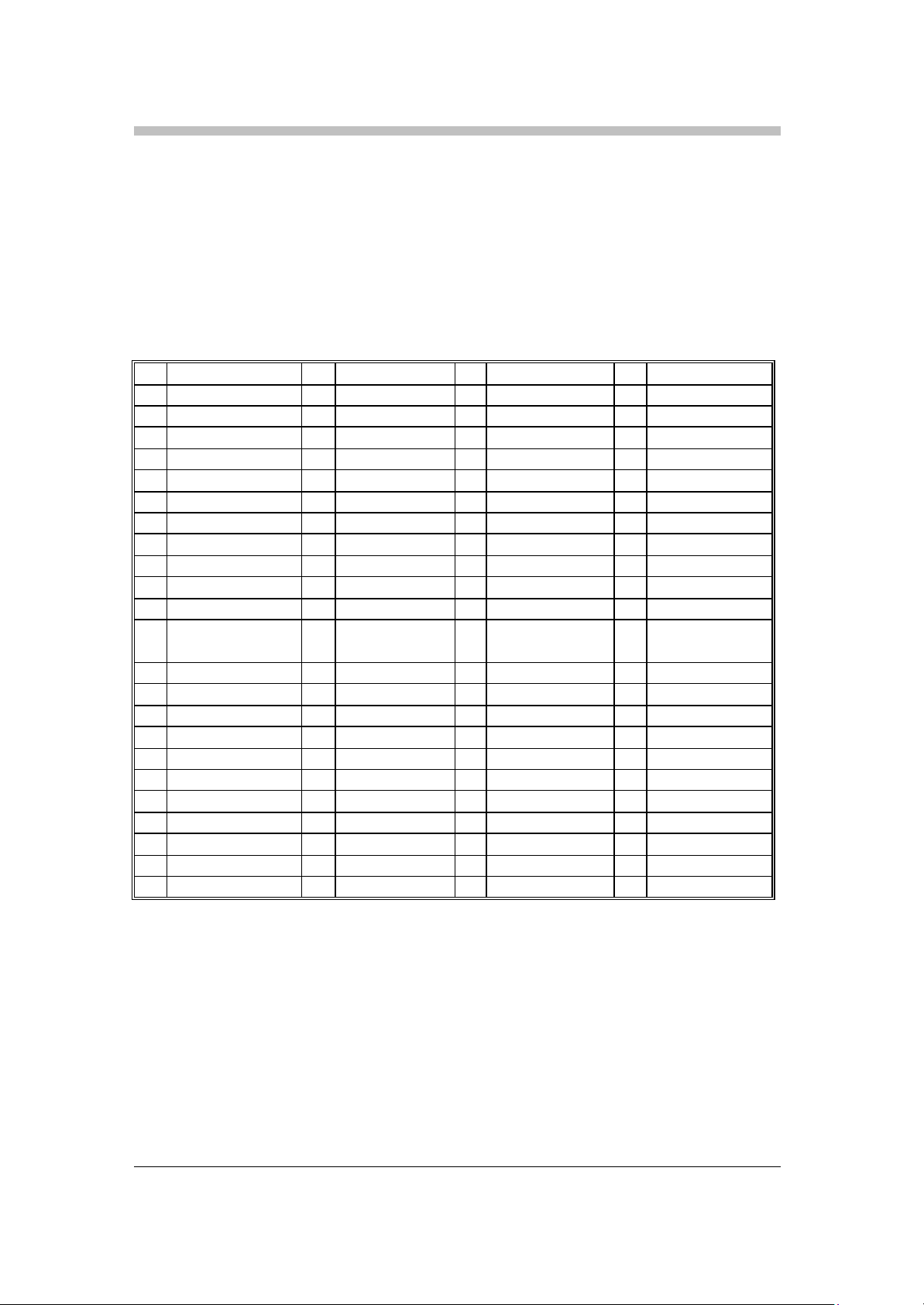
4.1 100 Pin Quad Flat Pack
4.1.1 Pin Assignment
1 DATA_CLK 26 TEST6 51 HI_ADDR4 76 DTACK
2 FRAME_ERROR 27 VDDA 52 HI_ADDR3 77 SDA_I2CO
3 FRAME_SYNC 28 VSSA 53 HI_ADDR2 78 SDA_I2C
4 VDD 29 VTOP 54 HI_ADDR1 79 SCL_I2CO
5 VSS 30 AIN_I 55 HI_ADDR0 80 SCL_I2C
6 LNB_TONE 31 VSSA 56 VDD 81 IOVDD
7 SIGMADELTA 32 VDDA 57 VSS 82 IOVSS
8 SYMBOL_CLOCK 33 REF_I 58 HI_DATA7 83 R/W(/RE)
9 WB_AGC 34 REF_Q 59 HI_DATA6 84 /CE
10 QPSK_LOCK 35 AIN_Q 60 HI_DATA5 85 /DS(/WE)
11 IOVDD 36 VBOT 61 HI_DATA4 86 VDD
12 IOVSS 37 VSS 62 IOVDD 87 VSS
13 TEST15 38 TEST5 63 IOVSS 88 DATA7
14 TEST14 39 TEST4 64 HI_DATA3 89 DATA6
15 TEST13 40 TEST3 65 HI_DATA2 90 DATA5
16 TEST12 41 VDDP 66 HI_DATA1 91 LOCK
17 VDD 42 VSSP 67 HI_DATA0 92 DATA4
18 VSS 43 TEST2 68 VDD 93 DATA3
19 TEST11 44 TEST1 69 VSS 94 IOVDD
20 TEST10 45 TEST0 70 VB_NODESYNC 95 IOVSS
21 TEST9 46 XTAL1 71 VB_CLOCK 96 DATA2
22 TEST8 47 CLOCK 72 VB_DATA 97 DATA1
23 IOVDD 48 IOVDD 73 VDD 98 DATA0
24 IOVSS 49 IOVSS 74 VSS 99 DATA_VALID
25 TEST7 50 RESET 75 BUSMODE 100 DATA_STB
Page 33
33
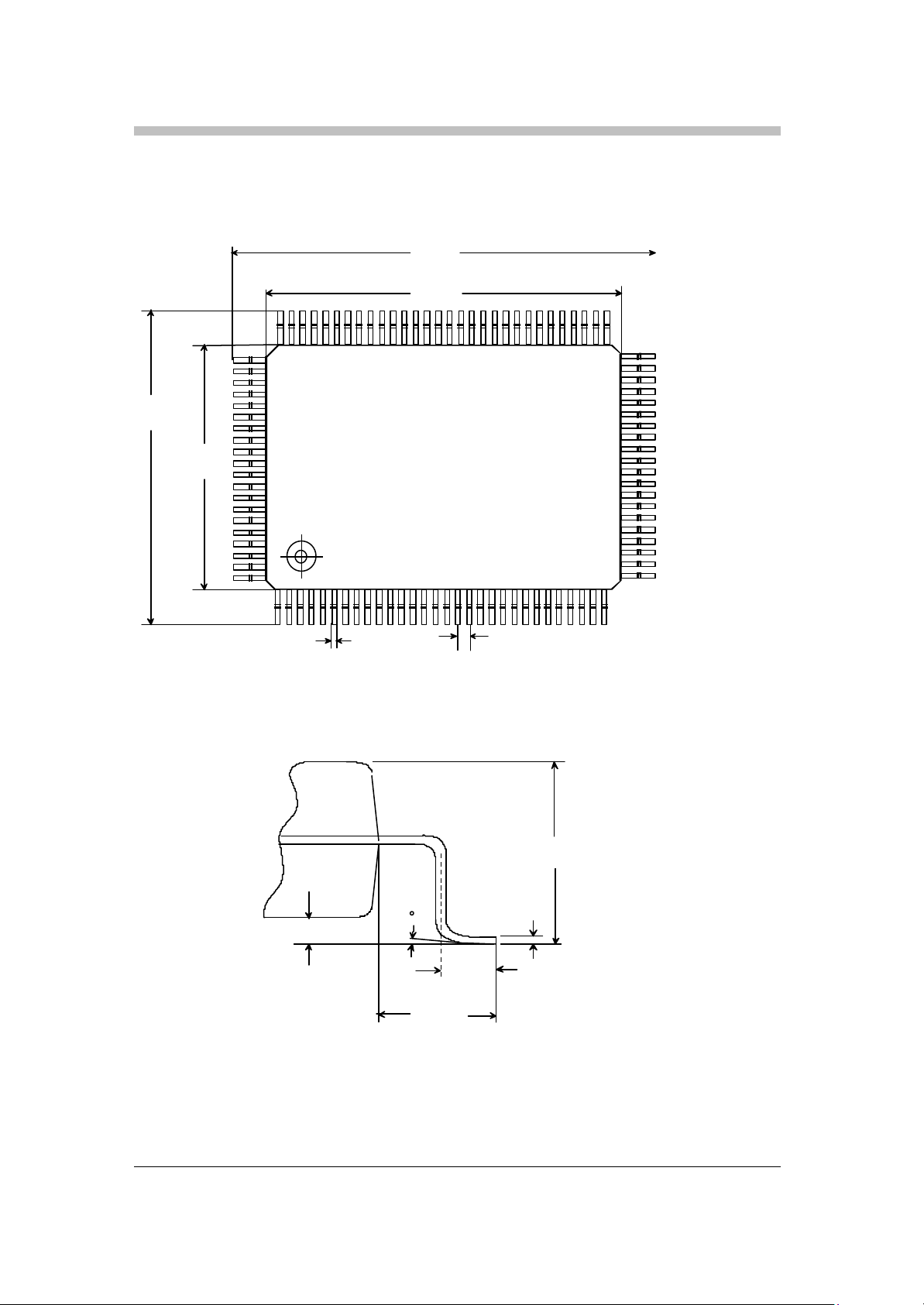
4.1.2 Package Dimensions
0.650 Typ.
DVB Demodulator
80
23.340
23.090
20.100
19.900
51
81
17.880
17.908
HDM8513A
14.100
13.900
100
0.380
All Dimensions in mm
50
31
301
0.7
0.500
0.250
1.950 Typ.
0.230
0.130
FIGURE 22: MECHANICAL CONFIGURATION
0.950
0.650
3.350
3.000
Page 34
34
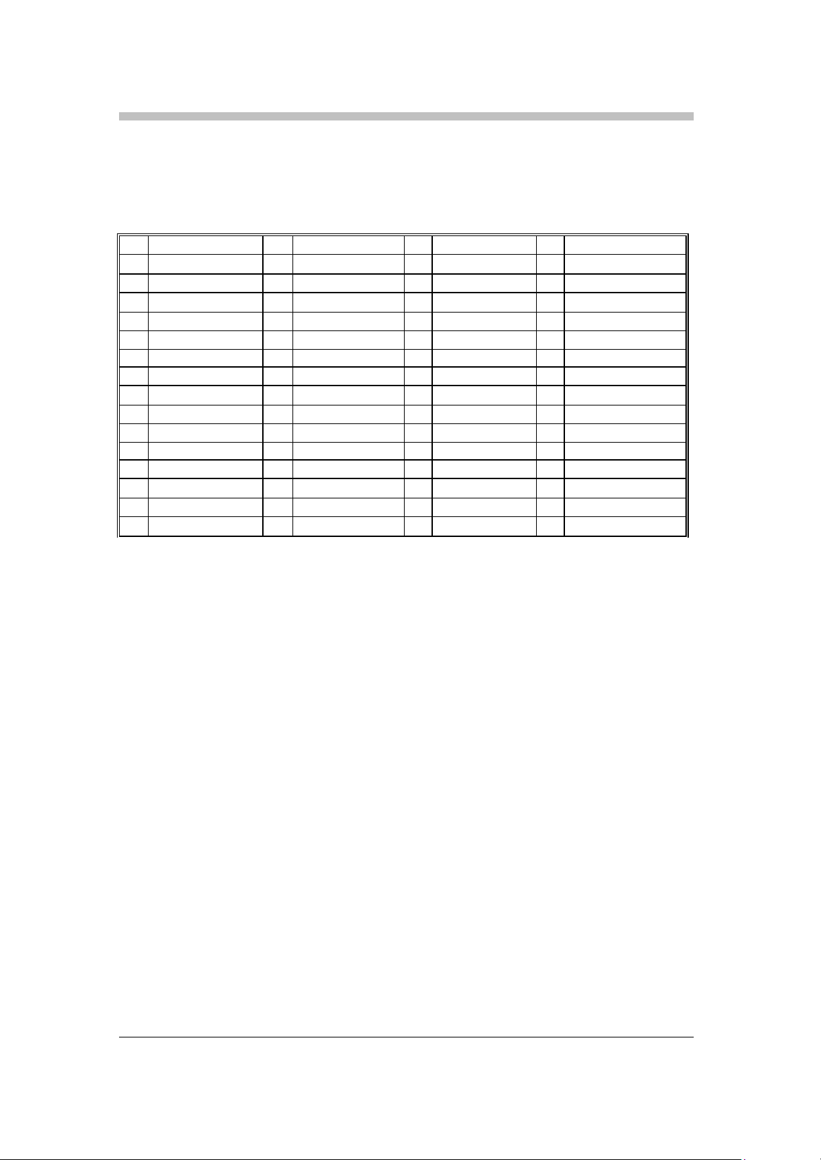
4.2 64 Pin Thin Quad Flat Pack
4.2.1 Pin Assignment
1 FRAME_ERROR 17 VSSA 33 VDD 49 IOVSS
2 FRAME_SYNC 18 VDDA 34 VSS 50 VDD
3 LNB_SYNC 19 REF_I 35 I2C_ADD2 51 VSS
4 WB_AGC 20 REF_Q 36 IOVDD 52 DATA7
5 IOVDD 21 AIN_Q 37 IOVSS 53 DATA6
6 IOVSS 22 VBOT 38 I2C_ADD1 54 DATA5
7 TEST13 23 VSSA 39 I2C_ADD0 55 LOCK
8 TEST12 24 VDD 40 VDD 56 DATA4
9 VDD 25 VSS 41 VSS 57 DATA3
10 VSS 26 N/C 42 VB_CLOCK 58 IOVDD
11 TEST11 27 N/C 43 VB_DATA 59 DATA2
12 TEST10 28 N/C 44 BUSMODE 60 DATA1
13 TEST9 29 XTAL1 45 SDA_I2C0 61 DATA0
14 TEST8 30 IOVDD 46 SDA_I2C 62 DATA_VALID
15 VTOP 31 IOVSS 47 SCL_I2C0 63 DATA_STB
16 AIN_I 32 RESET 48 SCL_I2C 64 DATA_CLK
Page 35
35
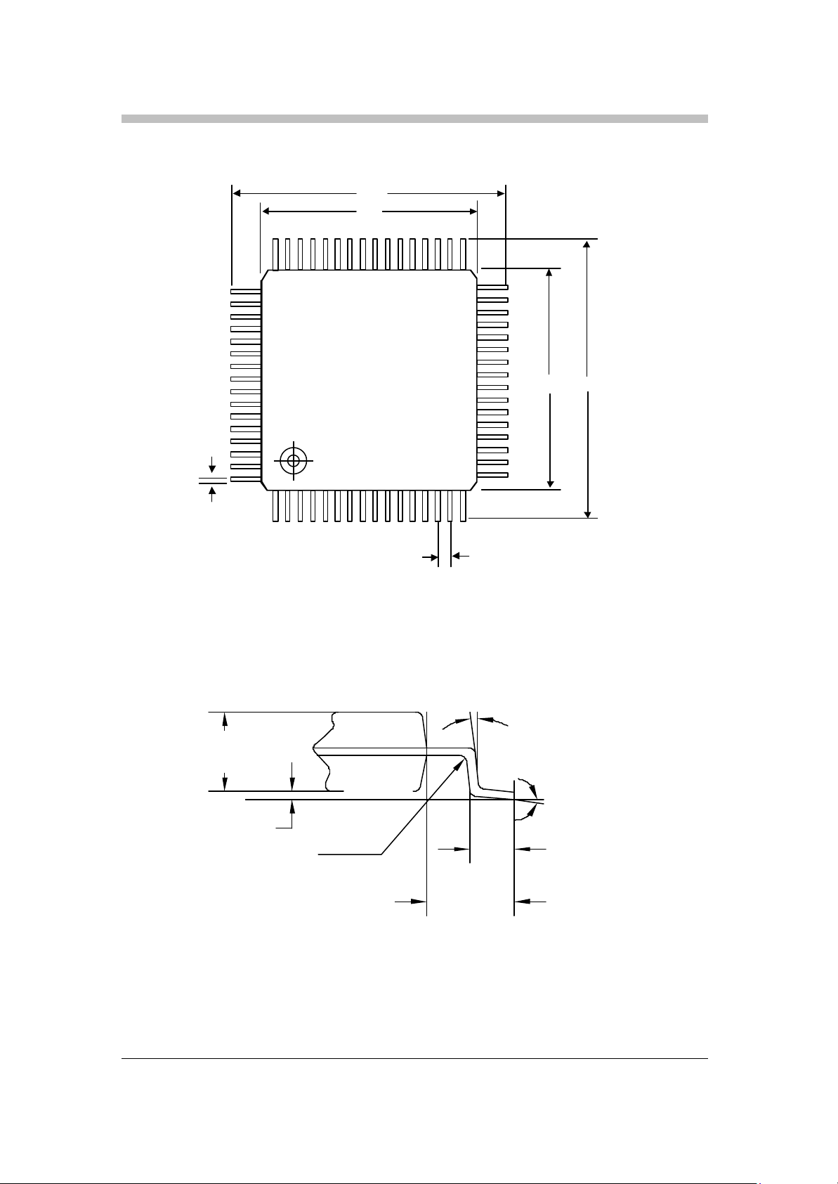
4.2.2 Package Dimensions
HDM8513AT
116173233
64
10.00
12.00
10.00
0.17 Min.
49
0.27 Max.
12.00
48
0.50
All Dimensions in mm
0 Min.
0.95 Min.
1.00 Typ.
1.05 Max.
0.15 Max.
0.08R Min.
FIGURE 23: MECHANICAL CONFIGURATION
0-7
0.45 Min.
1.00 Ref.
Page 36
36
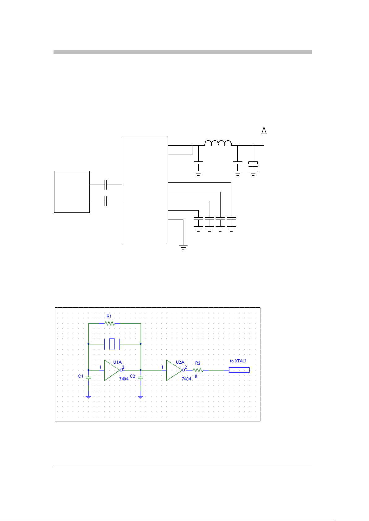
4.3 Recommended Analog Pin Connection
0.1uF
0.1uF
Down
Converter
I
Q
0.1uF 0.1uF
HDM8513A
FIGURE 24: ANALOG PIN CONNECTION
4.4 Recommended Clock Generation Circuit
(to HDM8513A)
FIGURE 25: CLOCK GENERATION CIRCUIT
Page 37

37
5. Signal Description
5.1 Inputs
XTAL1 XTAL1 can be configured either for sampling clock input or PLL
reference clock input. The sampling clock rate must be a minimum of
1.33 times the symbol rate of the signal to be processed and at least
equal to the total bandwidth of the signal to be processed.
RESET A low on this signal causes the chip to be initialized. I/O registers are
not cleared by this signal. This signal is asynchronous with respect to
the clock.
AIN_I Analog Input Signal for I channel. This should be AC coupled with
Analog Input Source via 0.1uF capacitor.
AIN_Q
Analog Input Signal for I channel. This should be AC coupled with
Analog Input Source via a 0.1uF capacitor.
5.2 Outputs
VTOP Top Reference Voltage Output of about 2.0V. It should be bypassed to
GND by 0.1uF capacitor. External bias voltage can be applied if
necessary.
VBOT Bottom Reference Voltage Output of 1.0V. It should be bypassed to
GND by a 0.1uF capacitor. External bias voltage can be applied if
necessary.
REF_I Middle Reference Voltage for I Channel. It should be bypassed to GND
by a 0.1uF capacitor.
REF_Q Middle Reference Voltage for Q Channel. It should be bypassed to
GND by a 0.1uF capacitor.
DATA [7:0] The eight bit output data is provided in parallel format to be handed to
an MPEG decoder for video and audio decompression.
Page 38

38
DATA_CLK The DATA_CLK is used to latch data and control signal of transport
stream. The data and control signals can be programmed to be
latched either at positive or negative edge of DATA_CLK. This signal is
used in conjunction with DATA_VALID to transfer data from the
HDM8513A. The DATA_CLK will continue to toggle during the 16
bytes that the DATA_VALID signal indicates that no data is available
(see figure 9 and 10).
DATA_VALID When this signal is true, data is valid. This signal is not true during
the time the 16 bytes of redundancy information is transmitted for the
Reed Solomon decoder.
FRAME_SYNC This signal is true at the first byte of a block of 188/144 bytes.
DATA_STB
FRAME_ERROR This signal goes true when the Reed Solomon decoder detects that an
WB_AGC This one bit output provides a measure of the external analog gain
CLOCK This is a buffered clock output signal which may be used to drive other
QPSK_LOCK This signal goes true when the QPSK demodulator has achieved
VB_NODESYNC This signal goes true when the Viterbi decoder has achieved node
LOCK This signal goes true when the output data is valid and all
SYMBOL_CLOCK This signal, used for test purposes, goes true for a duration of one
VB_DATA The serial output of the Viterbi Decoder is provided on this pin. The
This signal is used to transfer data from the HDM8513A to an MPEG
decoder. This signal goes from low to high when a new byte of a 188
/144byte MPEG2 data stream block is available. This signal is
inactive during the time the 16 redundancy bytes are transferred.
uncorrectable number of errors have occurred. The error flag in the
MPEG2 output stream is also set when this flag goes high.
required for optimizing the signal applied to the analog to digital
converters. This signal must be filtered, then applied to the analog
gain control.
devices with the same clock which drives the HDM8513A.
phase lock.
synchronization.
synchronization functions have been performed.
clock cycle for each received symbol. For symbol rates equal or
greater than half the clock frequency, this signal at times may remain
high for two successive clock cycles to indicate that two symbols have
occurred.
information rate at this point is less than the rate of the input clock
( less than 60Mbps if a 60MHz clock is employed). As long as valid
convolutional encoding is employed, there is no constraint that the
input signal adheres to MPEG2 format. This data is tapped priod to
the polarity correction circuitry, so the data at this point may be
inverted.
Page 39

39
VB_CLOCK The positive edge of this signal indicates that VB_DATA is valid.
SIGMADELTA This is an one bit Sigma Delta D/A converter which has 8 bits of
resolution. This output must be filtered with an analog low pass filter
off the chip. This output may be used for any external analog control.
LNB_TONE This is a 22KHz clock output to control the LNB.
TEST[15:0] The data provided on the test output signals is defined by data value of
register 14 H. Refer to register 14H.
Page 40

40
5.3 Monitor and Control Interface
Three different modes are supported for the monitor and control interface. Two of the modes are 8
bit parallel interfaces, one which supports Intel microcontrollers and the other intended for Mot orola
microcontrollers. The third mode is a serial interface conforming to the I2C standard.
The I2C mode is activated by placing BUSMODE high at the same time both /RE and /WE are low
simultaneously. When this mode is active, the seven bit I2C slave address of the HDM8513A is
configured by the seven least significant bits of the HI_DATA[7:0] bus.
HI_DATA [7:0] This bi-directional data bus is used for transferring control parameters to
the demodulator and for reading the status registers within the
demodulator.
/CE Chip enable is an active low input to the demodulator which signifies that
the other control signals are active.
/RE Read Enable is an active low input to the device which, when active at the
same time chip enable is true, permits the device to drive the HI_DATA
[7:0] lines. When BUSMODE is 0 (Motorola), this pin is read / not write
(see timing diagrams).
/WE Write enable is an active low input to the device which, when true at the
same time chip enable is true, causes input data on the HI_DATA [7:0] bus
to be transferred to the register defined by the HI_ADDR [4:0] bus. When
BUSMODE is 0 (Motorola), this pin is not data strobe (see timing
diagrams).
HI_ADDR [4:0] The address bus defines which location within the device is to be accessed
during a read or write operation.
BUSMODE
DTACK
SCL_I2C
SDA_I2C This pin is the data for the I2C interface and requires an external pull-up
SDA_I2CO This pin, which can be by -passed, is the data for the I2C interface.
SCL_I2CO This pin, which can be by -passed, provides the clock for the I2C interface.
BUSMODE selects the type of microcontroller/processor used to setup the
chip. When high, an Intel processor/microcontroller interface is used.
When low, a Motorola processor interface is used.
Data Acknowledge/Data Ready is a tristate output signal which informs
the controlling processor that a data transfer has been acknowledged by
the HDM8513A.
This pin provides the clock for the I2C interface when that mode is active.
resistor as per the I2C standard.
Page 41
41
S
SLAVE ADDRESS
0AWORD ADDRESS
A
7 Bits
8 Bits
acknowledgement
from slave
R/W
acknowledgement
from slave
acknowledgement
from slave
auto increment
memory word address
DATA BYTE
A
repeat if
necessary
S - Start Condition
A - Acknowledge
P - Stop Condition
5.4 I2C Mode
The HDM8513A utilizes the subaddress technique when the I2C mode is employed. In all cases,
the HDM8513A behaves as the slave device (transmitter or receiver), whilst the host behaves as
the master device. The seven bit slave address of the HDM8513A is user selectable, being defined
by the inputs to HI_DATA[6:0] when the HDM8513A is in I2C mode.
Further information on the I2C bus formats and protocols is contained in the Philips
Semiconductors I2C specification.
In a 100pin configuration, SDA_I2CO and SCL_I2CO are added to provide a by -passing function.
When I2C bypass bit is set to zero, SDA_I2CO and SCL_I2CO are disabled.
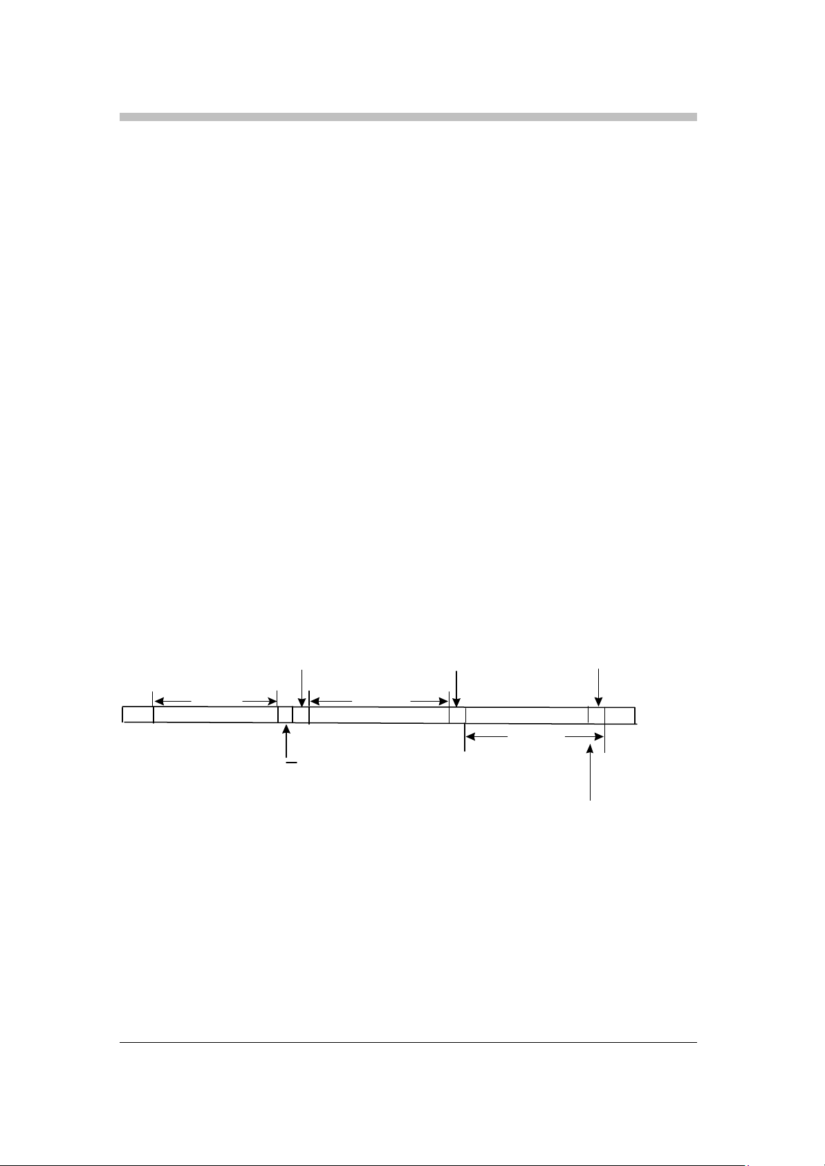
5.4.1 I2C Write to HDM8513A
The master initiates communication with the HDM8513A by generating a start condition and then
sending the HDM8513A the slave address defined by the seven bit hardwired address on HI_DATA
[6:0]. Per I2C convention, the eighth bit in the address byte is a read/not write bit, and should be
set to zero. The HDM8513A will acknowledge the correctly sent slave address, following which the
master sends an eight bit word address; this is the address of the first HDM8513A register to be
written to. Once the word address has been acknowledged by the HDM8513A, the master can
then transmit the byte to be written to the word address. Once this byte is acknowledged by the
HDM8513A, the word address is automatically incremented and further data bytes may be
transmitted by the master as necessary; one transmission may therefore contain a number of
bytes of data to be written to a sequential set of addresses (dummy bytes should be written to
addresses not defined in the HDM8513A register set to continue this process). The process is
terminated by the master generating a stop condition. Figure 25 depicts this protocol.
FIGURE 26: I2C WRITE TO THE HDM8513A
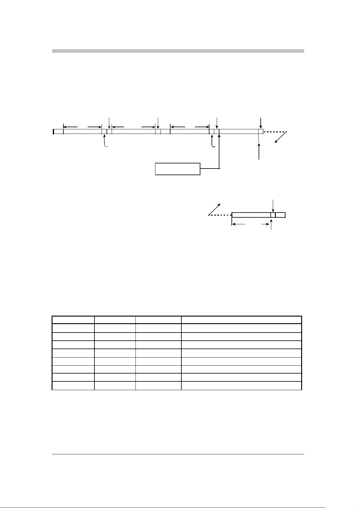
5.4.2 I2C Read from the HDM8513A
To read information from the HDM8513A, the master must first write the desired word address.
Hence the master must first generate a start condition and transmit the seven bit HDM8513A slave
address defined on HI_DATA[6:0], with the eighth bit (read/not write) set to zero. Once this has
been acknowledged by the HDM8513A, the master transmits the first word address from which it
wishes to read information. The master must then generate a second start condition and
Page 42
42
S
SLAVE ADDRESS
0AWORD ADDRESS
ASSLAVE ADDRESS
1ADATA BYTE
A
7 Bits
8 Bits
7 Bits
from slave
R/W
from slave
R/W
DATA BYTE
A
P
acknowledgement
last byte
HDM8513A becomes
retransmit the HDM8513A slave address, this time with the read/not write bit set to one (read).
This will be acknowledged by the HDM8513A, which then assumes the role of slave transmitter
and transmits the requested byte. This byte should be acknowledged by the master receiver. If no
stop condition is generated by the master, the HDM8513A will increment its word address pointer
and transmit the next byte of information. This process is detailed in Figure 26.
acknowledgement
acknowledgement
slave transmitter
acknowledgement
from slave
acknowledgement
from master
auto increment
memory word address
S: Start Condition
A: Acknowledge
P: Stop Condition
FIGURE 27: I2C R EAD FROM THE HDM8513A
Table 13: I2C Slave Address
I2C_ADD0 I2C_ADD1 I2C_ADD2 I2C Address
0 0 0 0000000
1 0 0 0000011
0 1 0 0001100
1 1 0 0001111
0 0 1 0110000
1 0 1 0110011
0 1 1 0111100
1 1 1 0111111
from master
auto increment
memory word address
Page 43

43
6. Register Definitions
6.1 Write Registers
ADDRESS (Hex)
00, 01, 02 Symbol Timing Frequency
The 20 bit straight binary number in this field establishes the symbol
timing frequency utilized within the demodulator. Bit 7 of address 00 is
the MSB and bit 4 of address 02 is the LSB. If Rs is the symbol rate
and fc is the clock frequency, the value to be stored in this 20 bit field is
the integer portion of Rs(220)/f
03 Symbol Timing Loop Gain Control
This field establishes the K1 and K2 gain values for the second order
loop filter of the symbol tracking loop. Bits 0,1 and 2 determine the
straight-through gain, and bits 4,5,6 and 7 determine the integration
path gain. The nominal value of this parameter in Hex, is expressed
below for different ranges of symbol rate to clock rate ratios:
Symbol Rate/Clock Value
0.75 - 0.40 B6
0.40 - 0.20 A5
0.20 - 0.10 94
0.10 - 0.05 83
0.05 - 0.025 72
0.025 - 0.016 61
04, 05, 06 Carrier Frequency
The 20 bit, two's complement number in this field establishes the
nominal carrier frequency of the demodulator. Bit 7 of address 04 is the
MSB and bit 4 of address 06 is the LSB. The number in this 20 bit field
multiplied by the clock frequency divided by 220 is the carrier frequency
in Hertz. When the carrier sweep function is active, this value defines
the starting frequency.
c.
Page 44

44
07, 08 Carrier Loop Filter Control
This field establishes the K1 and K2 gain values for the second order loop
filter of the carrier tracking loop. Bits 0,1,2 and 3 determine the straight through gain, and bits 4,5,6 and 7 determine the integration path gain.
The nominal value of this parameter in Hex, is expressed below for
different ranges of symbol rate to clock rate ratios. Two loop filter
configurations are provided at each symbol rate, one for steady state
operation(08) and one which is used only for acquisition(07) to permit
greater frequency pull-in. Initially the gains are set to acquisition values.
When QPSK_LOCK is achieved, they are automatically switched to
steady state values.
Symbol Rate/Clock Steady State Acqu.
0.75 - 0.40 47 77
0.40 - 0.20 47 77
0.20 - 0.10 47 77
0.10 - 0.05 46 77
0.05 - 0.025 45 77
0.025 - 0.016 45 77
09, 0A Carrier Sweep Step Size
This 16 bit value defines the size of the step of each carrier frequency
dwell. Bit 7 of address 09 is the MSB and bit 0 of address 0A is the
LSB. The number in this register is divided by 216, and multiplied by the
clock frequency to determine the frequency step increment.
0B, 0C Symbols Per Dwell
This 16 bit value defines the time, in symbol periods, for which the
demodulator wi ll dwell before making the next frequency step in a sweep.
Bit 7 of address 0B is the MSB and bit 0 of address 0C is the LSB.
0D Number of Search Frequencies
This 8 bit field determines the number of frequency steps which occur
during the frequency sweeping process. Combined with the frequency
step size, this determines the frequency span of the carrier sweep.
Page 45

45
0E Narrow Band AGC initial value
The six most significant bits of this field establish the initial gain of the
AGC. High numbers correspond to low gain associated with low symbol
rates. If the narrowband AGC function is enabled, this number is used
as a starting point and the closed loop will seek the optimum setting
without processor interaction.
Page 46

46
0F Control Parameters
Bit 0. Binary/Two’s Complement
When this bit is a zero, the system expects the six bit modulation input
samples in two’s complement format, otherwise the input should be in
offset binary format.
Bit 1. Spectrum Invert
When this bit is set to zero, the spectrum of the received signal is
inverted. This has the effect of complementing the in- phase channel
only.
Bit 2. Bias Cancel Enable
When this bit is a one, the internal circuit which cancels DC bias on the I
and Q inputs is enabled. When this function is enabled, it is assumed
that the input signal is scrambled with no significant DC component on
either the I or Q.
Bit 3. Symbol Track Enable
When this bit is set to one, the symbol tracking function is enabled.
When this bit is zero the symbol tracking frequency is forced to the
nominal 20 bit programmed value.
Bit 4. Carrier Track Enable
When this bit is set to one, the carrier phase tracking function is
enabled. When this bit is zero, the carrier frequency is forced to the 20
bit programmed value.
Bit 5. Sweep Hold
When this bit is set to one, the sweeping process is inhibited, and the
nominal carrier frequency remains at the last value.
Bit 6. Narrowband AGC Mode 1 Enable
When this bit is set to one and the narrowband AGC is in Mode 1, the
narrowband AGC self-adjusts to the optimum gain setting. When the bit
is set to zero, the most recent value is held without updating.
Bit 7. Automatic Detection of Spectrum Inversion
When this bit is set to one, the spectrum inversion is detected
automatically.
Page 47

47
10 Reset Functions
Bit 0. Symbol Timing Frequency Accumulator
When this bit is set to zero, the frequency accumulator in the symbol
tracking loop is cleared to zero. This bit must be set to one in normal
tracking operation to implement a second order tracking loop, otherwise
the loop is first order.
Bit 1. Carrier Phase Tracking Frequency Accumulator
When this bit is set to zero, the frequency accumulator in the carrier
phase tracking loop is cleared to zero. This bit must be set to one in
tracking operation to implement a second order loop filter otherwise the
loop is first order.
Bit 2. Wideband AGC Accumulator
When this bit is set to zero, the accumulator in the wideband AGC is
cleared to zero. In normal operation, this bit is set to one. When the
wideband AGC is set to Mode 1, this bit has no effect as the integrator
must be implemented in the external analog circuits.
Bit 3. Narrowband AGC Accumulator
When this bit is set to zero, the accumulator in the narrowband AGC is
cleared to the initial value defined in location 0E. In normal operation,
this bit is set to one.
Bit 4. Unused
Bit 5. Carrier Sweep Function
When this bit is set to zero, the sweep function is disabled and the
carrier frequency is forced to the preset value defined in register
locations 04, 05 and 06.
Bit 6. Viterbi Reset
When this bit is set to zero, the accumulator for the signal quality is
cleared to zero. In normal operation, this bit is set to one.
Bit 7. Reed Solomon Error Counter
When thi s bit is set to zero, the counters for the number of corrected
errors and the number of uncorrected code words are cleared to zero.
Page 48

48
11
12 LNB Tone
13 Sigma Delta
Wideband AGC Control
Bit 0. Wideband AGC Mode
When this bit is set to one (Mode 0), the WB AGC output must be
filtered with an external integrating analog filter to implement a first order
feedback loop. When this bit is zero (Mode 1), a digital integrator within
the HDM8513A performs this function and the only external analog
function required is a low pass filter t o remove the high frequency
components of the sigma delta converter output.
Bit 1. WB AGC Invert
When this bit is set to zero a high duty factor on the WB AGC output
corresponds to too much gain. When the control bit is set to one, high
duty factor corresponds to not enough gain.
Bit 2. WB AGC Hold
During normal tracking operation, this bit is set to one. When this bit is
set to zero and the wideband AGC is in Mode 1, the digital integrator is
held to the most recent value and loop updates are inhibited.
Bit 3. LNB Hold
When this bit is set to one, the output of LNB -Tone is held on zero.
Bit 4. I2C By-pass
When this bit is set to zero, SCL_I2CO and SDA_I2CO are disabled.
The default is one and Data/clock can be by-passed.
Bits [7:5]. WB AGC Gain
This three bit field defines the time constant of the WB AGC in Mode 1.
A value of zero corresponds to the shortest time constant and 7
corresponds to the slowest time constant.
This eight bit value establishes the control for LNB tone generator. If fL
is the desired frequency and fC is the clock frequency, the value to be
stored in this 8 bit field is the integer portion of fL(217)/fC. The default
value(30H) generates 22KHz tone at 60MHz sampling clock.
This eight bit input value establishes the control for Sigma Delta
converter. This function is independent of other demodulator functions
and is provided as control for external analog components.
Page 49

49
14 Test Set-up
The eight bit data written to this location defines the data presented on
the 16 bit test bus. For configurations where the data is updated once
per symbol period, the data changes at the rising edge of
SYMBOL_CLOCK
(in the case that SYMBOL_CLOCK remains high for consecutive
CLOCK
cycles, the test port data will also change accordingly during the high
period of SYMBOL_CLOCK due to the arrival of another symbol).
Bits [2:0]. Test port configuration
00H Output is tristate.
01H Test bits [15:8] provide the I baseband filter output. Test bits [7:0]
provide the Q baseband filter output. This information is updated once
per symbol period.
02H Test bits [15:0] provide the sixteen most significant bits of the
demodulator carrier phase test bits. This information is updated once
per
symbol period.
03H Test bits [15:0] provide the sixteen most significant bits of the
demodulator symbol phase test bits. This information is updated once
per
symbol period.
04H Test bits [15:8] provide the Reed Solomon output data. Test bits
[7:0] provide the deinterleaver output data. This information is updated at
the Reed Solomon clock rate; when the transport stream output is
configured to parallel output mode, DATA_CLK may be used as an
output clock for this data.
05H Test bits [15:10] provide the six bit narrowband AGC accumulator
value. Test bits [9:6] provide the four bit value of symbol phase. Test
bits [5:4] provide the two bit symbol count value. This information is
updated once per symbol period.
06H Test bits [13:8] provide the six bit I-channel data from the ADC.
Test bits [5:0] provides the six bit Q-channel data from the ADC. This
information is updated at the fixed rate sample clock.
07H In this mode the test pins are used as input pins. The internal
ADC is disabled, and the inputs at the test pins are fed directly to the
demodulator. Test bits [13:8] are used as I-channel input and test bits
[5:0] are used as Q-channel input. This information is updated at the
fixed rate sample clock.
Bit 3. Transport error Indicator Enable/Disable
Enables/Disables the transport error indicator,1 bit indicator in transport
header. When this bit is set to 1 and if transport error is internally
detected the transport error indicator bit is set to 1. When zero this
functionality is disabled.
Page 50

50
Bit 4. This bit should be fixed to zero
Bit 5. Regulated Data Clock
Enables/Disables the data and data clock regulator. When this bit is set
to 1, data output and data clock are regulated by FIFO operation. When
this bit is set to 0, internal data output and internal data clock are bypassed
Bit 6. Serial Valid
When this bit is set to 1, DATA_STB signal sustains high when valid bit
is out (mode 2). When this bit is set to 0, DATA_STB signal alternates
when every valid bit is out (mode 1). Refer to figure 12 and figure 13.
Bit 7. Clock Polarity
This bit is used to select the DATA_CLK polarity either for serial or
parallel transport interface. If this bit is set to zero(default value), the
transport data and control signals are latched at the positive edge of
DATA_CLK. Otherwise, the signals are latched at the negative edge of
DATA_CLK.
15 Viterbi Lock Threshold
Register 15 to 17 contain control parameters for synchronization in
Viterbi decoder. Ordinary users are recommended to use the default
value.
Bit[7:4] defines the lock threshold for VB_NODESYNC. Viterbi decoder
decides that the correct code rate has been found. A large number
means it takes longer to find the correct code rate in automatic
detection mode. It should be greater than 7. The default value is 12.
Bit[3:0] defines the lock fail threshold. Viterbi decoder rejects a code
rate and moves on to the next code rate. A small number means Viterbi
decoder tries more data before it moves to the next code rate. It should
be less than 7. The default value is 2.
16 Viterbi Unlock Threshold
This number defines the threshold to maintain the Viterbi lock state. A
large number means it needs more bad data to get out of the viterbi lock
state and re- start searching the correct code rate. The default value is
1.
Page 51

51
17 Viterbi Byte-Sync control
Once the viterbi lock(VB_NODESYNC) is achieved, the Viterbi decoder
tries to find the byte-sync. This 8-bit register is used to set “unlockthreshold” for the byte-sync. Large number means it needs more baddata to get out of the byte-sync state, i.e. less sensitive to noise. The
default value is 1.
Page 52

52
18 Control Parameters for Viterbi and RS Decoders
Bit 0. Parallel or Serial Output
Controls the transport stream output of the 8513A to serial or parallel
mode.
“0” (default) means the 8513A MPEG output is parallel.
“1” means the 8513A MPEG output is serial. The LSB of the data
bus(data[0] - pin 98) is used as the serial output pin.
Bit 1. MPEG2 Data
“0” (default) means the incoming data is MPEG2 decoded. In this mode
a sync byte is expected every 188 bytes.
“1” means non -MPEG2 data. The Viterbi decoder doesn’t check the
existence of the sync byte.
Bit [4:2]. Depuncturing Rate
It defines the depuncturing rate of the Viterbi decoder. When
vb_autocode is disabled, the depuncturing rate is set to this value.
0 --- 1/2
1 --- 2/3
2 --- 3/4
3 --- 5/6
4 --- 7/8
5 --- 6/7
Bit 5. Viterbi Auto Decoding Mode
When this bit is set to 1, the Viterbi decoder automatically finds the
correct code rate of the incoming signal. When this bit is set to 0, the
code rate is set to the user-defined value at bit[4:2]. The default is 0.
Bit 6. DSS Mode
When this bit is set to 0, this device operates as DVB mode. When
this bit is set to 1, this device operates as DSS mode. In that case, the
roll-off factor of the Nyquist filter is set to 0.2. The default is 0 (DVB).
Bit 7. BPSK Mode
When this bit is set to 0, the demodulator assumes the incoming data
is QPSK-modulated. When this bit is set to 1, the demodulator
assumes the incoming data is BPSK -modulated.
19 Rate 1/2 Threshold Select
This seven bit parameter defines the threshold used in the Viterbi
decoder node synchronization process. For rate 1/2, the nominal value
is 30 (1EH).
Page 53

53
1A Rate 2/3 Threshold Select
This seven bit parameter defines the threshold used in the node
synchronization process. For rate 2/3, the nominal value is 30 (1EH).
1B Rate 3/4 Threshold Select
This seven bit parameter defines the threshold used in the node
synchronization process. For rate 3/4, the nominal value is 40 (28H).
1C Rate 5/6 Threshold Select
This seven bit parameter defines the threshold used in the node
synchronization process. For rate 5/6, the nominal value is 60 (3CH).
1D Rate 6/7 Threshold Select
This seven bit parameter defines the threshold used in the node
synchronization process. For rate 6/7, the nominal value is 60 (3CH).
1E Rate 7/8 Threshold Select
This seven bit parameter defines the threshold used in the node
synchronization process. For rate 7/8, the nominal value is 60 (3CH).
Bit 7. This bit should be fixed to zero.
Page 54

54
1F Clock Generation PLL Control
An integrated VCO is locked to MxN times a reference frequency
provided by a external clock
Bits [4:0]. N Divider ratio
It defi nes a feedback divider with a divider ratio N. The dafault is 15
(0FH).
Bit 5. M Divider ratio
It defines a reference divider with a divider ratio M. When this bit is set
to 1, the divider ratio M is 4. When this bit is set to 0, the divider ratio M
is 1. The default is 1.
Bit 6. PLL Enable
When this bit is set to 1, the generated clock of the PLL is connected
to the internal clock. When this bit is set to 0, the PLL is bypassed
and the external clock signal is directly connected to the internal
clock. The default is 0.
Bit 7. This bit should be fixed to zero.
Page 55

55
fint_clk
fext_clk
fint_clk
=
fext_clk
Example for determination of internal clock
Desired internal clock:
N divider ratio range: 1 – 31 (integer)
M divider ratio range: 1 or 4 (integer)
Calculation is as follows:
<Example 1>
Desired internal clock: 60MHz
External clock supplied: 16MHz
N divider ratio range: 1 – 31 (integer)
M divider ratio range: 1 or 4 (integer)
Calculation is as follows: 60 =16 x N/M
Case M =4, N must be 15
Case M =1, N is impossible
Only one possible case exists
<Example 2>
Desired internal clock: 60MHz
External clock supplied: 4MHz
N divider ratio range: 1 – 31 (integer)
M divider ratio range: 1 or 4 (integer)
Calculation is as follows: 60 =4 x N/M
Case M =1, N must be 15
Case M =4, N is impossible
Only one possible case exists.
Externa l clock supplied:
N
M
Page 56

56
6.2 Read Registers
ADDRESS (Hex)
00
01, 02, 03 Symbol Timing Frequency Accumulator
04, 05, 06 Phase Tracking Frequency Accumulator
07 QPSK Lock Status
08
09, 0A
Narrowband AGC Accumulator
The current value of the si x bit AGC accumulator may be read from this
location.
The current value of the 20 frequency accumulator in the symbol timing
loop filter may be read from these 3 locations. Bit 7 of address 01 is the
MSB and bit 4 of address 03 is the LSB.
The current value of the 20 bit frequency accumulator in the carrier phase
loop filter may be read from these 3 locations. Bit 7 of address 04 is the
MSB and bit 4 of address 06 is the LSB.
Bit 0. QPSK Lock Flag
When this bit is set to one, the QPSK demodulator is phase locked.
Wide Band AGC Accumulator
This eight bit value represents the most significant bits of the accumulator
in the first order wideband AGC loop. This data only has meaning when
the wideband AGC is in Mode 0.
Sweep Frequency
The 16 bit sweep accumulator is available at this location. Bit 7 of address
09 is the MSB and bit 0 of address 0A is the LSB. The receiver frequency
is determined by adding the Sweep Frequency with the carrier frequency
accumulator (read addresses 04, 05 and 06) and the nominal carrier start
frequency (write addresses 04, 05 and 06).
Page 57

57
0B In-Phase
The eight bit output of the In-phase baseband filter is available at this
location. This data is updated once per symbol.
0C Quadrature
The eight bit output of the quadrature baseband filter is available at this
location. This data is updated once per symbol.
0D Noise Power
This eight bit output provides a measure of the noise component of the
signal when QPSK lock is achieved. Higher numbers correspond to lower
signal-to- noise ratio conditions. The quality of this metric is improved if
the narrowband AGC is disabled for a minimum of 1000 symbol periods
before this parameter is read.
0E, 0F
16,17,18 Signal Quality
19 Viterbi Rate
1A Reed Solomon Errors
BER Calculator
The current value of the 16bit BER is used to monitor the signal quality or
estimate the SNR of incoming signal at the output of Viterbi. Bit 7 of
address 0E is the MSB and bit 0 of address 0F is the LSB. It represents
the number of errors among 220 data bits.
This 24 bit signal provides a measure of quality of the signal processed by
the Viterbi decoder. This parameter can be used to infer bit error rate and
input signal-to- noise ratio for signals which are within a few dB of threshold.
Bit 7 of address 16 is the MSB and bit 0 of address 18 is the LSB.
The specific definition of this signal for each coding rate is TBD.
This three bit number represents the code rate of the Viterbi decoder.
Rate 1/2 0
Rate 2/3 1
Rate 3/4 2
Rate 5/6 3
Rate 7/8 4
The four bit number at this location indicates the number of errors
corrected in the most current block of 188 bytes. This number may range
from 0 to 8.
Page 58

58
1B
1C,1D Accumulated Reed Solomon Errors
1E Acc umulated Reed Solomon Data
1F Device Identifier
FEC Lock
Bit 0. Viterbi Node Sync
When this bit is set to one, the Viterbi decoder has successfully
established node synchronization.
Bit 1. Frame Sync
When this bit is set to one, the FEC chip has successfully established
word sync and frame sync.
Bit 2. Viterbi Byte Sync
When this bit is set to one, the Viterbi decoder has successfully
established byte-synchronization.
Bit 3. Pi Ambiguity
When this bit is set to one, the Viterbi decoder has successfully
resolved pi ambiguity in the input data. (i.e inverted data)
Bit 4. Pi/2 Ambiguity
When this bit is set to one, the Viterbi decoder has successfully
resolved pi/2 ambiguity in the input data
These two registers present a count of corrected errors since it was last
reset. Bit 7 of address 1C is the MSB and bit 0 of address 1D is the
LSB. These registers are reset by writing value to address 10H.
This register presents a count of the uncorrected code words since it
was last reset. When it reaches its maximum count(255), it rolls back
to zero
and starts counting again. This register is reset by writing value to
address 10H.
This register present device identifier. The current value of this register
is
93H
Page 59

59
Appendix
Page 60
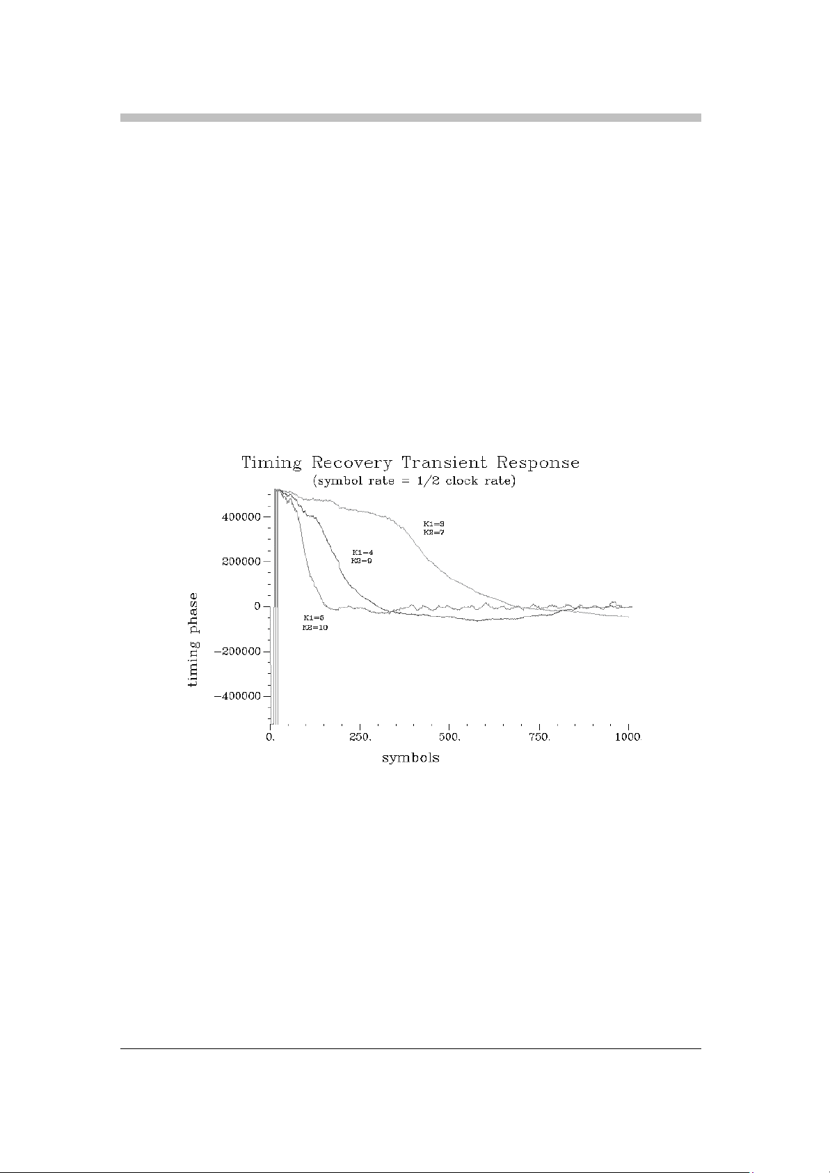
60
A1. Loop Filter Programming A pplication Note
To illustrate that the symbol timing recovery loop and the carrier phase recovery loop are both
programmable, several simulations were performed with different loop parameter conditions. These
simulations were performed with a symbol rat e of two samples per symbol, corresponding to 30M
symbols-per-second if a 60MHz clock were utilized.
Figure A1 illustrates the transient response of the symbol phase with three different loop conditions
(K1=5, K2=10; K1=4, K2=9; and K1=8, K2=7). The vertical scale represents phase over a 360
degree range (524,287 to -524,288). All test cases were run at high signal-to-noise ratio. The
highest gain condition could be used for fast acquisition as well as for steady state with high code
rate conditions, while the intermediate gain is a suitable steady state setting for rate 1/2 codes
(minimum Eb/N0 of 4 dB). The lowest gain setting corresponds to ultra low loop bandwidth and
may be considered for maintaining lock without phase jumps during deep signal fades.
FIGURE A1: SYMBOL TIMING RECOVERY TRANSIENT RESPONSE
Page 61
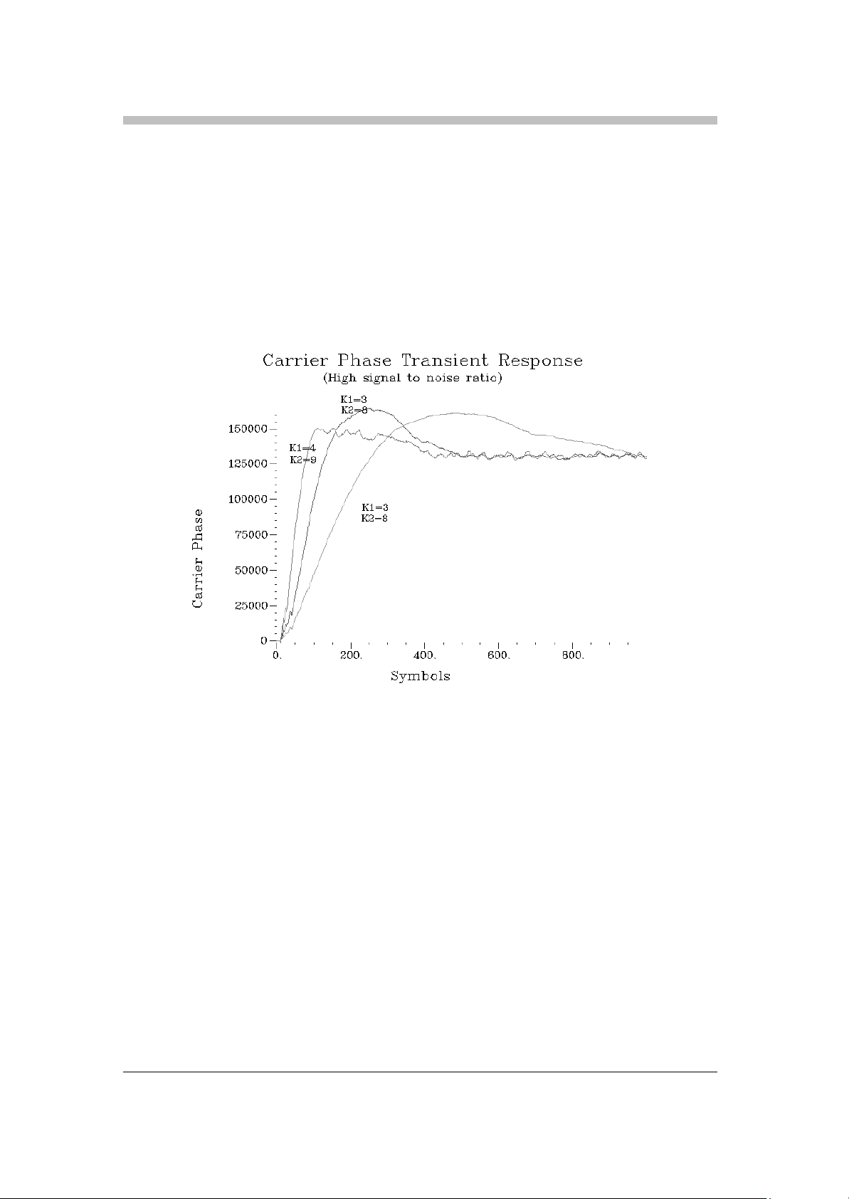
61
Figure A2 illustrates the transient response of the carrier tracking loop with the same loop
bandwidth settings at high signal-to-noise ratio. The phase step for this test corresponds to 45
degrees. The actual bandwidth of the carrier loop is greater than that of the symbol loop for the
same settings because the carrier loop must cope with greater dynamics (such as frequency offset
and drift). Figure A3 illustrates the transient response of the carrier phase tracking loop under the
same conditions at minimum signal- to-noise ratio (Eb/N0 of 4 dB with rate 1/2 coding). The
highest bandwidth case will pull in with a carrier frequency error of + or - .005 of the symbol rate at
this minimum signal level. Higher loop bandwidth may be programmed to provide greater pull -in
with higher signal-to-noise ratio conditions.
FIGURE A2: CARRIER P HASE RECOVERY TRANSIENT RESPONSE
Page 62
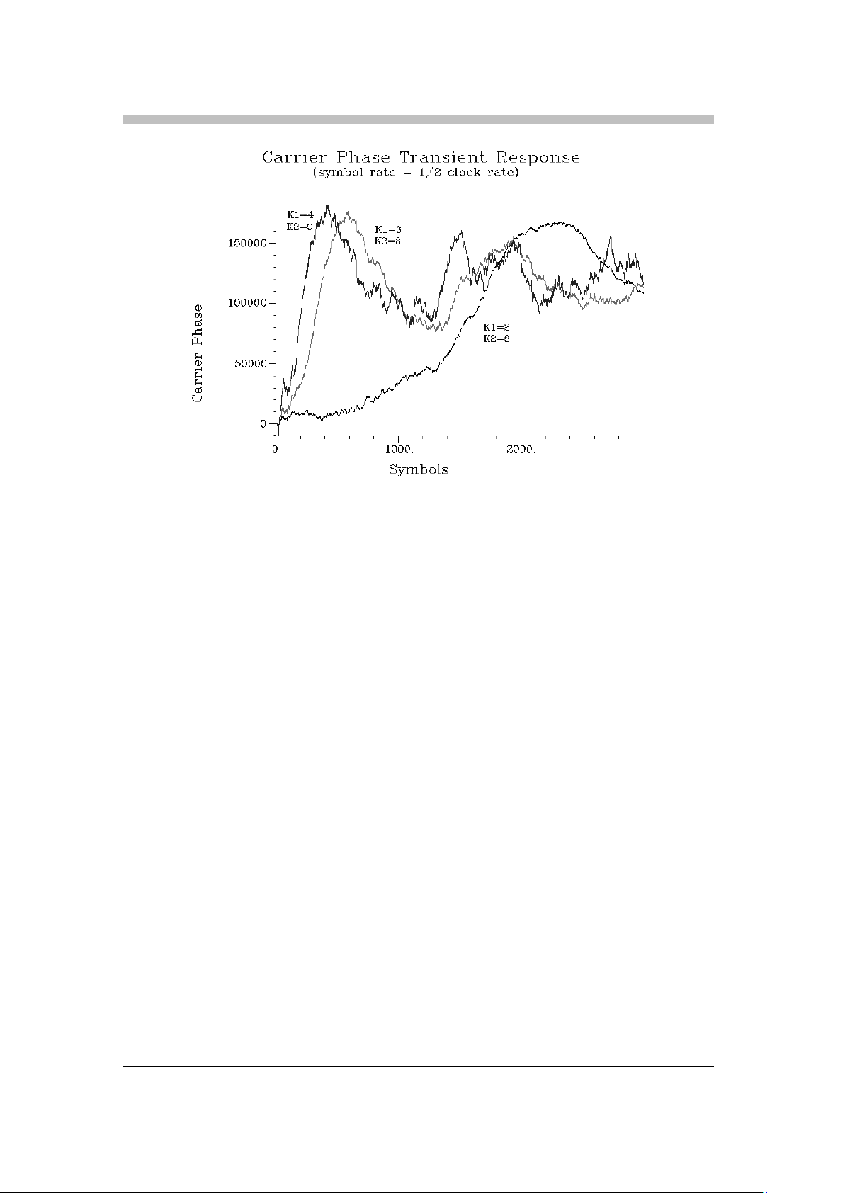
62
FIGURE A3: CARRIER PHASE RECOVERY TRANSIENT RESPONSE WITH LOW SNR
Page 63

63
A2. False Lock Escape Application Note
A QPSK signal will have inherent false lock states at frequency offsets of + or - n/4 of the symbol
rate. Most DBS signals which have symbol rates of 20M symbols-per -second or higher will not
experience false lock because the carrier frequency uncertainty is less than 1/4 of the symbol rate.
The HDM8513A is designed to process low data rate signals which may experience false lock,
particularly at high signal- to-noise ratio conditions. The HDM8513A will permit recovery from false
lock with some added host processor interaction. Specifically, the processor must initialize the
internal carrier frequency search hardware to search over a carrier frequency range of 1/4 of the
symbol rate. If QPSK lock is achieved, but no Viterbi lock is achieved, the processor would
assume this is a false carrier lock, then program the HDM8513A to search another carrier
frequency range covering 1/4 of the symbol rate. When both QPSK lock and Viterbi lock have
been achieved, the search is completed. This technique is reliable because the HDM8513A
utilizes a fixed frequency clock which is not subject to inaccuracy associated with analog VCOs.
This accuracy insures that the multiple search ranges are perfectly continuous with respect to
each other with no overlap.
Page 64

64
A3. Performance with Interference.
In order to evaluate the filter employed within the HDM8513A with respect to attenuating out -ofband interference, a tes t was performed utilizing the COSSAP simulator. The desired signal, at
zero frequency, was configured to utilize 16 samples -per-symbol (corresponding to 3.75MHz
symbol rate if a 60MHz clock is employed). An interfering signal was added with the same
characteristics, except that the amplitude was made to be 10dB higher than that of the desired
signal, the data pattern was different and the carrier frequency was offset from that of the desired
signal. Several offset frequencies were evaluated for this cas e. Figure A4 illustrates the spectrum
of the test condition when the offset frequency is 1.35 times the symbol rate.
Figure A5 illustrates the measured bit error rate for various conditions. The error rate on the I
channel was measured separately from that of the Q channel, and the horizontal axis is scaled in
dB for one component (I or Q of the signal). For example, the point labeled 1dB corresponds to
SNR (noise bandwidth = symbol rate) of 4dB or Eb/N0 of 4dB if rate 1/2 coding is employed.
The theoretical performance for coherent PSK is shown with the solid line. The curve closest to
theoretical is the demodulator performance with no other interferers and corresponds to an
implementation loss of about 0.2dB. When the interferer was placed at a frequency of either 2.0 or
1.35 times the symbol rate away from the desired carrier, there is an additional degradation ranging
from 0dB to 0.1dB. The worst case occurs when the interferer is placed at only 1.28 times the
symbol rate from the carrier of the desired signal. In this case, the performance has degraded with
respect to the no interference case by 0.3 to 0.5dB.
Figure A6 illustrates performance with an interferer which is 20dB higher than the desired signal
and separated in frequency by 2 times the symbol rate. In this case, the performance has
degraded by 0.7 to 0.8dB from the case with no interferer.
Page 65
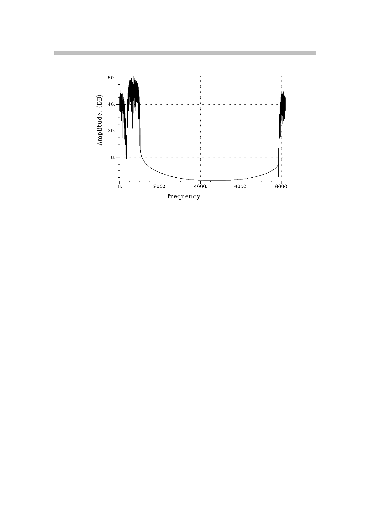
65
FIGURE A4: ADJACENT CHANNEL INTERFERENCE OF 10 DB, 1.35 S PACING
Page 66
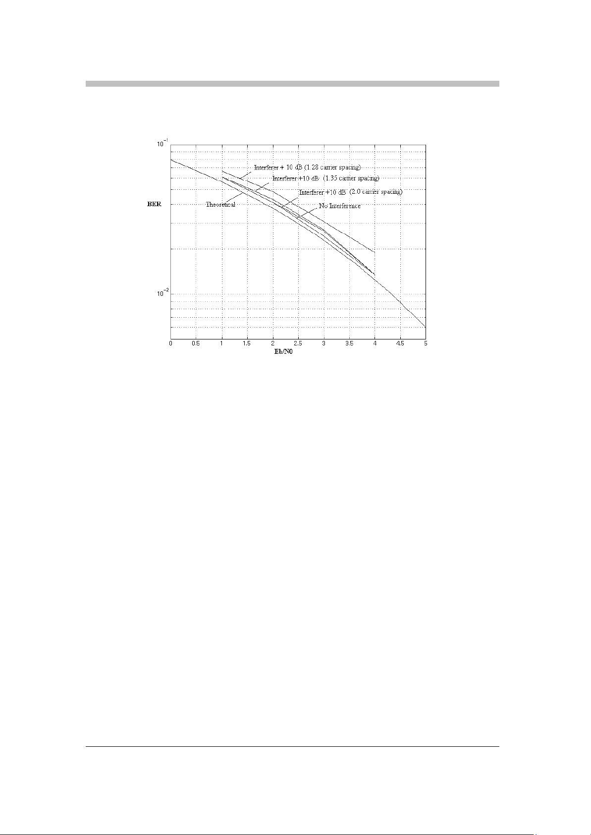
66
FIGURE A5: PERFORMANCE WITH INTERFERER AT DIFFERENT CARRIER SPACINGS
Page 67
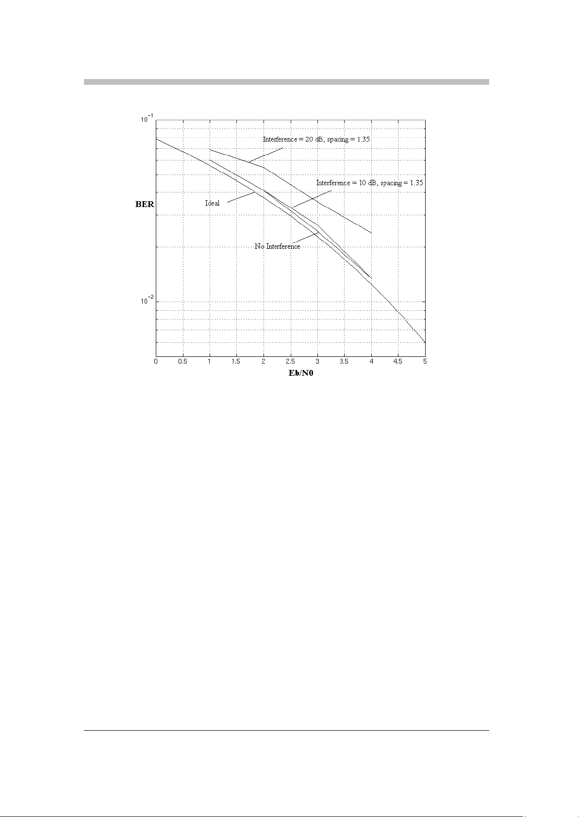
67
FIGURE A6: PERFORMANCE WITH +10 DB I NTERFERER
Page 68

68
A4. Nyquist Criteria Considerations
The HDM8513A is clocked at 60MHz, yet processes signals with symbol rates as high as 45M
symbols-per-second. At fir st thought, this might appear to be violating the Nyquist criteria which
states that the sampling rate must be at least twice the highest frequency component. The total
bandwidth of the 45Msps signal, with 35% excess bandwidth, is about 60MHz.
The samples provided to the HDM8513A are complex samples, which is equivalent to 120M
samples-per-second, which does satisfy the Nyquist criteria. Another way of looking at this is to
examine the baseband signal. The signal bandwidth covers 60MHz, but the baseband spectrum
covers from -30MHz to +30MHz. There are no baseband frequency components greater than
30MHz, and the 60MHz clock is adequate as long as complex samples are taken.
 Loading...