

Page 1

HD74HC93
4-bit Binary Counter
Description
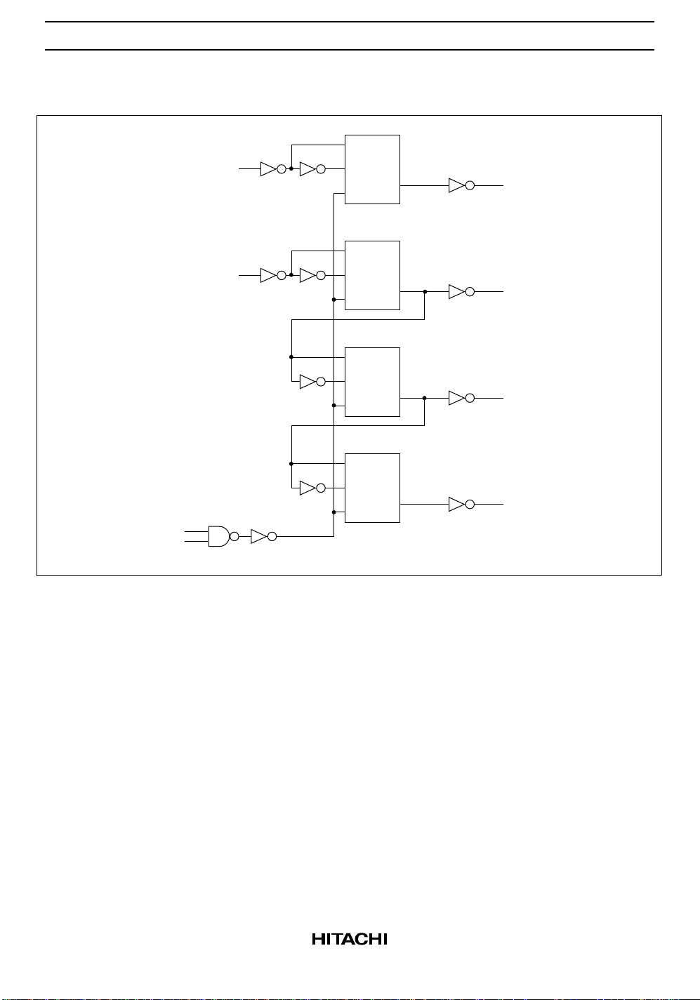
The HD74HC93 is a 4-bit ripple type counter consisting of four master/slave flip-flops that are internally
connected to provide separate divide-by-two and divide-by-eight sections. Each section has a separate
clock input which initiates state changes of the counter on the high-to-low clock transition. State changes
of the Q outputs do not occur simultaneously because of internal ripple delays. Therefore, decoded output
signals are subject to decoding spikes and should not be used as clocks or as strobes except when gated
with the clock of the HD74HC93. QA is the output of the divide-by-two section; QB, QC, and QD are the
binary outputs of the divide-by-eight section.
A gated AND asynchronous reset is provided which resets all the flip-flops.
Because the output from the divide-by-two section is not internally connected to the succeeding stages, the
devices may be operated in various counting modes:
1. A 4-bit rippl counter – The QA output must be externally connected to the clock B input. The input
count pulses are applied to the clock A inputl. Simultaneous divisions of 2, 4, 8 and 16 are performed at
the QA, QB, QC and QD outputs.
2. A 3-bit ripple counter – The input count pulses are applied to the clock B input. Simultaneous
frequency divisions of 2, 4 and 8 are available at the QB, QC and QD outputs. Independent use of the
first flip-flop is available if the reset function coincides with reset of the 3-bit ripple-through counter.
Features
• High Speed Operation: tpd (A to QA) = 13 ns typ (CL = 50 pF)
• High Output Current: Fanout of 10 LSTTL Loads
• Wide Operating Voltage: VCC = 2 to 6 V
• Low Input Current: 1 µA max
• Low Quiescent Supply Current: ICC (static) = 4 µA max (Ta = 25°C)
Page 2
HD74HC93
Function Table
Reset/Count Function Table
Reset Inputs Outputs
R
0(1)
R
0(2)
HHLLLL
L×Count
× L Count
BCD Count Sequence
Outputs
Count Q
0L L L L
1L L L H
2L L H L
3L L H H
4L H L L
5L H L H
6L H H L
7L H H H
8H L L L
9H L L H
10HL HL
11HL HH
12 H H L L
13 H H L H
14HHHL
15HHHH
Notes: Output QA is connected to input B for BCD count.
D
Q
D
Q
C
Q
C
Q
B
Q
B
Q
A
Q
A
2
Page 3
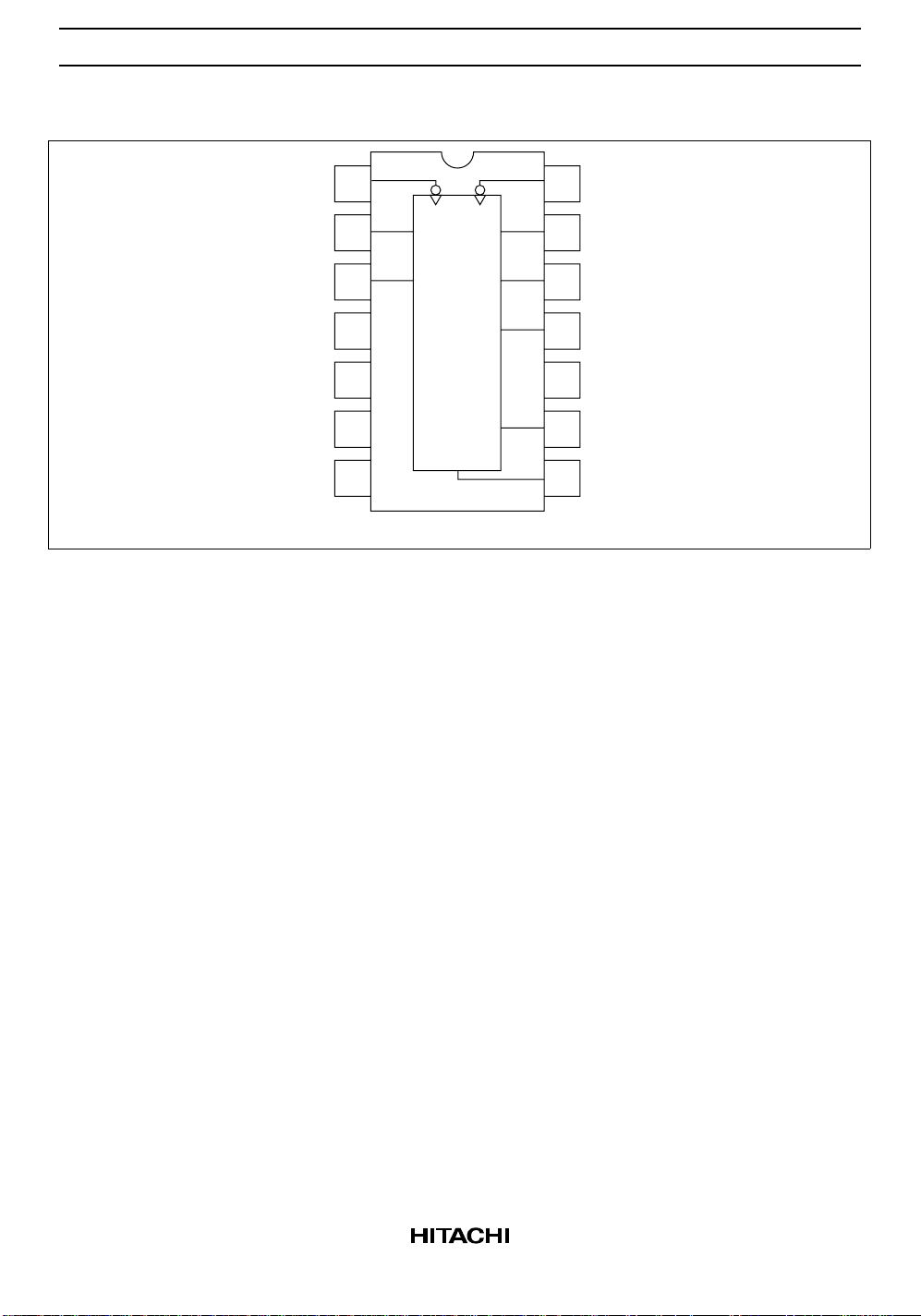
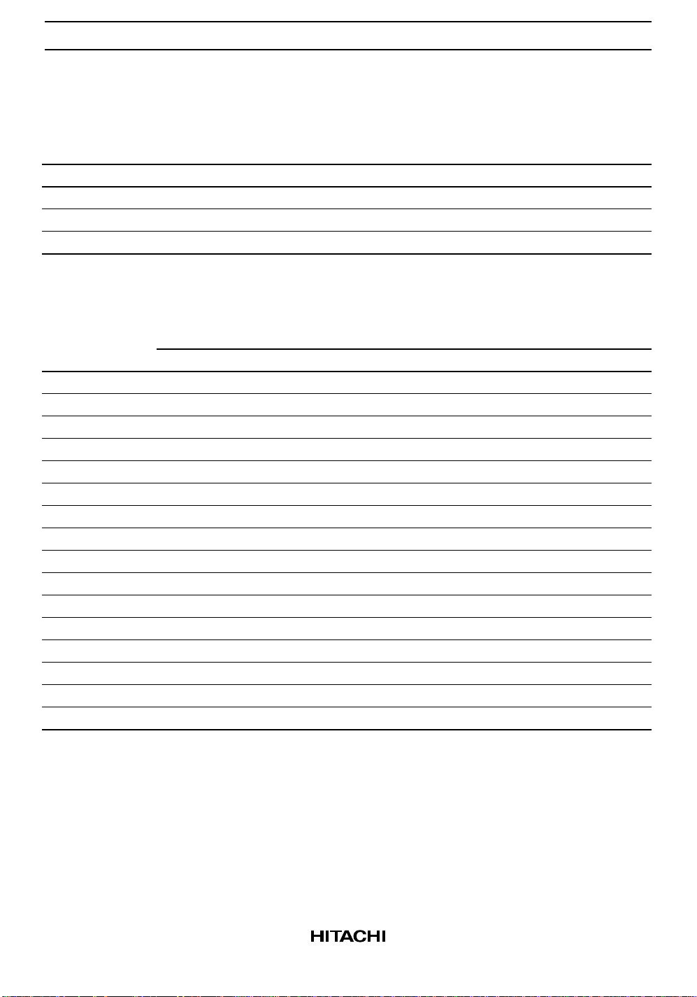
Pin Arrangement
HD74HC93
B
0(1)
R
R0(2)
NC
Vcc
NC
NC
1
2
3
4
5
6
7
BA
R0(1)
QA
R0(2)
QD
QB
C
Q
(Top View)
14
13
12
11
10
A
NC
A
Q
QD
GND
B
Q
9
QC
8
3
Page 4
HD74HC93
Block Diagram
Input A
Input B
C
Q
C
A
Q
R
C
Q
C
Q
R
C
Q
C
Q
R
Q
B
Q
C
Q
R0(1)
R0(2)
C
Q
C
D
Q
R
Q
4
Page 5

HD74HC93
DC Characteristics
Ta = –40 to
Ta = 25°C
Item Symbol V
Input voltage V
IH
(V) Min Typ Max Min Max Unit Test Conditions
CC
2.0 1.5 — — 1.5 — V
4.5 3.15 — — 3.15 —
6.0 4.2 — — 4.2 —
V
IL
2.0 — — 0.5 — 0.5 V
4.5 — — 1.35 — 1.35
6.0 — — 1.8 — 1.8
Output voltage V
OH
2.0 1.9 2.0 — 1.9 — V Vin = VIH or VILIOH = –20 µA
4.5 4.4 4.5 — 4.4 —
6.0 5.9 6.0 — 5.9 —
4.5 4.18 — — 4.13 — IOH = –4 mA
6.0 5.68 — — 5.63 — IOH = –5.2 mA
V
OL
2.0 — 0.0 0.1 — 0.1 V Vin = VIH or VILIOL = 20 µA
4.5 — 0.0 0.1 — 0.1
6.0 — 0.0 0.1 — 0.1
4.5 — — 0.26 — 0.33 IOL = 4 mA
6.0 — — 0.26 — 0.33 IOL = 5.2 mA
Input current Iin 6.0 — — ±0.1 — ±1.0 µA Vin = VCC or GND
Quiescent supply
I
CC
6.0 — — 4.0 — 40 µA Vin = VCC or GND, Iout = 0 µA
current
+85°C
5
Page 6

HD74HC93
AC Characteristics (CL = 50 pF, Input tr = tf = 6 ns)
Ta = –40 to
Ta = 25°C
Item Symbol V
Maximum clock f
max
(V) Min Typ Max Min Max Unit Test Conditions
CC
2.0 — — 5 — 4 MHz
frequency 4.5 — — 27 — 21
6.0 — — 32 — 25
Propagation delay t
time t
PLH
PHL
2.0 — — 120 — 150 ns A to Q
4.5 — 13 24 — 30
6.0 — — 20 — 26
t
PLH
t
PHL
2.0 — — 340 — 425 ns A to Q
4.5 — 42 68 — 85
6.0 — — 58 — 72
t
PLH
t
PHL
2.0 — — 130 — 165 ns B to Q
4.5 — 13 26 — 33
6.0 — — 22 — 28
t
PLH
t
PHL
2.0 — — 185 — 230 ns B to Q
4.5 — 21 37 — 46
6.0 — — 31 — 39
t
PLH
t
PHL
2.0 — — 220 — 275 ns B to Q
4.5 — 27 44 — 55
6.0 — — 37 — 47
t
PLH
t
PHL
2.0 — — 175 — 220 ns Set-to-0 to Q
4.5 — 13 35 — 44
6.0 — — 30 — 37
Output rise/fall t
time t
TLH
THL
2.0 — — 75 — 95 ns
4.5 — 5 15 — 19
6.0 — — 13 — 16
Input capacitance Cin — — 5 10 — 10 pF
+85°C
A
D
B
C
D
A to D
6
Page 7

1
19.20
20.32 Max
1.30
Unit: mm
814
6.30
7.40 Max
7
2.54 ± 0.25
2.39 Max
0.48 ± 0.10
2.54 Min 5.06 Max
0.51 Min
Hitachi Code
JEDEC
EIAJ
Weight
7.62
+ 0.10
0.25
– 0.05
0° – 15°
(reference value)
DP-14
Conforms
Conforms
0.97 g
Page 8

14
1.27
10.5 Max
1
10.06
1.42 Max
Unit: mm
8
5.5
7
+ 0.20
7.80
– 0.30
2.20 Max
*0.22 ± 0.05
1.15
0.20 ± 0.04
0° – 8°
0.70 ± 0.20
*0.42 ± 0.08
0.40 ± 0.06
*Dimension including the plating thickness
Base material dimension
0.12
0.10 ± 0.10
0.15
M
Hitachi Code
JEDEC
EIAJ
(reference value)
Weight
FP-14DA
—
Conforms
0.23 g
Page 9

9.05 Max
14
Unit: mm
8.65
8
*Pd plating
1
0.635 Max
1.27
*0.40 ± 0.06
7
+ 0.11
0.25
3.95
– 0.04
0.14
0.15
1.75 Max
M
6.10
1.08
*0.20 ± 0.05
+ 0.67
0.60
– 0.20
Hitachi Code
JEDEC
EIAJ
Weight
+ 0.10
– 0.30
0° – 8°
(reference value)
FP-14DN
Conforms
Conforms
0.13 g
Page 10

14 8
17
+0.08
*0.22
–0.07
0.20 ± 0.06
5.00
5.30 Max
0.83 Max
0.65
0.13
Unit: mm
4.40
1.0
M
6.40 ± 0.20
0.10
1.10 Max
*Dimension including the plating thickness
Base material dimension
0.15 ± 0.04
*0.17 ± 0.05
+0.03
–0.04
0.07
0° – 8°
Hitachi Code
JEDEC
EIAJ
(reference value)
Weight
0.50 ± 0.10
TTP-14D
—
—
0.05 g
Page 11

Cautions
1. Hitachi neither warrants nor grants licenses of any rights of Hitachi’s or any third party’s patent,
copyright, trademark, or other intellectual property rights for information contained in this document.
Hitachi bears no responsibility for problems that may arise with third party’s rights, including
intellectual property rights, in connection with use of the information contained in this document.
2. Products and product specifications may be subject to change without notice. Confirm that you have
received the latest product standards or specifications before final design, purchase or use.
3. Hitachi makes every attempt to ensure that its products are of high quality and reliability. However,
contact Hitachi’s sales office before using the product in an application that demands especially high
quality and reliability or where its failure or malfunction may directly threaten human life or cause risk
of bodily injury, such as aerospace, aeronautics, nuclear power, combustion control, transportation,
traffic, safety equipment or medical equipment for life support.
4. Design your application so that the product is used within the ranges guaranteed by Hitachi particularly
for maximum rating, operating supply voltage range, heat radiation characteristics, installation
conditions and other characteristics. Hitachi bears no responsibility for failure or damage when used
beyond the guaranteed ranges. Even within the guaranteed ranges, consider normally foreseeable
failure rates or failure modes in semiconductor devices and employ systemic measures such as failsafes, so that the equipment incorporating Hitachi product does not cause bodily injury, fire or other
consequential damage due to operation of the Hitachi product.
5. This product is not designed to be radiation resistant.
6. No one is permitted to reproduce or duplicate, in any form, the whole or part of this document without
written approval from Hitachi.
7. Contact Hitachi’s sales office for any questions regarding this document or Hitachi semiconductor
products.
Hitachi, Ltd.
Semiconductor & Integrated Circuits.
Nippon Bldg., 2-6-2, Ohte-machi, Chiyoda-ku, Tokyo 100-0004, Japan
Tel: Tokyo (03) 3270-2111 Fax: (03) 3270-5109
URL NorthAmerica : http:semiconductor.hitachi.com/
For further information write to:
Hitachi Semiconductor
(America) Inc.
179 East Tasman Drive,
San Jose,CA 95134
Tel: <1> (408) 433-1990
Fax: <1>(408) 433-0223
Europe : http://www.hitachi-eu.com/hel/ecg
Asia (Singapore) : http://www.has.hitachi.com.sg/grp3/sicd/index.htm
Asia (Taiwan) : http://www.hitachi.com.tw/E/Product/SICD_Frame.htm
Asia (HongKong) : http://www.hitachi.com.hk/eng/bo/grp3/index.htm
Japan : http://www.hitachi.co.jp/Sicd/indx.htm
Hitachi Europe GmbH
Electronic components Group
Dornacher Stra§e 3
D-85622 Feldkirchen, Munich
Germany
Tel: <49> (89) 9 9180-0
Fax: <49> (89) 9 29 30 00
Hitachi Europe Ltd.
Electronic Components Group.
Whitebrook Park
Lower Cookham Road
Maidenhead
Berkshire SL6 8YA, United Kingdom
Tel: <44> (1628) 585000
Fax: <44> (1628) 778322
Hitachi Asia Pte. Ltd.
16 Collyer Quay #20-00
Hitachi Tower
Singapore 049318
Tel: 535-2100
Fax: 535-1533
Hitachi Asia Ltd.
Taipei Branch Office
3F, Hung Kuo Building. No.167,
Tun-Hwa North Road, Taipei (105)
Tel: <886> (2) 2718-3666
Fax: <886> (2) 2718-8180
Copyright ' Hitachi, Ltd., 1999. All rights reserved. Printed in Japan.
Hitachi Asia (Hong Kong) Ltd.
Group III (Electronic Components)
7/F., North Tower, World Finance Centre,
Harbour City, Canton Road, Tsim Sha Tsui,
Kowloon, Hong Kong
Tel: <852> (2) 735 9218
Fax: <852> (2) 730 0281
Telex: 40815 HITEC HX
 Loading...