

Page 1
HD74HC4538
Dual Precision Retriggerable/Resettable Monostable
Multivibrators
Description
Each multivibrator features both a negative, A, and a positive, B, transition triggered input, either of which
can be used as an inhibit input. Also included is a clear input that when taken low resets the one short. The
HD74HC4538 is retriggerable. That is, it may be triggered repeatedly while their outputs are generating a
pulse and the pulse will be extended.
Pulse width stability over a wide range of temperature. The output pulse equation is simply: tw = 0.7 (R)
(C).
Features
• High Speed Operation: tpd (A or B to Y) = 22 ns typ (CL = 50 pF)
• High Output Current: Fanout of 10 LSTTL Loads
• Wide Operating Voltage: VCC = 2 to 6 V
• Low Input Current: 1 µA max
• Low Quiescent Supply Current
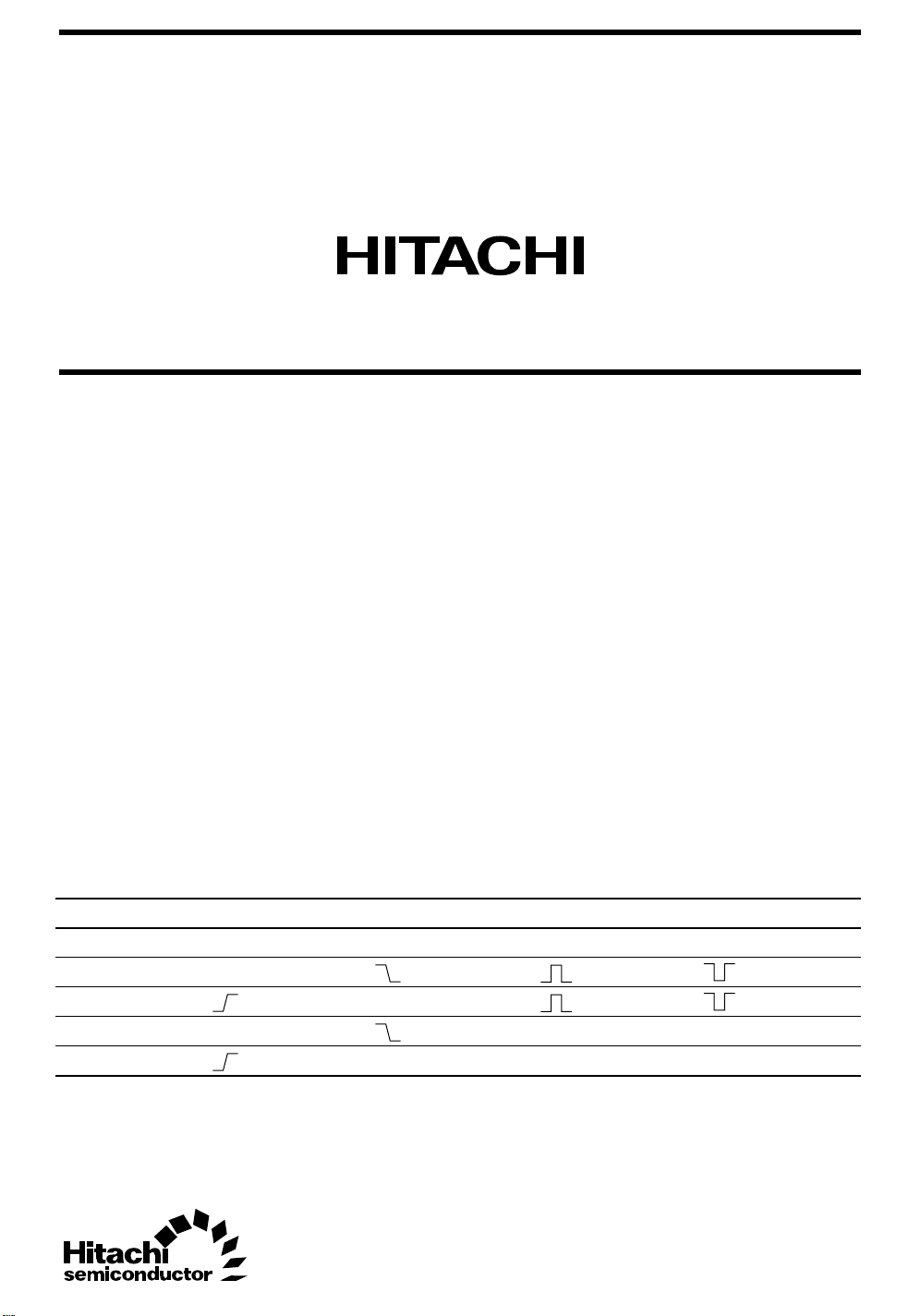
Function Table
Inputs Outputs
C
D
LXXLH
HL
H H
HH Not triggered
H L Not triggered
X : Irrelevant
ABQQ
Page 2
HD74HC4538
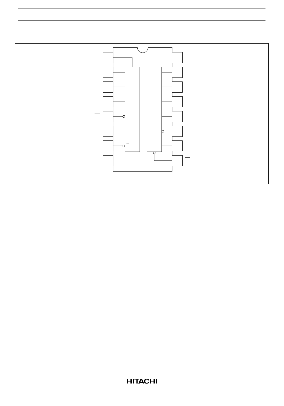
Pin Arrangement
T
1A
T
2A
CD
A
B
Q
Q
GND
1
T
2
3
A
4
A
5
A
6
A
7
A
T
CD
A
B
Q
Q
1
2
T
T
CD
Q
8
16
V
CC
15
14
13
12
11
10
T
1B
T
2B
CD
B
A
B
B
B
Q
B
9
Q
B
1
2
A
B
Q
(Top view)
2
Page 3

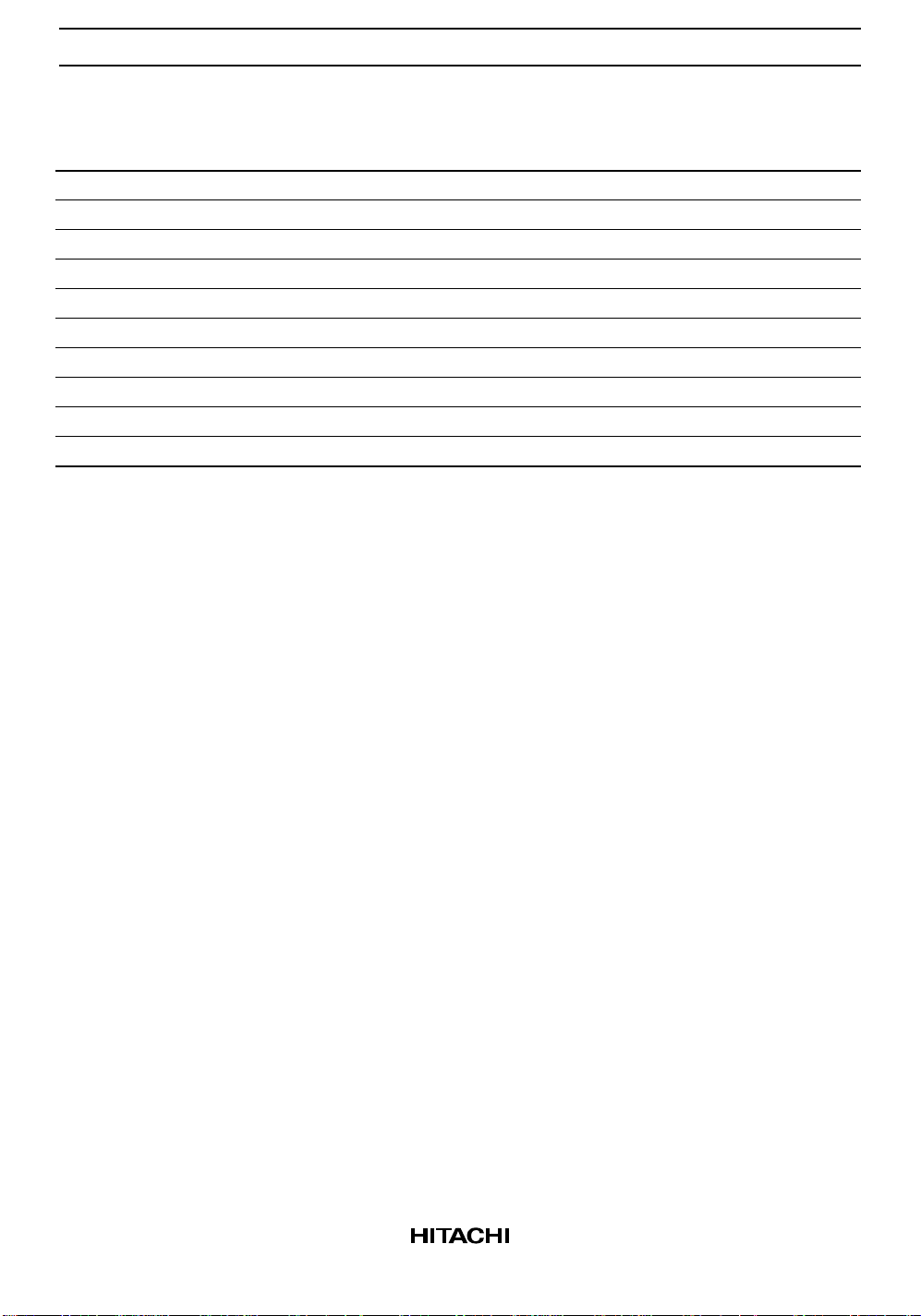
Block Diagram
HD74HC4538
C
X
T
1A
A
A
B
A
C
A
B
DA
T
1B
B
B
C
X
R
X
V
CC
T
2A
Q
A
Q
A
R
X
V
CC
T
2B
Q
B
Q
B
C
DB
RX and CX are external components
3
Page 4
HD74HC4538
Absolute Maximum Ratings
Item Symbol Rating Unit
Supply voltage range V
CC
Input voltage Vin –0.5 to VCC + 0.5 V
Output voltage Vout –0.5 to VCC + 0.5 V
DC input diode current I
DC input diode current pin 2, 14 I
DC output diode current I
IK
IK
OK
DC current drain per pin Iout ±25 mA
DC current drain per VCC, GND ICC, I
Power dissipation per package P
GND
T
Storage temperature Tstg –65 to +150 °C
–0.5 to +7.0 V
±20 mA
±30 mA
±20 mA
±50 mA
500 mW
4
Page 5
HD74HC4538
DC Characteristics
Ta = –40 to
Ta = 25°C
Item Symbol V
Input voltage V
IH
(V) Min Typ Max Min Max Unit Test Conditions
CC
2.0 1.5 — — 1.5 — V
4.5 3.15 — — 3.15 —
6.0 4.2 — — 4.2 —
V
IL
2.0 — — 0.5 — 0.5 V
4.5 — — 1.35 — 1.35
6.0 — — 1.8 — 1.8
Output voltage V
OH
2.0 1.9 2.0 — 1.9 — V Vin = VIH or VILIOH = –20 µA
4.5 4.4 4.5 — 4.4 —
6.0 5.9 6.0 — 5.9 —
4.5 4.18 — — 4.13 — IOH = –4 mA
6.0 5.68 — — 5.63 — IOH = –5.2 mA
V
OL
2.0 — 0.0 0.1 — 0.1 V Vin = VIH or VILIOL = 20 µA
4.5 — 0.0 0.1 — 0.1
6.0 — 0.0 0.1 — 0.1
4.5 — — 0.26 — 0.33 IOL = 4 mA
6.0 — — 0.26 — 0.33 IOL = 5.2 mA
Input current Iin 6.0 — — ±0.1 — ±1.0 µA Vin = VCC or GND
Quiescent supply
I
CC
6.0 — — 130 — 220 µA Vin = VCC or GND,
current
(standby state)
Current drain
I
CC
6.0 — — 130 — 220 µA Vin = VCC or GND,
(active state)
+85°C
Q
= QB = GND, Iout = 0 µA
A
Q
= QB = V
A
CC
Pin 2, 14 = 0.5 V
CC
5
Page 6

HD74HC4538
AC Characteristics (CL = 50 pF, Input tr = tf = 6 ns)
Ta = –40 to
Ta = 25°C
Item Symbol V
Propagation delay t
PLH
(V) Min Typ Max Min Max Unit Test Conditions
CC
2.0 — — 235 — 295 ns A or B to Q
time 4.5 — 22 47 — 59
6.0 — — 40 — 50
t
PHL
2.0 — — 260 — 325 ns A or B to Q
4.5 — 23 52 — 65
6.0 — — 44 — 55
t
PHL
2.0 — — 235 — 295 ns CD to Q
4.5 — 17 47 — 59
6.0 — — 40 — 50
t
PLH
2.0 — — 235 — 295 ns CD to Q
4.5 — — 47 — 59
6.0 — — 40 — 50
Pulse width t
w
2.0 80 — — 100 — ns A, B, C
4.5 16 — — 20 —
6.0 14 — — 17 —
Output pulse width t
WQ
3.0 — 150 — — — ns RX = 1 kΩ, CX = 12 pF
5.0 — 100 — — —
3.0 — — — — — µsRX = 10 kΩ, CX = 100 pF
5.0 — 1.3 — — —
3.0 — — — — — µsRX = 10 kΩ, CX = 1000 pF
5.0 — 9 — — —
3.0 — — — — — µsRX = 10 kΩ, CX = 10000 pF
5.0 — 70 — — —
Pulse width match
∆t
WQ
5.0 — ±0.1 — — — % RX = 10 kΩ, CX = 1000 pF
between circuits in
the same package
Caution in use: In order to prevent any malfunctions due to noise, connect a high frequency performance
capacitor between V
and GND, and keep the wiring between the External components and
CC
Cext, Rext/Cext pins as short as possible.
+85°C
D
6
Page 7

HD74HC4538
Circuit Operation
Fig. 3 shows the HC4538 configured in the retriggerable mode. Briefly, the device operates as follows
(refer to Fig. 1): In the quiescent state, the external timing capacitor, CX, is charged to VCC. When a trigger
occurs, the Q output goes high and CX discharges quickly to the lower references voltage (Vref Lower 1/3
VCC). CX then charges, through RX, back up to the upper reference voltage (Vref Upper 2/3 VCC), at
which point the one-shot has timed out and the Q output goes low.
The following, more detailed description of the circuit operation refers to both the function diagram (Fig. 1)
and the timing diagram (Fig. 2)
Quiescent State
In the quiescent state, before an input trigger appears; the output latch is high and the reset latch is high (1
in Fig. 2). Thus the Q output (pin 6 or 10) of the monostable multivibrator is low (2 Fig. 2).
The output of the trigger-control circuit is low (3), and transistors M1, M2, and M3 are turned off. The
external timing capacitor, CX, is charged to VCC (4), and the upper reference circuit has a low output (5).
Transistor M4 is turned on and analog switch S1 is turned off. Thus the lower reference circuit has VCC at
the noninverting input and a resulting low output (6).
In addition, the output of the trigger-control reset circuit is low.
Trigger Operation
The HC4538 is triggered by either a rising-edge signal as input A (7) or a falling-edge signal at input B (8),
with the unused trigger input and the Reset input held at the voltage levels shown in the Function Table.
Either trigger signal will cause the output of the trigger-control circuit to go high (9). The trigger-control
circuit going high simultaneously initiates three events. First, the output latch goes low, thus taking the Q
output of the HC4538 to a high state (10). Second, transistor M3 is turned on, which allows the external
timing capacitor, CX, to rapidly discharge toward ground (11). (Note that the voltage across CX appears at
the input of the upper reference circuit comparator). Third, transistor M4 is turned off and analog switch
S1 is turned on, thus allowing the voltage across CX to also appear at the input of the lower reference circuit
comparator.
When CX discharges to the reference voltage of the lower reference circuit (12), the outputs of both
reference circuits will be high (13). The trigger-control circuit flip-flop to a low state (14). This turns
transistor M3 off again, allowing CX to begin to charge back up toward VCC, with a time constant t = RXC
(15). In addition, transistor M4 is turned on and analog switch S1 is turned off. Thus a high voltage level
is applied to the input of the lower reference circuit comparator, causing its output to go low (16). The
monostable multivibrator may be retriggered at any time after the trigger-control circuit goes low.
When CX charges up to the reference voltage of the upper reference circuit (17), the output of the upper
reference circuit goes low (18). This causes the output latch to toggle, taking the Q output of the HC4538
to a low state (19), and completing the time-out cycle.
X
7
Page 8

HD74HC4538
Reset Operation
A low voltage applied to the Reset pin always forces the Q output of the HC4538 to a low state.
The timing diagram illustrates the case in which reset occurs (20) while CX is charging up toward the
reference voltage of the upper reference circuit (21). When a reset occurs, the output of the reset latch goes
low (22), turning on transistor M1. Thus CX is allowed to quickly charge up to VCC (23) to await the next
trigger signal.
Retrigger Operation
When used in the retriggerable mode (Fig. 3), the HC4538 may be retriggered during timing out of the
output pulse at any time after the trigger-control circuit flip-flopw has been reset (24). Because the triggercontrol circuit flip-flop resets shortly after CX has discharged to the reference voltage of the lower reference
circuit (25), the minimum retrigger time, trr (Switching Waveform 1) is a function of internal propagation
delays and the discharge time of CX:
Fig. 4 shows the device configured in the non-retriggerable mode.
Power-Down Considerations
Large values of CX may cause problems when powering down the HC4538 because of the amount of
energy stored in the capacitor. When a system containing this device is powered down, the capacitor may
discharge from VCC through the input protection diodes at pin 2 or pin 14. Current through the protection
diodes must be limited to 30 mA; therefore, the turn-off time of the VCC power supply must not be faster
than t = VCC•CX/(30 mA). For example, if VCC = 5 V and CX = 15 µF, the VCC supply must turn off no
faster than t = (5 V)•(15 µF)/30 mA = 2.5 ms. This is usually not a problem because power supplies are
heavily filtered and cannot discharge at this rate.
When a more rapid decrease of VCC to zero voltage occurs, the HC4538 may sustain damage. To avoid this
possibility, use an external clamping diode.
8
Page 9

CX
Q
RX
HD74HC4538
VCC
2, 14
T2
VCC
M2
M1
2kΩ
Upper Reference
Circuit
Output Latch
+
M3
VCC
S1
M
4
–
Vref Upper
Lower Reference
Circuit
6, 10
Q
7, 9
+
–
4, 12
A
B
5, 11
3, 13
D
C
Trigger-Control Circuit
CQ
C
R
Vref Lower
Trigger-Control
Reset Circuit
Reset Latch
Fig. 1 Function Diagram
9
Page 10

HD74HC4538
Trigger Input A
(Pin 4 or 12)
Trigger Input B
(Pin 5 or 11)
Reset Input C
(Pin 3 or 13)
Trigger-Control
Circuit Output
Input
T
2
(Pin 2 or 14)
Upper Reference
Circuit Output
Lower Reference
Circuit Output
Reset Latch
Output
Q Output
(Pin 6 or 10)
D
Quiescent
State
3
4
12
Vref Lower
5
6
1
2
Trigger Cycle (A Input) Trigger Cycle (B Input) Reset
7
8
9
14
11
15
17
13
13
10
Vref Upper
16
19
t
WQ
t
WQ
Retrigger
t
rr
21
24
23
20
25
22
tWQ+t
rr
t
W (H)
A
B
Q
Q
50%
t
W (L)
50%
t
t
PLH
WQ
t
PLH
50%
t
PHL
t
PHL
50%
A
t
rr
B
t
f
10%
90%
10%
50%
t
W (L)
t
PHL
50%
t
PLH
50%
D
C
t
TLH
Q
t
THL
90%
Q
10%
90%
50%
t
r
tWQ+t
rr
50%
(Retriggered Pulse)
Fig. 2 Timing Diagram
10
Page 11

HD74HC4538
Rising-Edge
Trigger
C
X
T
1
A
B
C
D
C
X
T
1
R
X
V
CC
T
2
Q
Q
R
X
V
CC
T
2
Rising-Edge
Trigger
A
B
C
D
Fig. 3 Retriggerable Monostable Circuitry
Q
Q
11
Page 12

HD74HC4538
Falling-Edge
Trigger
C
X
T
1
A
B
C
D
C
X
T
1
A
R
X
V
CC
T
2
Q
Q
R
X
V
CC
T
2
Q
Falling-Edge
Trigger
B
C
D
Fig. 4 Nonritriggerable Monostable Circuitry
Q
12
Page 13

19.20
20.00 Max
16 9
1.3
Unit: mm
6.30
7.40 Max
81
1.11 Max
2.54 ± 0.25
0.48 ± 0.10
5.06 Max
2.54 Min
0.51 Min
Hitachi Code
JEDEC
EIAJ
Weight
7.62
+ 0.13
0.25
– 0.05
0° – 15°
(reference value)
DP-16
Conforms
Conforms
1.07 g
Page 14

16
Unit: mm
10.06
10.5 Max
9
5.5
1
0.80 Max
1.27
*0.42 ± 0.08
0.40 ± 0.06
*Dimension including the plating thickness
Base material dimension
8
0.12
0.10 ± 0.10
0.15
M
2.20 Max
7.80
0.20 ± 0.04
*0.22 ± 0.05
0.70 ± 0.20
Hitachi Code
JEDEC
EIAJ
(reference value)
Weight
+ 0.20
– 0.30
1.15
0° – 8°
FP-16DA
—
Conforms
0.24 g
Page 15

16
Unit: mm
9.9
10.3 Max
9
1
1.27
0.635 Max
*0.42 ± 0.08
0.40 ± 0.06
*Dimension including the plating thickness
Base material dimension
8
0.25
+ 0.11
– 0.04
0.14
0.15
3.95
1.75 Max
M
6.10
1.08
0.20 ± 0.03
*0.22 ± 0.03
+ 0.67
0.60
– 0.20
Hitachi Code
JEDEC
EIAJ
Weight
+ 0.10
– 0.30
0° – 8°
(reference value)
FP-16DN
Conforms
Conforms
0.15 g
Page 16

Cautions
1. Hitachi neither warrants nor grants licenses of any rights of Hitachi’s or any third party’s patent,
copyright, trademark, or other intellectual property rights for information contained in this document.
Hitachi bears no responsibility for problems that may arise with third party’s rights, including
intellectual property rights, in connection with use of the information contained in this document.
2. Products and product specifications may be subject to change without notice. Confirm that you have
received the latest product standards or specifications before final design, purchase or use.
3. Hitachi makes every attempt to ensure that its products are of high quality and reliability. However,
contact Hitachi’s sales office before using the product in an application that demands especially high
quality and reliability or where its failure or malfunction may directly threaten human life or cause risk
of bodily injury, such as aerospace, aeronautics, nuclear power, combustion control, transportation,
traffic, safety equipment or medical equipment for life support.
4. Design your application so that the product is used within the ranges guaranteed by Hitachi particularly
for maximum rating, operating supply voltage range, heat radiation characteristics, installation
conditions and other characteristics. Hitachi bears no responsibility for failure or damage when used
beyond the guaranteed ranges. Even within the guaranteed ranges, consider normally foreseeable
failure rates or failure modes in semiconductor devices and employ systemic measures such as failsafes, so that the equipment incorporating Hitachi product does not cause bodily injury, fire or other
consequential damage due to operation of the Hitachi product.
5. This product is not designed to be radiation resistant.
6. No one is permitted to reproduce or duplicate, in any form, the whole or part of this document without
written approval from Hitachi.
7. Contact Hitachi’s sales office for any questions regarding this document or Hitachi semiconductor
products.
Hitachi, Ltd.
Semiconductor & Integrated Circuits.
Nippon Bldg., 2-6-2, Ohte-machi, Chiyoda-ku, Tokyo 100-0004, Japan
Tel: Tokyo (03) 3270-2111 Fax: (03) 3270-5109
URL NorthAmerica : http:semiconductor.hitachi.com/
For further information write to:
Hitachi Semiconductor
(America) Inc.
179 East Tasman Drive,
San Jose,CA 95134
Tel: <1> (408) 433-1990
Fax: <1>(408) 433-0223
Europe : http://www.hitachi-eu.com/hel/ecg
Asia (Singapore) : http://www.has.hitachi.com.sg/grp3/sicd/index.htm
Asia (Taiwan) : http://www.hitachi.com.tw/E/Product/SICD_Frame.htm
Asia (HongKong) : http://www.hitachi.com.hk/eng/bo/grp3/index.htm
Japan : http://www.hitachi.co.jp/Sicd/indx.htm
Hitachi Europe GmbH
Electronic components Group
Dornacher Stra§e 3
D-85622 Feldkirchen, Munich
Germany
Tel: <49> (89) 9 9180-0
Fax: <49> (89) 9 29 30 00
Hitachi Europe Ltd.
Electronic Components Group.
Whitebrook Park
Lower Cookham Road
Maidenhead
Berkshire SL6 8YA, United Kingdom
Tel: <44> (1628) 585000
Fax: <44> (1628) 778322
Hitachi Asia Pte. Ltd.
16 Collyer Quay #20-00
Hitachi Tower
Singapore 049318
Tel: 535-2100
Fax: 535-1533
Hitachi Asia Ltd.
Taipei Branch Office
3F, Hung Kuo Building. No.167,
Tun-Hwa North Road, Taipei (105)
Tel: <886> (2) 2718-3666
Fax: <886> (2) 2718-8180
Copyright ' Hitachi, Ltd., 1999. All rights reserved. Printed in Japan.
Hitachi Asia (Hong Kong) Ltd.
Group III (Electronic Components)
7/F., North Tower, World Finance Centre,
Harbour City, Canton Road, Tsim Sha Tsui,
Kowloon, Hong Kong
Tel: <852> (2) 735 9218
Fax: <852> (2) 730 0281
Telex: 40815 HITEC HX
 Loading...