

Page 1

HD74HC4052/HD74HC4053
Dual 4-channel Analog Multiplexers/Demultiplexers/
Triple 2-channel Analog Multiplexers/Demultiplexers
Description
HD74HC4052: This device connects together the outputs of 4 switches in two sets, thus achieving a pair of
4 channel multiplexers. The binary code placed on the A, and B select lines determine which switch in
each 4 channel section is “on”, connecting one of the four inputs in each section to its common output.
This enables the implementation of a 4 channel differential multiplexer.
HD74HC4053: This device contains 6 switches whose outputs are connected together in pairs, thus
implementing a triple 2 channel multiplexer, or the equivalent of 3 single-pole-double throw configuration.
Each of the A, B, or C select lines independently controls one pair of switches, selecting one of the two
switches to be “on”.
Features
• High Speed Operation
• Wide Operating Voltage
• Low Quiescent Supply Current
Page 2
HD74HC4052/HD74HC4053
Function Table
Control Inputs
Select ON Switch
Inhibit C*
LLLLY
LL L H Y
LL H L Y
LL HHY
LH L L Z
LH L H Z
LH H L Z
LH H H Z
HXXX— —
Note: 1. Not applicable for HD74HC4052
1
B A HD74HC4052 HD74HC4053
X = Dont’t Care
0
1
2
3
X
0
X
1
X
2
X
3
Z
0
Z
0
Z
0
Z
0
1
1
1
1
Y
0
Y
0
Y
1
Y
1
Y
0
Y
0
Y
1
Y
1
X
0
X
1
X
0
X
1
X
0
X
1
X
0
X
1
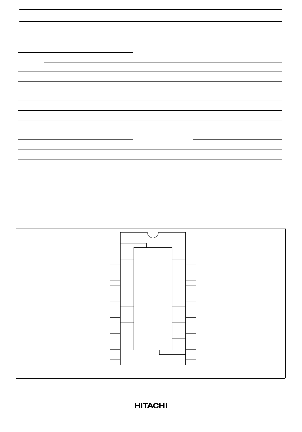
Pin Arrangement
HD74HC4052
Y
Y
Y
Y
Inhibit
V
EE
GND
1
0
Y
2
2
Y
3
4
3
5
1
6
Y
2
Y
Y
3
Y
1
Inhibit
7
0
X
2
X
1
X
X
0
X
3
A
16
15
14
13
12
11
10
V
CC
X
2
X
1
X
X
0
X
3
A
B
B
8
9
(Top view)
2
Page 3
HD74HC4053
HD74HC4052/HD74HC4053
Block Diagram
HD74HC4052
Y
Y
Z
Z
Inhibit
V
EE
GND
1
1
Y
2
0
3
1
Z
4
5
0
6
Y
0
Z
1
Z
Z
0
Inhibit
7
1
Y
X
X
1
X
0
A
B
16
15
14
13
12
11
10
V
CC
Y
X
X
1
X
0
A
B
C
C
8
9
(Top view)
Inh
X
X
X
X
Y
Y
Y
Y
V
CC
A
B
0
1
2
3
0
1
2
3
Level
Converter
GND V
EE
Binary to
1-of-4 Decoder
with Inhibit
X
Y
3
Page 4
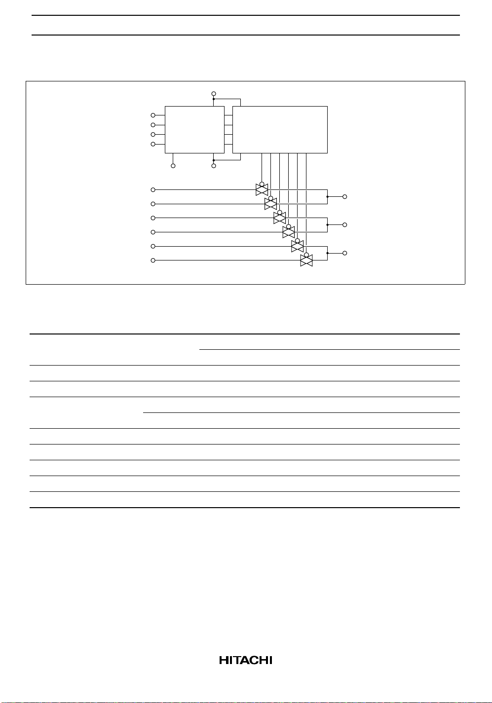
HD74HC4052/HD74HC4053
HD74HC4053
V
CC
Inh
X
X
Y
Y
Z
Z
A
B
C
0
1
0
1
0
1
Level
Converter
GND V
EE
Binary to 1-of-2
Decoder with
Inhibit
X
Y
Z
Absolute Maximum Ratings
Item Symbol Rating Unit
Supply voltage V
Control input voltage V
Switch I/O voltage V
Supply current (VCC)I
(GND) I
Switch I/O current (per pin) I
Control input diode current I
Switch I/O diode current I
Power dissipation P
CC
VCC – V
IN
I/O
CC
GND
I/O
IK
IOK
T
EE
Storage temperature range Tstg –65 to +150 °C
–0.5 to +7.0 V
–0.5 to +7.0 V
GND – 0.5 to VCC + 0.5 V
VEE –0.5 to VCC + 0.5 V
+50 mA
–50 mA
±25 mA
±20 mA
±20 mA
500 mW
4
Page 5
HD74HC4052/HD74HC4053
Recommended Operating Range
Item Symbol Min Typ Max Unit
Supply voltage V
CC
– V
GND – V
Control input voltage V
Switch I/O voltage V
IN
I/O
Operating temperature Topr –40 — +85 °C
Input rise/fall time VCC = 2.0 V tr, t
f
VCC = 4.5 V 0 — 500 ns
VCC = 6.0 V 0 — 400 ns
2—6V
EE
–4 — 0 V
EE
0—VCCV
V
EE
—VCCV
0 — 1000 ns
5
Page 6

HD74HC4052/HD74HC4053
DC Characteristics (VSS = VEE = GND)
Ta = –40 to
Ta = 25°C
Item Symbol V
Control input voltage V
IH
(V) Min Typ Max Min Max Unit Test Conditions
CC
2.0 1.5 — — 1.5 — V
4.5 3.15 — — 3.15 —
6.0 4.2 — — 4.2 —
V
IL
2.0 — — 0.5 — 0.5 V
4.5 — — 1.35 — 1.35
6.0 — — 1.8 — 1.8
ON resistance R
ON
2.0 — 2000 5000 — 6250 Ω V
4.5 — 120 180 — 225 V
6.0 — 100 170 — 210 I
2.0 — 200 800 — 1000 Ω V
4.5 — 80 150 — 190 V
6.0 — 70 140 — 175 V
∆ON resistance ∆R
ON
2.0 —50———Ω V
between any two 4.5 — 13 40 — 50 V
channels 6.0 — 10 20 — 25 I
OFF channel
I
S (OFF)
6.0 — — ±0.1 — ±1.0 µAV
leakage current
(switch off)
OFF channel
I
S (ON)
6.0 — — ±0.1 — ±1.0 µAV
leakage current
(switch on)
Control input current Iin 6.0 — — ±0.1 — ±1.0 µA Vin = VCC or V
Quiescent supply
I
CC
6.0 — — 4.0 — 40 µA Vin = VCC or V
current
+85°C
= V
INH
= VCC to V
I/O
≤ 2 mA
I/O
= V
INH
= VCC to V
I/O
≤ 2 mA
I/O
= V
INH
= VCC to V
I/O
≤ 2 mA
I/O
= V
INH
= V
INH
IL
IL
IL
IL
IL
EE
EE
EE
SS
SS
6
Page 7

HD74HC4052/HD74HC4053
AC Characteristics (CL = 50 pF, Input tr = tf = 6 ns, VSS = VEE = GND)
Ta = –40 to
Ta = 25°C
Item Symbol V
Propagation delay t
PLH
(V) Min Typ Max Min Max Unit Test Conditions
CC
2.0 — 25 60 — 75 ns RL = 10 kΩ
time 4.5 — 6 12 — 15 Switch input to
6.0 — 5 10 — 13 switch output
t
PHL
2.0 — 25 60 — 75 ns
4.5 — 6 12 — 15
6.0 — 5 10 — 13
Propagation delay t
PLH
2.0 — 50 153 — 191 ns RL = 10 kΩ
time 4.5 — 16 30 — 38 Control input to
6.0 — 14 26 — 33 switch output
t
PHL
2.0 — 50 153 — 191 ns
4.5 — 16 30 — 38
6.0 — 14 26 — 33
Output enable t
ZH
2.0 — 50 153 — 191 ns RL = 1 kΩ
time 4.5 — 14 30 — 38
6.0 — 12 26 — 33
t
ZL
2.0 — 50 153 — 191 ns
4.5 — 14 30 — 38
6.0 — 12 26 — 33
Output disable t
HZ
2.0 — 40 153 — 191 ns RL = 1 kΩ
time 4.5 — 17 30 — 38
6.0 — 14 26 — 33
t
LZ
2.0 — 40 153 — 191 ns
4.5 — 17 30 — 38
6.0 — 14 26 — 33
Control input
Cin — — 5 10 — 10 pF
capacitance
Switch input
Cin 5.0 — 5 — — — pF
capacitance
Output capacitance Cout 5.0 — 12 — — — pF HD74HC4052
(Common pin) 5.0 — 6 — — — HD74HC4053
Feed through Cin–out 5.0 — 0.6 — — — pF HD74HC4052
capacitance 5.0 — 0.5 — — — HD74HC4053
+85°C
7
Page 8

HD74HC4052/HD74HC4053
AC Characteristics (CL = 50 pF, Input tr = tf = 6 ns, VSS = VEE = GND) (cont)
Ta = –40 to
Ta = 25°C
Item Symbol V
Power dissipation C
PD
(V) Min Typ Max Min Max Unit Test Conditions
CC
5.0 — 32.0 — — — pF HD74HC4052
capacitance 5.0 — 17.0 — — — HD74HC4053
Sine wave distortion 4.5 — 0.1 — — — % fin = 1 kHz, Vin = 4 V
Frequency response
4.5 — 95 — — — MHz fin = 1 MHz,
channel “ON”
(Sine wave input)
Feed through
4.5 — –50 — — — dB RL = 600 Ω, CL = 50 pF,
attenuation
Cross talk between 2.0 — 25 — — — mV RL = 600 Ω, CL = 15 pF,
control input and 4.5 — 50 — — — fin = 1 MHz
switch I/O 6.0 — 75 — — —
Cross talk between
4.5 — 50 — — — dB RL = 600 Ω, CL = 50 pF,
any two switches
Maximum control 2.0 — 20 — — — MHz RL = 1 kΩ, CL = 15 pF
frequency 4.5 — 30 — — — Vout = 1/2 (VCC)
6.0 —30———
+85°C
RL = 10 kΩ, CL = 50 pF
P-P
20 log
10 VOS/VIS
R
= 50 Ω, CL = 10 pF
L
f
= 1 MHz
in
f
= 1 MHz
in
= –3 dB
AC Characteristics Test Circuit
Maximum Control Frequency
V
EE
CC
V
CC
V
out
V
SS
RL=
1kΩ
V
in • VCC
8
V
C
V
CL=
15pF
V
CC
V
C
0 V
V
out
Vcc/2
Page 9

Cross talk (Between Any Two Switches)
V
CC
V
EE
CC
CC
(ON)
CC
V
SS
V
out2
V
Rin=
600Ω
in
V
f
in
0.1µF
V
V
(OFF)
V
out1
VCC/2
RL=
600Ω
HD74HC4052/HD74HC4053
V
CL=
50pF
in
(Sine Wave)
(V
=0dBm,f=1MHz)
in
Rin=
600Ω
V
EE
V
SS
RL=
600Ω
VCC/2
Cross talk (Control Input to Switch Output)
V
EE
CC
V
CC
V
out
V
SS
RL=
600Ω
V
C
V
in
Rin=
600Ω
V
VCC/2 VCC/2
Feed through Attenuation
V
CC
V
EE
(OFF)
CC
V
out
V
SS
0.1µF
f
in
Rin=
600Ω
V
in
V
VCC/2 VCC/2
RL=
600Ω
CL=
50pF
CL=
50pF
CL=
50pF
t
r
V
CC
V
SS
90%
10%
(f=1MHz)
t
=6ns
r=tr
V
in
t
f
(Sine Wave)
=0dBm,f=1MHz)
(V
in
9
Page 10

HD74HC4052/HD74HC4053
Sine Wave Distortion
V
CC
V
V
10µF
in
V
f
in
Cin, Cout, Cin–out (Input, Output and Feed through Capacitance)
CC
(ON)
EE
V
out
V
SS
RL=
10kΩ
CL=
50pF
VCC/2
C
C
in-out
in-out
5V
5V
V
V
CC
CC
Input Pin Commom Pin
C
C
in
in
(OFF)
(OFF)
V
V
EE
EE
V
V
SS
SS
V
in
(Sine Wave)
Commom Pin
C
C
out
out
(V
=4V
,f=1kHz)
in
p-p
Frequency Response Channel ON
V
CC
V
EE
(ON)
CC
V
SS
V
0.1µF
in
V
f
in
V
out
VCC/2
RL=
50Ω
CL=
10pF
f
in
(Sine Wave)
=0dBm,f=1MHz)
(V
out
10
Page 11

RON: ON Resistance
V
CC
V
EE
(ON)
CC
V
SS
V
I/O
in
V
IS (OFF): OFF Channel Leakage Current (Switch OFF)
HD74HC4052/HD74HC4053
O/I
V
V
I-O
V
CC
V
out
V
in=VCC
or V
SS
I/O
A
V
EE
IS (ON): OFF Channel Leakage Current (Switch ON)
V
in=VCC
or V
SS
I/O
A
V
EE
V
(OFF)
(ON)
CC
V
V
V
CC
CC
SS
V
SS
V
out=VSS
or V
V
out
OPEN
CC
11
Page 12

HD74HC4052/HD74HC4053
t
, t
PLH
: Propagation Delay Time (Switch Input to Switch Output)
PHL
V
CC
V
CC
V
in
t
, t
PLH
PHL
VC=V
V
CC or VSS
(Switch Input)
V
SS or VCC
(ON)
V
V
EE
SS
RL=
10kΩ
CL=
50pF
V
out
: Propagation Delay Time (Control Input to Switch Output)
V
in
V
CC
V
CC
V
EE
SS
RL=
10kΩ
CL=
50pF
tZH, tZL/tHZ, tLZ: Output Enable and Disable Time
V
out
Common Pin
50%
t
f
10%
t
PHL
t
PHL
t
r
V
CC
V
in
V
SS
V
OH
V
out
V
OL
V
CC
V
C
V
SS
V
OH
V
out
V
OL
t
PLH
t
90%
50%
50%
PLH
50%
V
INH =Vin
VCCV
t
f
V
V
CC
V
CC
V
V
EE
SS
RL=
1kΩ
SS
VSSV
CC
CL=
50pF
V
out
V
V
V
INH
out
out
CC
V
SS
V
OH
V
OL
V
OH
V
OL
90%
50%
10%
t
ZH
50%
t
ZL
50%
t
r
t
HZ
90%
t
LZ
10%
12
Page 13

19.20
20.00 Max
16 9
1.3
Unit: mm
6.30
7.40 Max
81
1.11 Max
2.54 ± 0.25
0.48 ± 0.10
5.06 Max
2.54 Min
0.51 Min
Hitachi Code
JEDEC
EIAJ
Weight
7.62
+ 0.13
0.25
– 0.05
0° – 15°
(reference value)
DP-16
Conforms
Conforms
1.07 g
Page 14

16
Unit: mm
10.06
10.5 Max
9
5.5
1
0.80 Max
1.27
*0.42 ± 0.08
0.40 ± 0.06
*Dimension including the plating thickness
Base material dimension
8
0.12
0.10 ± 0.10
0.15
M
2.20 Max
7.80
0.20 ± 0.04
*0.22 ± 0.05
0.70 ± 0.20
Hitachi Code
JEDEC
EIAJ
(reference value)
Weight
+ 0.20
– 0.30
1.15
0° – 8°
FP-16DA
—
Conforms
0.24 g
Page 15

16
Unit: mm
9.9
10.3 Max
9
1
1.27
0.635 Max
*0.42 ± 0.08
0.40 ± 0.06
*Dimension including the plating thickness
Base material dimension
8
0.25
+ 0.11
– 0.04
0.14
0.15
3.95
1.75 Max
M
6.10
1.08
0.20 ± 0.03
*0.22 ± 0.03
0.60
Hitachi Code
JEDEC
EIAJ
Weight
+ 0.10
– 0.30
0° – 8°
+ 0.67
– 0.20
(reference value)
FP-16DN
Conforms
Conforms
0.15 g
Page 16

Cautions
1. Hitachi neither warrants nor grants licenses of any rights of Hitachi’s or any third party’s patent,
copyright, trademark, or other intellectual property rights for information contained in this document.
Hitachi bears no responsibility for problems that may arise with third party’s rights, including
intellectual property rights, in connection with use of the information contained in this document.
2. Products and product specifications may be subject to change without notice. Confirm that you have
received the latest product standards or specifications before final design, purchase or use.
3. Hitachi makes every attempt to ensure that its products are of high quality and reliability. However,
contact Hitachi’s sales office before using the product in an application that demands especially high
quality and reliability or where its failure or malfunction may directly threaten human life or cause risk
of bodily injury, such as aerospace, aeronautics, nuclear power, combustion control, transportation,
traffic, safety equipment or medical equipment for life support.
4. Design your application so that the product is used within the ranges guaranteed by Hitachi particularly
for maximum rating, operating supply voltage range, heat radiation characteristics, installation
conditions and other characteristics. Hitachi bears no responsibility for failure or damage when used
beyond the guaranteed ranges. Even within the guaranteed ranges, consider normally foreseeable
failure rates or failure modes in semiconductor devices and employ systemic measures such as failsafes, so that the equipment incorporating Hitachi product does not cause bodily injury, fire or other
consequential damage due to operation of the Hitachi product.
5. This product is not designed to be radiation resistant.
6. No one is permitted to reproduce or duplicate, in any form, the whole or part of this document without
written approval from Hitachi.
7. Contact Hitachi’s sales office for any questions regarding this document or Hitachi semiconductor
products.
Hitachi, Ltd.
Semiconductor & Integrated Circuits.
Nippon Bldg., 2-6-2, Ohte-machi, Chiyoda-ku, Tokyo 100-0004, Japan
Tel: Tokyo (03) 3270-2111 Fax: (03) 3270-5109
URL NorthAmerica : http:semiconductor.hitachi.com/
For further information write to:
Hitachi Semiconductor
(America) Inc.
179 East Tasman Drive,
San Jose,CA 95134
Tel: <1> (408) 433-1990
Fax: <1>(408) 433-0223
Europe : http://www.hitachi-eu.com/hel/ecg
Asia (Singapore) : http://www.has.hitachi.com.sg/grp3/sicd/index.htm
Asia (Taiwan) : http://www.hitachi.com.tw/E/Product/SICD_Frame.htm
Asia (HongKong) : http://www.hitachi.com.hk/eng/bo/grp3/index.htm
Japan : http://www.hitachi.co.jp/Sicd/indx.htm
Hitachi Europe GmbH
Electronic components Group
Dornacher Stra§e 3
D-85622 Feldkirchen, Munich
Germany
Tel: <49> (89) 9 9180-0
Fax: <49> (89) 9 29 30 00
Hitachi Europe Ltd.
Electronic Components Group.
Whitebrook Park
Lower Cookham Road
Maidenhead
Berkshire SL6 8YA, United Kingdom
Tel: <44> (1628) 585000
Fax: <44> (1628) 778322
Hitachi Asia Pte. Ltd.
16 Collyer Quay #20-00
Hitachi Tower
Singapore 049318
Tel: 535-2100
Fax: 535-1533
Hitachi Asia Ltd.
Taipei Branch Office
3F, Hung Kuo Building. No.167,
Tun-Hwa North Road, Taipei (105)
Tel: <886> (2) 2718-3666
Fax: <886> (2) 2718-8180
Copyright ' Hitachi, Ltd., 1999. All rights reserved. Printed in Japan.
Hitachi Asia (Hong Kong) Ltd.
Group III (Electronic Components)
7/F., North Tower, World Finance Centre,
Harbour City, Canton Road, Tsim Sha Tsui,
Kowloon, Hong Kong
Tel: <852> (2) 735 9218
Fax: <852> (2) 730 0281
Telex: 40815 HITEC HX
 Loading...