

Page 1

HD74AC539
Dual 1-of-4 Decoder with 3-State Output
Description
The HD74AC539 contains two inpedendent decoders. Each accepts two Address (A0, A1) input signals and
decodes them to select one of four mutually exclusive outputs. A polarity control input (P) determines
whether the outputs are active HIGH (P = L) or active LOW (P = H). An active LOW input Enable (E) is
available for data demultiplexing; data is routed to the selected output in non-inverted form in the active
LOW mode or in inverted form in the active HIGH mode. A HIGH signal on the active LOW Output
Enable (OE) input forces the 3-state outputs to the high impedance state.
Feature
• Outputs Source/Sink 24 mA
Page 2
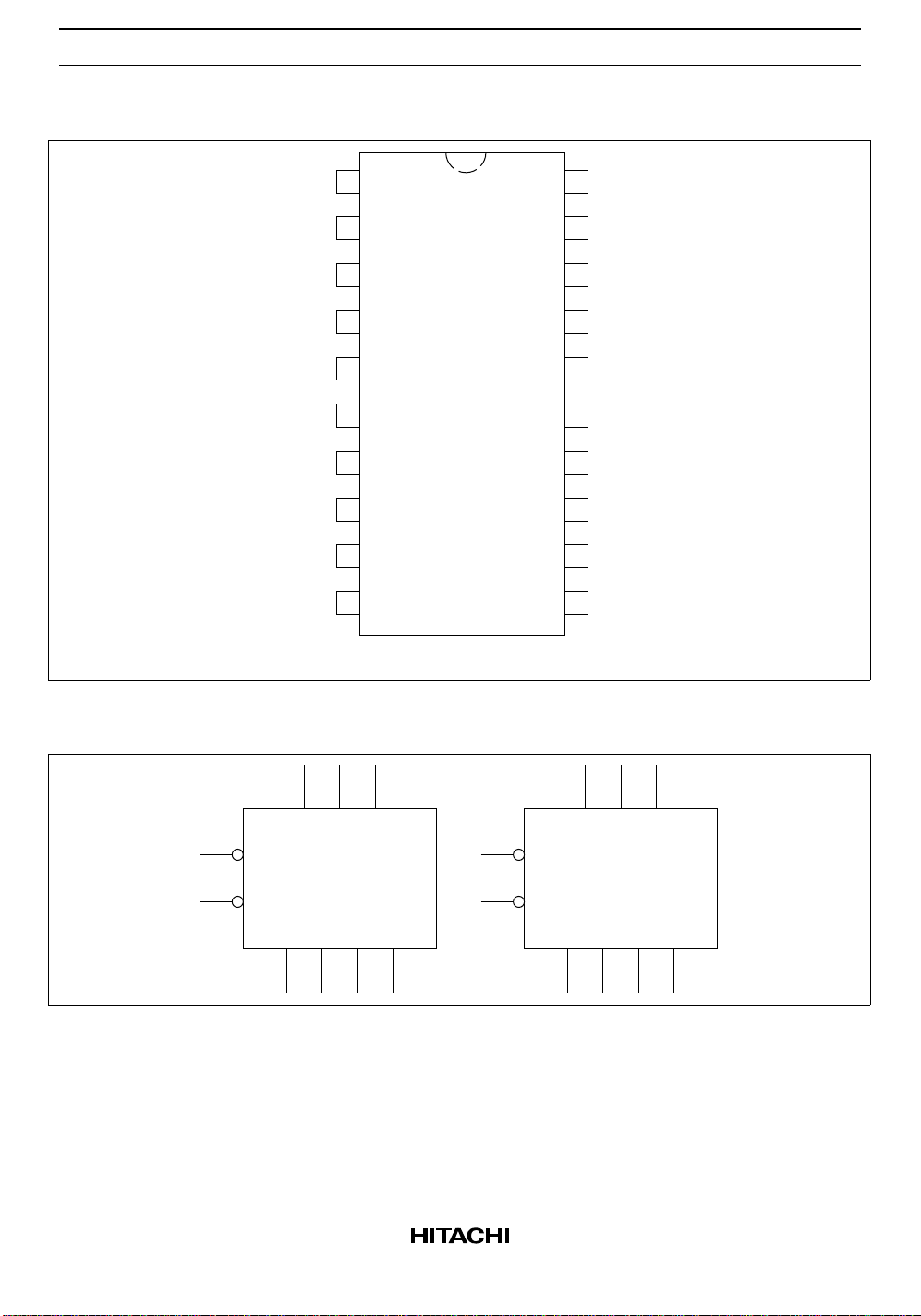
HD74AC539
Pin Arrangement
O2b
1
20
V
CC
Logic Symbol
2
O1b
O0b
3
Pb
4
OEb
5
A0a
6
7
A1a
O3a
8
O2a
9
GND
10 11
(Top view)
19
18
17
16
15
14
13
12
O3b
A1b
A0b
Eb
Ea
OE
Pa
O0d
O1a
a
P
A0
A1
E
DECODER a
OE
O0 O1 O2 O3
2
P
A0
E
DECODER b
OE
O0 O1 O2 O3
A1
Page 3
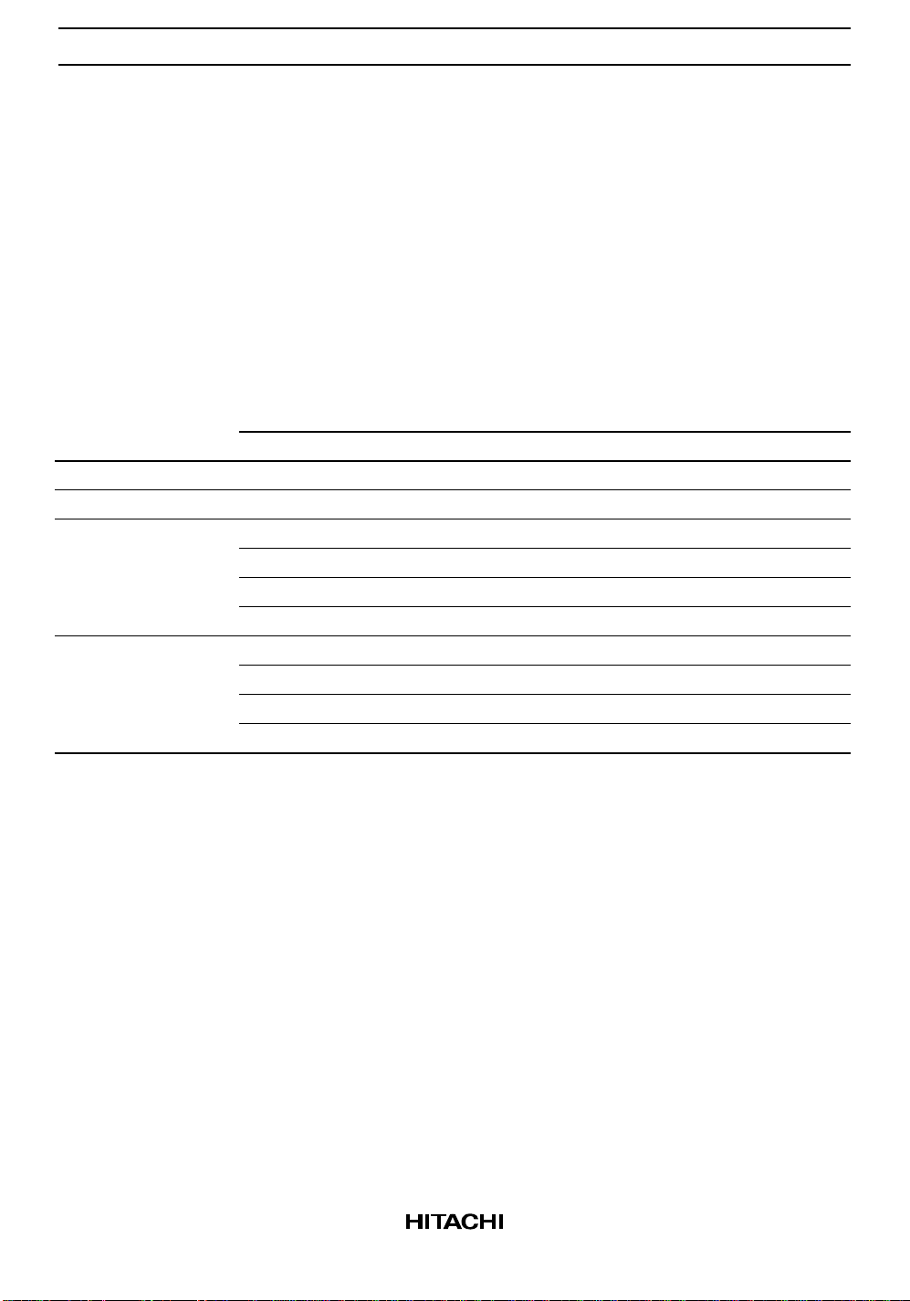
Pin Names
HD74AC539
A0a to A
A0b to A
Ea – E
b
OEa, OE
Pa, P
b
O0a to O
O0b to O
1a
1b
b
3a
3b
Side A Address Inputs
Side B Address Inputs
Enable Inputs (Active LOW)
Output Enable Inputs (Active LOW)
Polarity Control Inputs
Side A 3-State Outputs
Side B 3-State Outputs
Truth Table
Inputs Outputs
Function OE E A
1
A
0
High impedance H X X X ZZZZ
Disable L H X X On = P
Active HIGH output LLLLHLLL
(P = L) LLLHLHLL
LLHLLLHL
LLHHLLLH
Active LOW output LLLLLHHH
(P = H) LLLHHLHH
LLHLHHLH
LLHH HHHL
H : High Voltage Level
L : Low Voltage Level
X : Immaterial
Z : High Impedance
O
0
O
1
O
2
O
3
3
Page 4
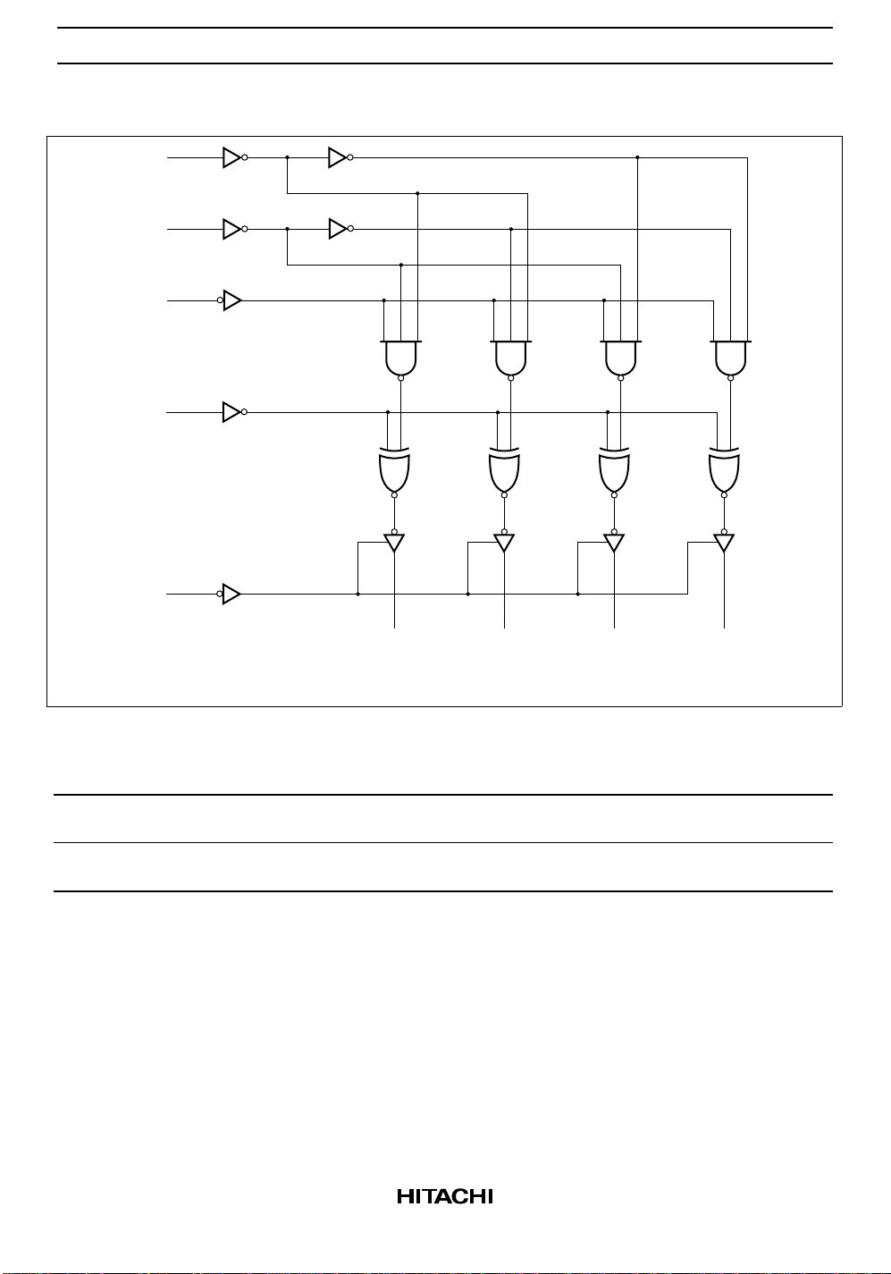
HD74AC539
Logic Diagram (one half shown)
A1
A0
E
P
OE
O0 O1 O2 O3
Please note that this diagram is provided only for the understanding of logic operations and should not be
used to estimate propagation delays.
DC Characteristics (unless otherwise specified)
Item Symbol Max Unit Condition
Maximum quiescent supply current I
Maximum quiescent supply current I
CC
CC
80 µAV
8.0 µAV
= VCC or ground, VCC = 5.5 V,
IN
Ta = Worst case
= VCC or ground, VCC = 5.5 V,
IN
Ta = 25°C
4
Page 5
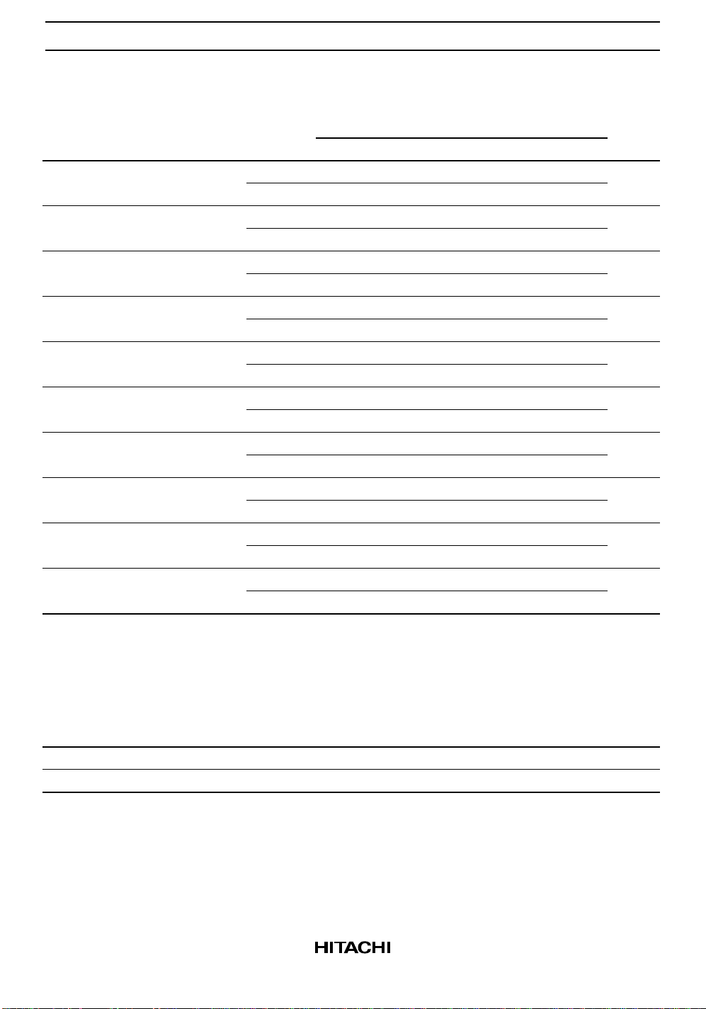
AC Characteristics: HD74AC539
HD74AC539
Item Symbol V
Propagation delay t
An to O
n
Propagation delay t
An to O
n
Propagation delay t
E to O
n
Propagation delay t
E to O
n
Propagation delay t
P to O
n
Propagation delay t
P to O
n
Propagation delay t
OE to O
n
Propagation delay t
OE to O
n
Propagation delay t
OE to O
n
Propagation delay t
OE to O
n
PLH
PHL
PLH
PHL
PLH
PHL
ZH
ZL
HZ
LZ
(V)*1Min Typ Max Min Max Unit
CC
3.3 1.0 — 15.0 1.0 18.0 ns
5.0 1.0 — 10.0 1.0 12.0
3.3 1.0 — 15.0 1.0 18.0 ns
5.0 1.0 — 10.0 1.0 12.0
3.3 1.0 — 14.5 1.0 16.5 ns
5.0 1.0 — 9.5 1.0 11.0
3.3 1.0 — 13.5 1.0 15.5 ns
5.0 1.0 — 9.0 1.0 11.5
3.3 1.0 — 16.0 1.0 19.0 ns
5.0 1.0 — 11.5 1.0 12.5
3.3 1.0 — 16.0 1.0 19.0 ns
5.0 1.0 — 11.5 1.0 12.5
3.3 1.0 — 10.0 1.0 11.5 ns
5.0 1.0 — 8.0 1.0 9.0
3.3 1.0 — 9.5 1.0 11.0 ns
5.0 1.0 — 7.5 1.0 8.5
3.3 1.0 — 11.5 1.0 13.0 ns
5.0 1.0 — 9.5 1.0 10.5
3.3 1.0 — 10.5 1.0 12.0 ns
5.0 1.0 — 8.5 1.0 9.5
Note: 1. Voltage Range 3.3 is 3.3 V ± 0.3 V
Voltage Range 5.0 is 5.0 V ± 0.5 V
Ta = +25°C
C
= 50 pF
L
Ta = –40°C to +85°C
CL = 50 pF
Capacitance
Item Symbol Typ Unit Condition
Input capacitance C
Power dissipation capacitance C
IN
PD
4.5 pF VCC = 5.5 V
60 pF VCC = 5.0 V
5
Page 6
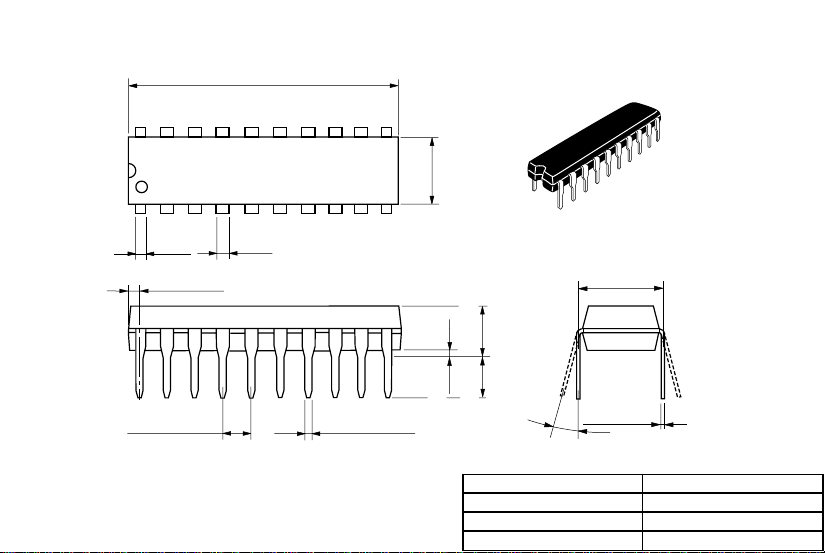
24.50
25.40 Max
Unit: mm
1120
6.30
1
0.89
1.27 Max
2.54 ± 0.25
1.30
10
0.48 ± 0.10
7.00 Max
0.51 Min
2.54 Min 5.08 Max
Hitachi Code
JEDEC
EIAJ
Weight
7.62
+ 0.11
0.25
– 0.05
0° – 15°
(reference value)
DP-20N
—
Conforms
1.26 g
Page 7
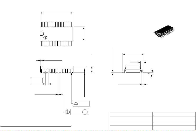
20
Unit: mm
12.6
13 Max
11
5.5
1
0.80 Max
1.27
*0.42 ± 0.08
0.40 ± 0.06
*Dimension including the plating thickness
Base material dimension
10
0.12
0.10 ± 0.10
0.15
M
2.20 Max
7.80
0.20 ± 0.04
*0.22 ± 0.05
0.70 ± 0.20
Hitachi Code
JEDEC
EIAJ
Weight
(reference value)
+ 0.20
– 0.30
1.15
0° – 8°
FP-20DA
—
Conforms
0.31 g
Page 8
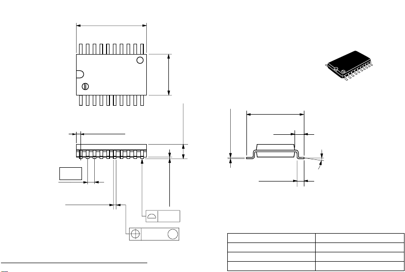
20
Unit: mm
12.8
13.2 Max
11
7.50
1
0.935 Max
1.27
*0.42 ± 0.08
0.40 ± 0.06
*Dimension including the plating thickness
Base material dimension
10
0.12
0.20 ± 0.10
0.15
2.65 Max
M
10.40
0.25 ± 0.04
*0.27 ± 0.05
0.70
Hitachi Code
JEDEC
EIAJ
Weight
+ 0.25
– 0.40
1.45
+ 0.57
– 0.30
(reference value)
0° – 8°
FP-20DB
Conforms
—
0.52 g
Page 9
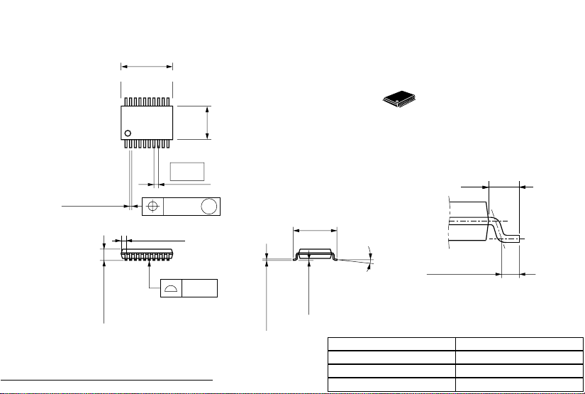
20 11
110
+0.08
*0.22
–0.07
0.20 ± 0.06
6.50
6.80 Max
0.65 Max
0.65
0.13
Unit: mm
4.40
1.0
M
6.40 ± 0.20
0.10
1.10 Max
*Dimension including the plating thickness
Base material dimension
0.15 ± 0.04
*0.17 ± 0.05
+0.03
–0.04
0.07
0° – 8°
Hitachi Code
JEDEC
EIAJ
(reference value)
Weight
0.50 ± 0.10
TTP-20DA
—
—
0.07 g
Page 10
Cautions
1. Hitachi neither warrants nor grants licenses of any rights of Hitachi’s or any third party’s patent,
copyright, trademark, or other intellectual property rights for information contained in this document.
Hitachi bears no responsibility for problems that may arise with third party’s rights, including
intellectual property rights, in connection with use of the information contained in this document.
2. Products and product specifications may be subject to change without notice. Confirm that you have
received the latest product standards or specifications before final design, purchase or use.
3. Hitachi makes every attempt to ensure that its products are of high quality and reliability. However,
contact Hitachi’s sales office before using the product in an application that demands especially high
quality and reliability or where its failure or malfunction may directly threaten human life or cause risk
of bodily injury, such as aerospace, aeronautics, nuclear power, combustion control, transportation,
traffic, safety equipment or medical equipment for life support.
4. Design your application so that the product is used within the ranges guaranteed by Hitachi particularly
for maximum rating, operating supply voltage range, heat radiation characteristics, installation
conditions and other characteristics. Hitachi bears no responsibility for failure or damage when used
beyond the guaranteed ranges. Even within the guaranteed ranges, consider normally foreseeable
failure rates or failure modes in semiconductor devices and employ systemic measures such as failsafes, so that the equipment incorporating Hitachi product does not cause bodily injury, fire or other
consequential damage due to operation of the Hitachi product.
5. This product is not designed to be radiation resistant.
6. No one is permitted to reproduce or duplicate, in any form, the whole or part of this document without
written approval from Hitachi.
7. Contact Hitachi’s sales office for any questions regarding this document or Hitachi semiconductor
products.
Hitachi, Ltd.
Semiconductor & Integrated Circuits.
Nippon Bldg., 2-6-2, Ohte-machi, Chiyoda-ku, Tokyo 100-0004, Japan
Tel: Tokyo (03) 3270-2111 Fax: (03) 3270-5109
URL NorthAmerica : http:semiconductor.hitachi.com/
For further information write to:
Hitachi Semiconductor
(America) Inc.
179 East Tasman Drive,
San Jose,CA 95134
Tel: <1> (408) 433-1990
Fax: <1>(408) 433-0223
Europe : http://www.hitachi-eu.com/hel/ecg
Asia (Singapore) : http://www.has.hitachi.com.sg/grp3/sicd/index.htm
Asia (Taiwan) : http://www.hitachi.com.tw/E/Product/SICD_Frame.htm
Asia (HongKong) : http://www.hitachi.com.hk/eng/bo/grp3/index.htm
Japan : http://www.hitachi.co.jp/Sicd/indx.htm
Hitachi Europe GmbH
Electronic components Group
Dornacher Stra§e 3
D-85622 Feldkirchen, Munich
Germany
Tel: <49> (89) 9 9180-0
Fax: <49> (89) 9 29 30 00
Hitachi Europe Ltd.
Electronic Components Group.
Whitebrook Park
Lower Cookham Road
Maidenhead
Berkshire SL6 8YA, United Kingdom
Tel: <44> (1628) 585000
Fax: <44> (1628) 778322
Hitachi Asia Pte. Ltd.
16 Collyer Quay #20-00
Hitachi Tower
Singapore 049318
Tel: 535-2100
Fax: 535-1533
Hitachi Asia Ltd.
Taipei Branch Office
3F, Hung Kuo Building. No.167,
Tun-Hwa North Road, Taipei (105)
Tel: <886> (2) 2718-3666
Fax: <886> (2) 2718-8180
Copyright ' Hitachi, Ltd., 1999. All rights reserved. Printed in Japan.
Hitachi Asia (Hong Kong) Ltd.
Group III (Electronic Components)
7/F., North Tower, World Finance Centre,
Harbour City, Canton Road, Tsim Sha Tsui,
Kowloon, Hong Kong
Tel: <852> (2) 735 9218
Fax: <852> (2) 730 0281
Telex: 40815 HITEC HX
 Loading...