

Page 1

1
HD66420
(RAM-Provided 160 Channel 4-Level Grey Scale Driver for Dot
Matrix Graphics LCD)
Description
The HD66420 drives and controls a dot matrix graphic LCD(Liquid Crystal Display) using a bit-mapped
method. It provides a highly flexible display through its on-chip display RAM, in which each two bits of
data can be used to turn on or off one dot on LCD panel with four-level grey scale.
A single HD66420 can display a maximum of 160x80 dots using its powerful display control functions. It
can display only eight lines out of eighty lines. This function realize low power consumption because high
voltage for driving LCD is not needed.
An MPU can access HD66420 at any time, because the MPU operations are asynchronous with the
HD66420’s system clock and display operation.
Its low-voltage operation at 2.2 to 5.5V and standby function provides low power dissipation, making the
HD66420 suitable for small portable device applications.
Features
• Built-in bit-mapped display RAM: 25.6kbits (160 × 80 × 2 bits)
• Grey scale display: PWM four-level grey scale can be selected from 32 levels
• Grey scale memory management: Packed pixel
• Partial display: Eight-lines data can be displayed in any place
• An 80-system MPU interface
• Power supply voltage for operation : 2.2V to 5.5V
• Power supply voltage for LCD : 13 V max.
• Selectable multiplex duty ratio: 1/8, 1/32, 1/64, 1/80
• Built-in oscillator: external resister
• Low power consumption:
55µA typ. 80µA max. during display
0.1µA typ. 5µA max. during standby
• Circuits for generating LCD driving voltage : Contrast control, Operational amplifier, and Resistive
dividers
• Internal resistive divider: programmable bias rate
• 32-level programmable contrast control
Page 2

HD66420
2
• Wide range of instructions reversible display, display on/off, vertical display scroll, blink, reversible
address, read-modify-write mode
• Package: TCP
Ordering Information
Type No. Package
HD66420TA0 TCP
Page 3
HD66420
3
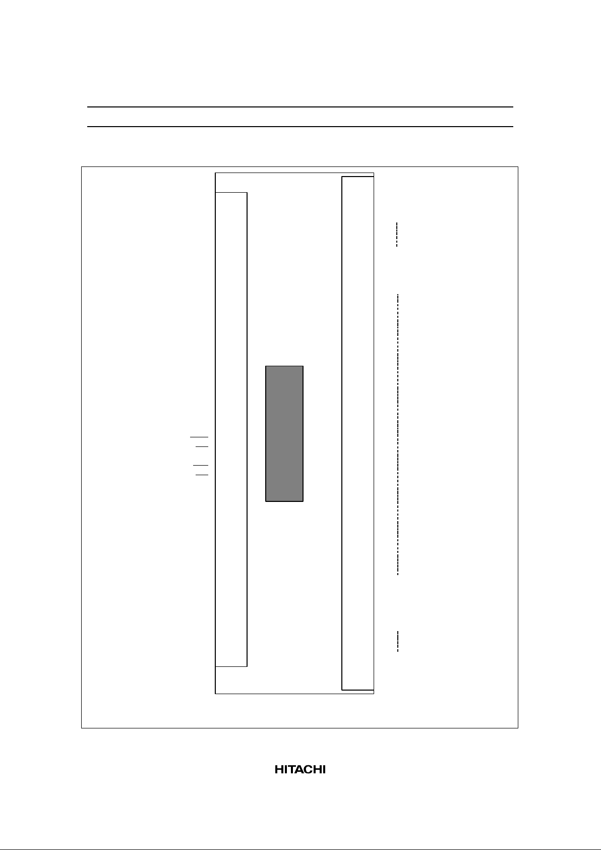
Pin Arrangement
Note: This figure is not drawn to a scale
COM80
COM79
COM78
COM41
SEG160
SEG159
SEG158
COM40
SEG3
SEG2
SEG1
COM39
COM3
COM2
COM1
I/O,Power supply pins
LCD drive signal output pins
GND1
VLCD1
VCC1
V5O
V4O
V3O
V2O
V1O
GREF
IREFM
IREFP
VLCD2
VLCD3
VCC2
GND2
GND3
VCC3
OSC1
OSC2
OSC
CO
DCON
CL1
FLM
M
M/S
RES
CS
RS
WR
RD
VCC4
GND4
DB0
DB1
DB2
DB3
DB4
DB5
DB6
DB7
VCC5
GND5
VCC6
VLCD4
GND6
Page 4

HD66420
4
Pin Description
Pin Name
Number of
Pins I/O Connected to Description
V
CC
1–6,
GND1–6
12 — Power supply VCC: +2.2V to +5.5V, GND: 0V
VLCD1–4 4 — Power supply Power supply to LCD driving circuit
V1O, V2O,
V3O, V4O,
V5O
5 — V1 to V5 of
HD66420
Several levels of power to the LCD driving outputs.
Master HD66420 outputs these levels to the slave
HD66420.
OSC 1 I Oscillator
resister or
Must be connected to external resister when using R-C
oscillation. When using an external clock, it must be
OSC1,
OSC2
2 I/O
external clock input to the OSC terminal.
CO 1 O OSC of Slave
HD66420
Clock output
DCON 1 O External DC/DC
convertor
Controls on/off switch of external DC/DC convertor
CL1 1 I/O CL1 of
HD66420
Line clock
FLM 1 I/O FLM of
HD66420
Frame signal
M 1 I/O M of HD66420 Converts LCD driving outputs to AC
M/S 1 I VCC or GND Specifies master/slave mode.
RES 1 I — Reset the LSI internally when drive low.
CS 1 I MPU Select the LSI, specifically internal registers (index and
data registers) when driven low.
RS 1 I MPU Select one of the internal registers; select the index
register when driven low and data registers when driven
low.
WR 1 I MPU Inputs write strobe; allows a write access when driven
low.
RD 1 I MPU Inputs read strobe; allows a read access when driven
low.
DB7 to DB0 8 I/O MPU 8-bits three-state bidirectional data bus; transfer data
between the HD66420 and MPU through this bus.
SEG1 to
SEG160
160 O LCD Output column drive signals
COM1 to
COM80
80 O LCD Output row drive signals
IREFP 1 — V
CC
Power supply for internal operation amplifier
IREFM 1 — External resistor Bias current for internal operational amplifier
GREF 1 — GND Power supply for internal operation amplifier
Page 5

HD66420
5
Resister List
Index
Reg.Bits Data bits
CS RS 4 3 2 1 0 Register Name R/W 7 6 5 4 3 2 1 0
1 – ––––– –
0 0 – – – – – IR Index register W IR4 IR3 IR2 IR1 IR0
0 1 0 0 0 0 0 R0 Control register 1 W RMW DISP STBY PWR AMP REV HOLT ADC
0 1 0 0 0 0 1 R1 Control register 2 W BIS1 BIS0 WLS GRAY DTY1 DTY0 INC BLK
0 1 0 0 0 1 0 R2 X address register W XA5 XA4 XA3 XA2 XA1 XA0
0 1 0 0 0 1 1 R3 Y address register W YA6 YA5 YA4 YA3 YA2 YA1 YA0
0 1 0 0 1 0 0 R4 Display RAM access register R/W D7 D6 D5 D4 D3 D2 D1 D0
0 1 0 0 1 0 1 R5 Display start line register W ST6 ST5 ST4 ST3 ST2 ST1 ST0
0 1 0 0 1 1 0 R6 Blink start line register W BSL6 BSL5 BSL4 BSL3 BSL2 BSL1 BSL0
0 1 0 0 1 1 1 R7 Blink end line register W BEL6 BEL5 BEL4 BEL3 BEL2 BEL1 BEL0
0 1 0 1 0 0 0 R8 Blink register 1 W BK0 BK1 BK2 BK3 BK4 BK5 BK6 BK7
0 1 0 1 0 0 1 R9 Blink register 2 W BK8 BK9 BK10 BK11 BK12 BK13 BK14 BK15
0 1 0 1 0 1 0 R10 Blink register 3 W BK16 BK17 BK8 BK9
0 1 0 1 0 1 1 R11 Partial display block register W PB3 PB2 PB1 PB0
0 1 0 1 1 0 0 R12 Gray scale palette 1 (0, 0) W GP14 GP13 GP12 GP11 GP10
0 1 0 1 1 0 1 R13 Gray scale palette 2 (0, 1) W GP24 GP23 GP22 GP21 GP20
0 1 0 1 1 1 0 R14 Gray scale palette 3 (1, 0) W GP34 GP33 GP32 GP31 GP30
0 1 0 1 1 1 1 R15 Gray scale palette 4 (1, 1) W GP44 GP43 GP42 GP41 GP40
0 1 1 0 0 0 0 R16 Contrast control register W CM1 CM0 CC4 CC3 CC2 CC1 CC0
0 1 1 0 0 0 1 R17 Reserved –
0 1 1 0 0 1 0 R18 Reserved –
0 1 1 0 0 1 1 R19 Reserved –
0 1 1 0 1 0 0 R20 Reserved –
0 1 1 0 1 0 1 R21 Reserved –
0 1 1 0 1 1 0 R22 Reserved –
0 1 1 0 1 1 1 R23 Reserved –
0 1 1 1 0 0 0 R24 Reserved –
0 1 1 1 0 0 1 R25 Reserved –
0 1 1 1 0 1 0 R26 Reserved –
0 1 1 1 0 1 1 R27 Reserved –
0 1 1 1 1 0 0 R28 Reserved –
0 1 1 1 1 0 1 R29 Reserved –
0 1 1 1 1 1 0 R30 Reserved –
0 1 1 1 1 1 1 R31 Reserved –
Page 6

HD66420
6
RMW
RMW = 1: Read-modify-write mode; Address is incremented only after write access
RMW = 0: Address is incremented after both write and read access
DISP
DISP = 1: Display on
DISP = 0: Display off
STBY
STBY = 1:Internal operation and power circuit halt; display off
STBY = 0: Normal operation
PWR
PWR = 1: Output ‘High’ from DCON
PWR = 0: Output ‘Low’ from DCON
AMP
AMP = 1: OP amp enable
AMP = 0: OP amp disable
REV
REV = 1: Reverse display
REV = 0: Normal display
HOLT
HOLT = 1: Internal operation stops, Oscillator works
HOLT = 0: Internal operation starts
ADC
ADC = 1: Data in X address H’0 is output from SEG160
ADC = 0: Data in X address H’0 is output from SEG1
BIS1, 0
BIS1, 0 = (1,1): 1/6 LCD drive levels bias ratio
BIS1, 0 = (1,0): 1/7 LCD drive levels bias ratio
BIS1, 0 = (0,1): 1/8 LCD drive levels bias ratio
BIS1, 0 = (0,0): 1/9 LCD drive levels bias ratio
WLS
WLS = 1: 6-bit data is valid
WLS = 0: 8-bit data is valid
GRAY
GRAY = 1: Grayscale palette is available(gray scales can be selected from 32-levels)
GRAY = 0: Grayscale palette is not available(4-gray scales fixed)
Page 7

HD66420
7
DTY1, 0
DTY1, 0 = (1,1): 1/8 display duty cycle - Partial display
DTY1, 0 = (1,0): 1/32 display duty cycle
DTY1, 0 = (0,1): 1/64 display duty cycle
DTY1, 0 = (0,0): 1/80 display duty cycle
INC
INC = 1: X address is incremented for each access
INC = 0: Y address is incremented for each access
BLK
BLK = 1: Blink function is used
BLK = 0: Blink function is not used
Page 8

HD66420
8
Block Diagram
RD
WR CS
RS
DB7
-DB0
OSC
RES
OSC2
V3O
V2O
V5O
V4O
VLCD
FLM M CL1
CO
DCON
V1O
OSC1
M/S
Column Driver
Y Decoder
X Decoder
Row
Counter
320 x 80bit
Display memory
Level Shifter
Data Latch2
Data Latch1
COM1 COM40 SEG1 SEG160COM41 COM80
X Address Counter
Start Line Register
Attribute
Comparator
Blink End Line Register
Blink Start Line Register
Control Register
MPU Interface
Display Line
Counter
Row Driver
Oscillator
LCD driver power supply,
Contrast control
Y Address Counter
Data Buffer
Timing
Generator
Grey scale selector
Grey scale
palette
320
160
Level Shifter
Grey
scale
pattern
Generator
Contrast Control Register
Decoder
320
320
Row Driver
Level Shifter
I/O control
Blink Registers
MPX
Page 9

HD66420
9
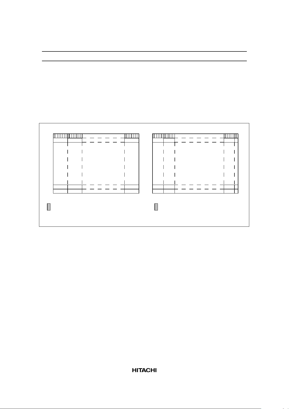
System Description
The HD66420 can display a maximum of 160 × 80 dots (ten 16x16-dot characters × 5 lines) four-level gray
scale or four colour LCD panel. Four levels of gray scale can be selected from 32-levels, so the appropriate
4-level gray scale can be displayed.
The HD66420 can reduce power dissipation without affecting display because data is retained in the
display RAM even during standby modes. An LCD system can be configured simply by attaching external
power supply, capacitors and resistors (figure 1) since the HD66420 incorporates power circuits.
COM1 to
COM40
HD66420
LCD panel
MPU
8
SEG1 to
SEG160
CS
RS
RD
WR
DB7 to DB0
COM41 to
COM80
DC/DC
Convertor
Figure 1 System Block Diagram
Page 10

HD66420
10
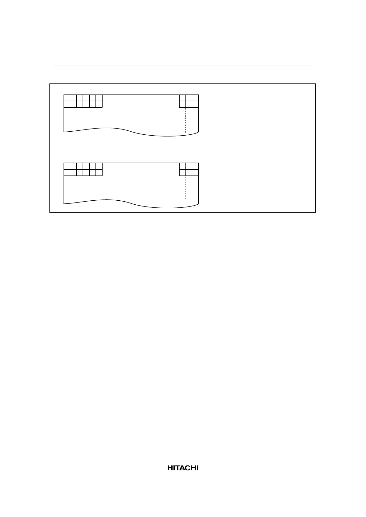
MPU Interface
The HD66420 can interface directly to an MPU through an 8-bit data bus or through an I/O port (figure 2).
The MPU can access the HD66420 internal registers independently of internal clock timing.
The index register can be directly accessed but the other registers (data registers) cannot. Before accessing
a data register, its register number must be written to the index register. Once written, the register number is
held until it is rewritten, enabling the same register to be consecutively accessed without having to rewrite
to the register number for each access. An example of a register access sequence is shown in figure 3.
C0
C1
C2
C3
A0 - A7
CS
RS
RD
WR
DB0 - DB7
H8/325 HD66420
8
a) Interface through Bus
A15 - A0
A0
RD
WR
D0 - D7
CS
RS
RD
WR
DB0 - DB7
Z80 HD66420
8
b) Interface through I/O Port
decoder
Figure 2 8-Bit MPU Interface Examples
Page 11

HD66420
11
RD
WR
DB7 to
DB0
Write index
register
RS
CS
Write data
register
Write index
register
Read data
register
Read data
register
Data
Data Data Data Data Data
Write data
register
Figure 3 8-Bit Data Transfer Sequence
Page 12

HD66420
12
LCD Driver Configuration
Row and column outputs: The HD66420 outputs row signals from both sides. In any case, each output’s
function is fixed; COM1 to COM80 output row signals and SEG1 to SEG160 output column signals.
Dot-matrix Display
40-channel
row output
160-channel column
output
40-channel
row output
Row outputs from
both sides of LCD
160 × 80
HD66420
COM41 to
COM80
COM1 to
COM40
SEG1 to SEG160
Figure 4 Common outputs from both sides
Page 13

HD66420
13
Column Address Inversion According to LCD Driver Layout: The HD6420 can always display data in
address H’0 on the top left of an LCD panel regardless of where it is positioned with respect to the panel.
This is because the HD66420 can invert the positional relationship between display RAM addresses and
LCD driver output pins by inverting RAM addresses. Specifically, the HD66420 outputs data in address
H’0 from SEG1 when the ADC bit in control register 1 is 0, and from SEG160 otherwise. Here, the scan
direction of row output is also inverted according to the situation as shown in figure 6. Note that addresses
and scan direction are inverted when data is written to the display RAM, and thus changing the ADC bit
after data has been written has no effect. Therefore. hardware control bits such as ADC must be set
immediately after reset is canceled, and must not be set while data is being displayed.
COM1
COM40LCD panel
COM80
COM41
b) ADC = 1
SEG1
SEG2
SEG3
SEG158
SEG159
SEG160
SEG157
SEG156
SEG155
SEG154
SEG153
COM80
COM41
COM1
COM40
a) ADC = 0
H’0
SEG1
SEG2
SEG3
SEG4
SEG5
SEG6
SEG7
SEG8
SEG158
SEG159
SEG160
LCD panel
H’1
HD66420
HD66420
H’0 H’1
Figure 5 LCD Driver Layout and RAM addresses : 1/80 Duty cycle
Table 1 Scanning Direction and RAM Address
DTY1 DTY0 ADC COMMON SEGMENT
0 0 0 COM1 → COM40, COM80 → COM41 H’00 → SEG1
1 COM41 → COM80, COM40 → COM1 H’00 → SEG160
1 0 COM1 → COM32, COM80 → COM49 H’00 → SEG1
1 COM49 → COM80, COM32 → COM1 H’00 → SEG160
1 0 0 COM1 → COM16, COM80 → COM65 H’00 → SEG1
1 COM65 → COM80, COM16 → COM1 H’00 → SEG160
1 0 8 COM depend on R11 H’00 → SEG1
1 8 COM depend on R11 H’00 → SEG160
Page 14

HD66420
14
Multi-LSI Operation
Using multiple HD66420s provides the means for extending the number of display dots. Note the following
items when using the multi-LSI operation.
(1) The master LSI and the slave LSI must be determined; the M/S pin of the master LSI must be set high
and the M/S pin of the slave LSI must be set low.
(2) The master LSI supplies the FLM, M, CL1 and clock signals to the slave LSI via the corresponding
pins, which synchronizes the slave LSI with the master LSI.
(3) All control bits of slave LSI must be set with the same data with that of the master LSI.
(4) All LSIs must be set to LCD off in order to turn off the display.
(5) The standby function of slave LSI must be started up first, and that of the master LSI must be
terminated first.
(6) The power supply circuit of slave LSI stop working, so V1 to V5 levels are supplied from the master
LSI. If the internal power supply circuit can not drive two LSIs, use an external power supply circuit.
Figure 6 shows the configuration using two HD66420s and table 2 lists the differences between master and
slave modes.
Dot-matrix Display
40-channel
row output
160-channel
column output
40-channel
row output
320 x 80
HD66420
(Master)
160-channel
column output
HD66420
(slave)
CL1FLMM CL1FLMM OSCCOOSC OSC1 CO OSC1
Open
V1O to
V5O
V1O to
V5O
Figure 6 Configuration Using Two HD66420s
Page 15
HD66420
15
Table 2 Comparison between Master and Slave Modes
Item Master Mode Slave Mode
Pin M/S Must be set high Must be set low
OSC Oscillation is active Oscillation is active
CO Output High-Z
FLM, M, CL1 Output signals Input signals
Registers R0, R2 to R15 Valid Valid
R1: BIS1, 0 Valid Invalid
R1: other Valid Valid
R16 Valid Invalid
Power supply circuit Valid Invalid
Page 16

HD66420
16
Display RAM Configuration and Display
The HD66420 incorporates a bit-mapped display RAM. It has 320 bits in the X direction and 80 bits in the
Y direction. The 320 bits are divided into forty 8-bit groups. As shown in figure 6, data written by the MPU
is stored horizontally with the MSB at the far left and the LSB at the far right. The consecutive two bits
control one pixel of LCD, this means that one 8-bits data contains data which controls four pixels.
The ADC bit of control register 1 can control the positional relationship between X addresses of the RAM
and LCD driver output (figure 7). Specifically. the data in address H’0 is output from SEG1 when the ADC
bit in control register 1 is 0, and from SEG160 otherwise. Here, data in each 8-bit group is also inverted.
Because of this function, the data in X address H’0 can be always displayed on the top left of an LCD panel
with the MSB at the far left regardless of the LSI is positioned with respect to the panel. In this case, DB7,
DB5, DB3 and DB1 are more significant bit in consecutive two bits.
SEG1
SEG2
SEG3
SEG4
11100100
00011011
Y0
Y1
D
B
7
D
B
1
LCD panel
Display RAM
SEG157
SEG158
DEG159
SEG160
11100100
00011011
Y0
Y1
D
B
7
D
B
0
LCD panel
Display RAM
D
B
6
D
B
4
D
B
5
D
B
2
D
B
3
D
B
1
D
B
6
D
B
5
D
B
4
D
B
3
D
B
2
D
B
0
(a) ADC = 0 (b) ADC = 1
SEG160 SEG1
Figure 7 Display RAM Data and Display
Page 17

HD66420
17
H’00
H’01
H’0 H’1
H’27
X addresses
SEG1
SEG160
LCD drive signal output
(a) ADC = 0
(b) ADC = 1
H’4E
H’4F
H’00
H’01
H’0
H’26
H’27
SEG1
SEG160
H’4E
H’4F
Y address
MSB MSB
LCD drive signal output
Y address
X addresses
Figure 8 Display RAM Configuration
Page 18
HD66420
18
Word Length
The HD66420 can handle either 8- or 6-bits as a word. In the display memory, one X address is assigned to
each word of 8- or 6-bits long in X direction.
When the 6-bits mode is selected, only data on DB5 to DB0 are used and data on DB7 and DB6 are
discarded. This word length is only applied to data to internal RAM. The word length of internal register is
always 8-bits
H’00
H’01
H’0 H’1
H’27
X addresses
SEG1
SEG160
LCD drive signal output
(a) Address assignment when one
word is 8 bits long
H’4E
H’4F
H’00
H’01
H’35
H’1
H’0
SEG1
SEG160
H’4E
H’4F
Y address
MSB MSB
LCD drive signal output
Y address
X addresses
H’34
(b) Address assignment when one
word is 6 bits long
8 bits 6 bits
Figure 9 Display RAM Addresses
Page 19
HD66420
19
111001
000110
Y0
Y1
D
B
1
Display RAM
100
011
D
B
1
D
B
0
D
B
4
D
B
0
D
B
3
D
B
2
D
B
5
D
B
4
(a) WLS= 1, ADC = 0
H’35’s bit7,6, and 3 to 0 are disable .
(b) WLS= 1, ADC = 1
H’0’s bit7 to 2 are disable.
111001
000110
Y0
Y1
D
B
5
Display RAM
100
011
D
B
5
D
B
4
D
B
0
D
B
4
D
B
3
D
B
2
D
B
1
D
B
0
H’0H’35
H’35H’0
Figure 10 Display RAM Bits Map
Page 20

HD66420
20
Configuration of Display Data Bit
Packed Pixel Method
For grey scale display and super reflective colour display, multiple bits are needed for one pixel. In the
HD66420, two bits are assigned to one pixel, enabling a four-level grey scale display and four colour
display.
One address, eight bits, specifies four pixels, and pixel bits 0 and 1 for gray scale are managed as
consecutive bits in one byte.
When grey scale display data is manipulated in bit units, one memory access is sufficient, which enables
smooth high-speed data rewriting.
The bit data to input to pin DB7, DB5, DB3 and DB1 become MSB and the bit data to input via pin DB6,
DB4, DB2 and DB0 are LSB.
00011011
76543210Bit
FRC control circuit
Grey scale/colour palette
Physical memory
LCD display state
00001010
76543210
4 pixels/address
Address: n
Address: n + 1
Figure 11 Packed Pixel Method
Page 21

HD66420
21
Gray scale/Colour palette
The HD66420 uses PWM, Pulse Width Modulation, technique for gray scale display. A period of one line
is divided into thirty-one or four and HD66420 outputs turn-on levels for one period and turn-off levels for
rest of these period. This technique changes gray scale on monochrome display and colour on super
reflective colour panel. The characteristics of these panel vary with different panel. To allow for this, the
HD66420 designed to generate 32-levels gray scale levels and provides palette registers that assign desired
levels to certain of the four colours, GRAY = 0, or generate dedicated 4-level grayscale , GRAY = 1. Using
the palette registers to select any 4 out of 32 levels of applied voltages enables an optimal grayscale/colour
display. Because of this grayscale technique using 32-levels gray scale needs higher clock rate. If 32-levels
gray scale is not needed, lower clock rate can be used. Table 3 shows default value of palette registers and
Table 4 and 5 show relationship between value of a palette register and grayscale level.
Table 3 Default Value of Palette Registers
DB7, 5, 3, 1 DB6, 4, 2, 0 Register Name Default Value
0 0 Grayscale Palette 1 0 0 0 0 0
1 Grayscale Palette 2 0 1 0 1 1
1 0 Grayscale Palette 3 1 0 1 1 1
1 Grayscale Palette 4 1 1 1 1 1
Page 22
HD66420
22
Table 4 Value of a Palette Register and Grayscale Levels (GRAY= 0)
Value Grayscale Level
0 0 0 0 0 0 defaust R12
1 1/31
1 0 2/31
1 3/31
1 0 0 4/31
1 5/31
1 0 6/31
1 7/31
1 0 0 0 8/31
1 9/31
1 0 10/31
1 11/31 defaust R13
1 0 0 12/31
1 13/31
1 0 14/31
1 15/31
1 0 0 0 0 16/31
1 17/31
1 0 18/31
1 19/31
1 0 0 20/31
1 21/31
1 0 22/31
1 23/31 defaust R14
1 0 0 0 24/31
1 25/31
1 0 26/31
1 27/31
1 0 0 28/31
1 29/31
1 0 30/31
1 1 defaust R15
Page 23

HD66420
23
Table 5 Grayscale Levels (GRAY= 1)
DB7, 5, 3, 1 DB6, 4, 2, 0 Grayscale Level
00 0
1 1/3
1 0 2/3
11
Access to Internal Registers and Display RAM
Access to Internal Registers by the MPU: The internal registers include the index register and data
registers. The index register can be accessed by driving both the CS and RS signals low. To access a data
register, first write its register number ID to the index register with RS set to 0, and then access the data
register with RS set to 1 . Once written, the register number is held until it is rewritten, enabling the same
register to be consecutively accessed without having to rewrite to the register number for each access.
Some data registers contain unused bits; they should be set to 0. Note that all data registers except the
display memory access register can only be written to.
Access to Display RAM by the MPU: To access the display RAM, first write the RAM address desired to
the X address register (R2) and the Y address register (R3). Then read/write the display memory access
register (R4). Memory access by the MPU is independent of memory read by the HD66420 and is also
asynchronous with the HD66420’s clock, thus enabling an interface independent of HD66420’s internal
operations.
However, when reading. data is temporarily latched into a H66420’s buffer and then output next time, a
read is performed in a subsequent cycle. This means that a dummy read is necessary after setting X and Y
addresses. The memory read sequence is shown in figure 12.
X and Y addresses are automatically incremented after each memory access according to the INC bit value
in control register 2; therefore, it is not necessary to update the addresses for each access. Figure 13 shows
two cases of incrementing display RAM address. When the INC bit is 0, the Y address will be incremented
up to H’7F with the X address unchanged. However, actual memory is valid only within H’00_ to H’4F;
accessing an invalid address is ignored. When the INC bit is 1 , the X address will be incremented up to
H’27 or H’35 according to WLS bit with the Y address unchanged. After address H’27 or H’35, the X
address will be returned to H’00; accessing more than forty bytes causes rewriting to the same address.
Page 24

HD66420
24
[n] [m]
Data[n,m] Data[n,m+1]
Undetermined
H’02 H’03 H’04
WR
Input
data
Output
data
Dummy
read
[n,*] [n,m]
[n,m+1] [n,m+2]
[*,*]Address
RS
RD
X Address Y Address
Figure 12 Display RAM read sequence
Page 25

HD66420
25
Display RAM Reading by LCD Controller:
Data is read by the HD66420 to be displayed asynchronously with accesses by the MPU. However, because
simultaneous access could damage data in the display RAM, the HD66420 internally arbitrates access
timing; access by the MPU usually has priority and so access by the HD66420 is placed between accesses
by the MPU. Accordingly, an appropriate time must be secured (see the given electrical characteristics
between two accesses by the MPU).
a) INC = 0
H’0
H’1 H’27
H’00
H’01
H’7F
H’28 H’35
WLS= 0
WLS= 1
b) INC = 1
H’0 H’1 H’27
H’00
H’01
H’02
H’4F
H’28 H’35
WLS= 0
WLS= 1
WLS= 0
WLS= 1
H’4F
Valid area
Invalid area
Valid area (WLS= 1)
Invalid area
Figure 13 Display Address Increment
Page 26

HD66420
26
Read-Modify-Write: X- or Y-address is incremented after reading form or writing data to the display
RAM at normal mode. However, X- or Y-address is not incremented after reading data from the display
RAM at read-modify-write mode. The data which is read from the display RAM may be modified and
written to the same address without re-setting the address. Data is temporarily latched into a HD66420’s
buffer and then output next time a read is performed in a subsequent cycle. This means that the dummy
read is necessary after every cycle. This sequence is shown in figure 14.
Set X-address
Set Y-address
dummy read
Read Data
Write Data
Finish Modifying
no
yes
Address
incremented
START
END
Figure 14 The Flow Chart for Read-Modify-Write
Page 27

HD66420
27
Vertical Scroll Function
The HD66420 can vertically scroll a display by varying the top raster to be displayed. which is specified by
the display start raster register. Figure 15 and 16 show vertical scroll examples. As shown, when the top
raster to be displayed is set to l, data in Y address H’00_ is displayed on the 80th raster. To display another
frame on the 80th raster, therefore, data in Y address H’00_ must be modified after setting the top raster.
When display duty is less than 80, for example 1/64, data of address H’40 is displayed after address H’3F.
Page 28

HD66420
28
H’00
H’01
H’02
H’03
H’04
H’05
H’06
H’07
H’08
H’09
H’0A
H’4C
H’4D
H’4E
H’4F
Y-address
Top raster to be
displayed = 0
Top raster to be
displayed = 2
Y-address
H’00
H’01
H’4E
H’4F
H’0B
H’0C
H’02
H’03
H’04
H’05
H’06
H’07
H’08
H’09
H’0A
Y-address
Top raster to be
displayed = 1
H’0B
H’01
H’02
H’03
H’04
H’05
H’06
H’07
H’08
H’09
H’0A
H’00
H’4D
H’4E
H’4F
Figure 15 Vertical Scroll : 1/80Duty Cycle
Page 29

HD66420
29
Y-address
Y-address
Top raster to be
displayed = 0
Top raster to be
displayed = 1
Top raster to be
displayed = 2
Y-address
H’00
H’01
H’02
H’03
H’04
H’05
H’06
H’07
H’08
H’09
H’0A
H’3C
H’3D
H’3E
H’3F
H’0B
H’01
H’02
H’03
H’04
H’05
H’06
H’07
H’08
H’09
H’0A
H’40
H’3D
H’3E
H’3F
H’0C
H’02
H’03
H’04
H’05
H’06
H’07
H’08
H’09
H’0A
H’3E
H’3F
H’41
H’0B
H’40
Figure 16 Vertical Scroll : 1/64Duty Cycle
Page 30

HD66420
30
Partial Display Function
The HD66420 can display only a part of a full display. The bias ratio of this partial display is 1/4 from V
CC
to GND, the duty ratio is 1/8 and rest of display is scanned with unselected levels. 8 levels of contrast can
be selected wit data bit 2 to 0 of R16. The position of this partial display can be located at any position with
using partial display position register. To launch this mode, following processes are needed:
(1) supplied voltage to VLCD must be cut off, PWR bit can be used if external voltage supplier is
controlled with DCON output (R0)
(2) set DTY0, 1 bits (R1)
(3) set COM scanning direction (ADC bit)
(4) set display position (R11, R5)
(5) set contrast level (R16 data-bit 2 to 0)
The clock frequency may be 180kHz at normal display mode. When a partial display is driven, oscillation
frequency will be 18kHz, 1/10 of that of normal display mode. This function is useful for lower power
dissipation. To change clock frequency, follow the process which is showed in Figure 21.
Warning: VLCD must be cut off when partial display mode is launched. Vcc is supplied to LCD
driving circuit instead of VLCD. So if VLCD is supplied externally during partial display mode, Vcc
short-circuit to VLCD.
Table 6 Partial Display Block
R11 ADC = 1 ADC = 0
H’00 COM1 → COM8 COM8 → COM1
H’01 COM9 → COM16 COM16 → COM9
H’02 COM17 → COM24 COM24 → COM17
H’03 COM25 → COM32 COM32 → COM25
H’04 COM33 → COM40 COM40 → COM33
H’05 COM80 → COM73 COM73 → COM80
H’06 COM72 → COM65 COM65 → COM72
H’07 COM64 → COM57 COM57 → COM64
H’08 COM56 → COM49 COM49 → COM56
H’09 COM48 → COM41 COM41 → COM48
Page 31

HD66420
31
Display
RAM
Y address
H’00
LCD panel
COM1
COM33
COM40
COM80
COM41
H’4F
R5
Start line
R5+7
R11 = H’04
ABCD
ABCD
Figure 17 Partial Display
Page 32

HD66420
32
Blink Function
The HD66420 can blink a specified area on the dot-matrix display. Blinking is achieved by repeatedly
turning on and off the specified area at a frequency of one sixty-fourth the frame frequency. For example,
when the frame frequency is 80 Hz. the area is turned on and off every 0.8 seconds.
The area to be blinked can be designated by specifying vertical and horizontal positions of the area. The
vertical position or the rasters to be blinked, are specified by the blink start raster register (R6) and blink
end raster register (R7).
The horizontal position, or the dots to be blinked in the specified rasters, are specified by the blink registers
R8, R9 and R10 in an 8-dot group; each data bit in the blink registers controls its corresponding 8-dots
group. The relationship between the registers and blink area is shown in figure 18. Setting the BLK bit to 1
in control register 2 after setting the above registers starts blinking the designated area. Note that since the
area to be blinked is designated absolutely with respect to the display RAM, it will move along with a
scrolling display (figure 19).
0000001111100001
D
B
7
D
B
6
D
B
5
D
B
4
D
B
3
D
B
2
D
B
1
D
B
0
D
B
7
D
B
6
D
B
5
D
B
4
D
B
3
D
B
2
D
B
1
D
B
0
Blink start
line (R6)
Blink end
line (R7)
Blink registers
R8 R9
Blink area
SEG1
LCD
SEG9
SEG17
SEG25
SEG33
SEG41
SEG49
SEG57
SEG65
SEG73
SEG81
SEG89
SEG97
SEG105
SEG113
SEG121
SEG129
SEG137
SEG145
SEG153
0001
SEG160
D
B
3
D
B
2
D
B
1
D
B
0
R10
Figure 18 Blink Area Designation by Blink Control Registers
Page 33

HD66420
33
Display start raster = 0
Blink start raster = 0
Blink end raster = H’F
Display start raster = H’5
Blink start raster = H’5
Blink end raster = H’F
Figure 19 Scrolling Blink Area
Page 34
HD66420
34
Power Down Modes
The HD66420 has a standby function providing low power-dissipation, which is initiated by internal
register settings. During standby mode, all the HD66420 functions are inactive and data in the display
RAM and internal registers except the DISP bit are retained. However, only control registers can be
accessed during standby mode. HD66420 has an another power down mode: partial display. In this mode
only a part of display is active. However, this duty ratio is 1/8 so the external power supply for LCD drive
will be inactive. The oscillator does not halt, thus dissipating more power than standby mode. Table 7 lists
the LCD driver output pin status during standby mode. Figure 20 shows the procedure for initiating and
canceling a standby mode and figure 21 shows the procedure for changing oscillator. Note that these
procedure must be strictly followed to protect data in the display RAM.
Table 7 Output Pin Status during Power Down modes
Signal Name STBY Status
COM1–COM80 1 Output VLCD (display off)
0 Output common signals (VLCD–GND)
SEG1–SEG160 1 Output VLCD (display off)
0 Output segment signals (VLCD–GND)
Set STBY bit to 1 (control register 1)
Clear STBY and PWR bits to 0 (control register 1)
Oscillation halts
External power supply off
Oscillator starts
Internal operation starts
Display starts
Standby mode
Initiation
Cancellation
Wait for oscillation and external
power supply to stabilize
Set DISP bit to 1 (control register 1)
Figure 20 Procedure for Initiation and Canceling a Standby Mode
Page 35

HD66420
35
Set HOLT bit to 1 (control register 1)
Set DTY or GRAY bit to 1 (control register 2)
Internal operation stops
Oscillator 2 starts working
Wait for oscillation to stabilize
Clear HOLT bit to 0 (control register 1)
Internal operation starts
Figure 21 Procedure for Changing Oscillator
Page 36

HD66420
36
Power On/Off Procedure
Figure 22 shows the procedure for turning the power supply on and off. This procedure must be strictly
followed to prevent incorrect display because the HD66420 incorporates a power supply circuit.
Boosting starts
Power on
Turn on power (power-on reset)
Set PWR bit to 1 (control register 1)
Write data to registers and RAM as required
Set DISP bit to 1 (control register 1)
Set CNF, ADC, DTY1, DTY0, INC bits according to
the operating mode (control register1 and 2)
Turn off power
Clear DISP bit to 0 (control register 1)
Power off
Boosting halts
Clear PWR bit to 0 (control register 1)
Figure 22 Procedure for Turning Power Supply On/Off
Page 37

HD66420
37
Oscillator
The HD66420 incorporates two sets of R-C oscillator for two display modes: OSC-OSC1 oscillator is used
for 32-levels gray scale display mode and OSC-OSC2 oscillator for 4-levels gray scale display mode. If the
internal oscillator is not used, an appropriate clock signal must be externally input through the OSC pin. In
this case, the OSC1 and OSC2 pins must be left unconnected. Oscillation resister must be placed near LSI,
because if capacitance exists between OSC and OSC1 oscillator may not work properly. Figure 23 shows
oscillator connections.
Changing Oscillator
Two oscillators are alternated automatically depending on modes. The resistor between OSC and OSC1 is
used during 32-levels grayscale mode and the resistor between OSC and OSC2 is used during 4-levels
grayscale mode. An external clock must be input from OSC terminal at any modes.
Clock and Frame Frequency
The HD66420 generates the frame frequency by dividing the input clock. Clock frequency is determined
with following equation:
f
OSC
= N * (Duty ratio) * (Frame frequency)
N: 31 for 32-level gray scale display mode
3 for 4-level gray scale display mode
The frame frequency is usually 70 to 90 Hz; when the frame frequency is 70 Hz, for example, the input
clock frequency will be 180 kHz for 32-level gray scale display mode, and 18kHz for 4-level gray scale.
OSC
OSC2
Clock
(Open)
OSC
OSC1
HD66420
HD66420
a) External clock b) Dual oscillator
Rf1
OSC1
(Open)
OSC2
OSC
OSC1
HD66420
c)Single oscillator
Rf
OSC2
(Open)
Rf2
Figure 23 Oscillator Connections
Page 38

HD66420
38
Power Supply Circuits
HD66420 has following circuits for power supply circuit: operational amplifiers, resistive dividers, bias
control circuit and contrast control circuit. LCD driving voltage, VLCD, must be generated externally.
LCD Drive Voltage Power Supply Levels: To drive the LCD, a 6-level power supply is necessary. These
levels are generated internally or supplied from outside. When an internal voltage levels generator is
chosen, external capacitors are needed to stabilize these levels. AS the HD66420 incorporates operational
amplifiers to these levels, this circuit gives better quality of display with less power consumption. This
divided ratio is programmable.
Bias current of internal operational amplifier is determined with a resister which is inserted between
IREFM and GND. This resister value is between 1MΩ and 5MΩ. Larger resister value make less power
consumption at internal operational amplifier. However, too large value loose operational margin of
amplifiers.
Keep following relationship among voltage levels;
VCC ≥ IREFMP > IREFM ≥ GND
VLCD > VCC > GREF ≥ GND
VLCD ≥ V1O ≥ V2O ≥ V3O ≥ V4O ≥ V5O ≥ GREF
VLCD–VCC ≥ 1.0V
IREFP–IREFM ≥ 1.0V
VCC–GREF ≥ 1.0V
Contrast Control: Internal contrast control circuit can change the output voltage level of VLCD by setting
data to contrast control register, R16. VLCD adjustable range are showed below;
• 1/6 bias
0.75 * (VLCD-GND) ≤ VLCD ≤ 0.99 * (VLCD-GND)
• 1/9 bias
0.82 * (VLCD-GND) ≤ VLCD ≤ 0.993 * (VLCD-GND)
Page 39

HD66420
39
0
V5O
V4O
V3O
V2O
V1O
VLCD
Example.1 LCD bias level
1/80 duty Display (1/9 bias, VLCD = 12V, GND = 0V)
Voltage [V]
0
1
2
3
4
5
6
7
8
9
10
11
12
07 0F
Contrast (R16)
17 1F
(maximum)
0
V5O
V4O
V3O
V2O
V1O
V
CC
Example.2 LCD bias level
Partial Display (1/4 bias, VCC = 5V, GND = 0V)
Voltage [V]
0
1
2
3
4
5
4
Contrast (R16)
7
(maximum)
• Partial display
0.82 * (VCC-GND) ≤ VCC ≤ 0.997 (VCC-GND)
Partial display function uses 1/4 bias ratio from VCC to GND. Eight levels of contrast can be selected
with data bit 2 to 0 of R16.
LCD drive levels bias ratio: LCD driving levels bias ratio can be selected from 1/6, 1/7, 1/8 or 1/9.
Power Supply: The HD66420 needs the external power supply for LCD driving circuit. If this power
circuit has on/off control, the HD66420 controls the external power supply circuit by setting PWR bit.
External Power Supply Circuit: When the internal operational amplifier cannot fully drive the LCD panel
used, V1O to V5O voltages can be supplied from external power supply circuit. Here, the AMP bit must be
set to 1 to turn off the internal power supply circuit.
Page 40

HD66420
40
-
+
-
+
-
+
-
+
V2O
V3O
V4O
V5O
IV1
IV2
IV3
IV4
GREF
R1
R1
R3
R1
R1
VLCD
R2
Contrast
control
circuit
Bias
control
V1O
HD66420
DCON
External voltage
booster
on/off
Vout
-
+
IV5
R4
IREFP
IREFM
GND
Vcc
VLCD
Operational
amplifier OFF
resistive divider for
partial display mode
r
r
r
r
R1 = R
R2 = 0.0625R to 2R
R3 = 2R to 5R
R4 = 1MΩ to 5MΩ
C1 = 1µF to 3µF
Resister for
bias current
of operational
amplifier
C1
C1
C1
C1
C1
Figure 24 Power Supply Circuit
Page 41

HD66420
41
Reset
The low RES signal initializes the HD66420, clearing all the bits in the internal registers. During reset. the
internal registers cannot be accessed.
Note that if the reset conditions specified in the Electric Characteristics section are not satisfied, the
HD66420 will not be correctly initialized. In this case, the internal registers of the HD66420 must be
initialized by software.
Initial Setting of Internal Registers: All the internal register bits are cleared to 0. Details are listed below.
Normal operation
Oscillator is active; OSC-OSC1 is used
Display is off
Y address of display RAM is incremented
1/80 duty cycle
X and Y addresses are 0
Data in address H’0 is output from the SEGl pin
Blink function is inactive
Operational amplifier is disabled
Initial Setting of Pins:
Bus interface pins
During reset, the bus interface pins do not accept signals to access internal registers; data is undefined when
read.
LCD driver output pins
During reset. all the LCD driver output pins (SEG1 to SEGl61, COM1 to COM80) output Vcc-level
voltage, regardless of data value in the display RAM, turning off the LCD. Here, the output voltage is not
alternated. Note that the same voltage (VLCD) is applied to both column and row output pins to prevent
liquid crystals from degrading.
Internal Registers
The HD66420 has one index register and 17 data registers, all of which can be accessed asynchronously
with the internal clock. All the registers except the display memory access register are write-only.
Accessing unused bits or addresses affects nothing; unused bits should be set to 0 when written to.
Index Register (IR): The index register (figure 25) selects one of 17 data registers. The index register
itself is selected when both the CS and RS signals are low. Data bits 7 to 5 are unused; they should be set to
0 when written to.
Page 42

HD66420
42
Control Register 1 (R0): Control register 1 (figure 26) controls general operations of the HD66420. Each
bit has its own function as described below.
RMW bit
RMW = l: Read-modify-write mode Address is incremented only after write access
RMW = 0: Address is incremented after both write and read accesses
DISP bit
DISP = 1: Display on
DISP = 0: Display off (all LCD driver output pins output VLCD level)
STBY bit
STBY = l: Internal operation and oscillation halt; display off
STBY = 0: Normal operation
PWR bit
PWR = l: Output high level from DCON terminal
PWR = 0: Output low level from DCON terminal
This bit controls the external power supply for LCD driving outputs.
AMP bit
AMP = 1: OP amp enable
AMP = 0: OP amp disable
REV bit
REV = 1: Reverse display
REV = 0: Normal display
HOLT bit
HOLT = l : Internal operation stops
HOLT = 0: Internal operation starts
ADC bit
ADC = l: Data in X address H’0 is output from SEG160; row signals depend on duty.
ADC = 0: Data in X address H’0 is output from SEG1; row signals are scanned from COM1.
Data bit
Set value
76543210
Register number
Figure 25 Index Register (IR)
Page 43

HD66420
43
Data bit
Set value
76543210
RMW DISP STBY PWR AMP REV HOLT ADC
Figure 26 Control Register 1 (R0)
Control Register 2 (R1): Control register 2 (figure 27) controls general operations of the HD66420. Each
bit has its own function as described below.
BIS1, BIS0 bits
BIS1, 0 = (1, 1): 1/6 LCD drive levels bias ratio
BIS1, 0 = (1, 0): 1/7 LCD drive levels bias ratio
BIS1, 0 = (0, 1): 1/8 LCD drive levels bias ratio
BIS1, 0 = (0, 0): 1/9 LCD drive levels bias ratio
WLS bit
WLS = l: A word length is 6-bits
WLS = 0: A word length is 8-bits
GRAY bit
GRAY = l : 4-levels of gray scale are fixed
GRAY = 0: 4-levels of gray scale are selected from 32-levels
DTY1,DTY0 bits
DTY1, 0 = (1, 1): 1/8 display duty cycle; partial display mode
DTY1, 0 = (1, 0): 1/32 display duty cycle
DTY1, 0 = (0, 1): 1/64 display duty cycle
DTY1, 0 = (0, 0): 1/80 display duty cycle
INC bit
I NC = l: X address is incremented for each access
INC = 0: Y address is incremented for each access
BLK bit
BLK = 1: Blink function is used
BLK = 0: Blink function is not used
The blink counter is reset when the BLK bit is set to 0. It starts counting and at the same time initiates
blinking when the BLK bit is set to l.
X Address Register (R2): The X address register (figure 28) designates the X address of the display RAM
to be accessed by the MPU. The set value must range from H’00 to H’27 in the case of 8-bit a word or
range from H’00 to H’35 in the case of 6-bit a word; setting a greater value is ignored. The set address is
automatically incremented each time the display RAM is accessed; it is not necessary to update the address
each time. Data bits 7 and 6 are unused; they should be set to 0 when written to.
Page 44

HD66420
44
Y Address Register (R3): The Y address register (figure 29) designates the Y address of the display RAM
to be accessed by the MPU. The set value must range from H’00 to H’40; setting a greater value is ignored.
The set address is automatically incremented each time the display RAM is accessed; it is not necessary to
update the address each time. Data bit 7 is unused; it should be set to 0 when written to.
Data bit
Set value
7654321 0
WLS GRAY DTY1 DTY0 INC BLKBIS0BIS1
Figure 27 Control Register 2 (R1)
Data bit
Set value
76543210
XA5 XA4 XA3 XA2 XA1 XA0
Figure 28 X address Register (R2)
Data bit
Set value
76543210
YA6 YA5 YA4 YA3 YA2 YA1 YA0
Figure 29 Y address Register (R3)
Display Memory Access Register (R4): The display memory access register (figure 30) is used to access
the display RAM. If this register is write-accessed, data is directly written to the display RAM. If this
register is read-accessed, data is first latched to this register from the display RAM and sent out to the data
bus on the next read; therefore, a dummy read access is necessary after setting the display RAM address.
Display Start Raster Register (R5): The display start raster register (figure 31) designates the raster to be
displayed at the top of the LCD panel. Varying the set value scrolls the display vertically.
The set value must be one less than the actual top raster and less than the duty ratio. If the value is set
outside these ranges, data may not be displayed correctly. Data bits 7 is unused; they should be set to 0
when written to.
Blink Start Raster Register (R6): The blink start raster register (figure 32) designates the top raster in the
area to be blinked. The set value must be one less than the actual top raster and less than the duty ratio. If
the value is set outside these ranges, operations may not be correct. Data bits 7 is unused; they should be set
to 0 when written to.
Blink End Raster Register (R7): The blink end register (figure 33) designates the bottom raster in the area
to be blinked. The area to be blinked is designated by the blink registers, blink start raster register, and
blink end raster register. The set value must be one less than the actual bottom raster and less than the duty
ratio.
Page 45

HD66420
45
It must also be greater than the value set in the blink start raster register. If an inappropriate value is set,
operations may not be correct. Data bits 7 is unused; they should be set to 0 when written to.
Data bit
Set value
7654321 0
D7 D6 D5 D4 D3 D2 D1 D0
Figure 30 Display Memory Access Register (R4)
Data bit
Set value
76543210
ST5 ST4 ST3 ST2 ST1 ST0ST6
Figure 31 Display Start Raster register (R5)
Data bit
Set value
76543210
BSL5 BSL4 BSL3 BSL2 BSL1 BSL0BSL6
Figure 32 Blink Start Raster register (R6)
Data bit
Set value
76543210
BEL5 BEL4 BEL3 BEL2 BEL1 BEL0BEL6
Figure 33 Blink End Raster register (R7)
Blink Registers (R8 to R10): The blink bit registers (figure 34) designate the 8-bit groups to be blinked.
Setting a bit to 1 blinks the corresponding 8-bit group. Any number of groups can be blinked; setting all the
bits to 1 will blink the entire LCD panel. These bits are valid only when the BLK bit of control register 2 is
1. R10’s data bits 7 to 4 are unused; they should be set to 0 when written to.
Partial Display Block Register (R11): The Partial display block register (figure 35) designates the block
of partial display. Data bits 7 and 4 are unused; they should be set to 0 when written to.
Gray Scale Palette Registers (R12 to R15): The gray scale palette registers (figure 36) designate
the grayscale level or colour. Use these registers to enable an optimal grayscale or colour display. If GRAY
bit is 1, these registers are inactive. Data bits 7 to 5 are unused; they should be set to 0 when written to.
Page 46

HD66420
46
Data bit
Set value
76543210
BK0 BK1 BK2 BK3 BK4 BK5 BK6 BK7
Set value
BK8 BK9 BK10 BK11 BK12 BK13 BK14 BK15
Set value
BK16 BK17 BK18 BK19
R8
R9
R10
Figure 34 Blink Registers (R8, R9, R10)
Data bit
Set value
76543210
PB3 PB2 PB1 PB0
Set value
H’00
H’01
H’02
H’03
H’04
Row no.
COM1 to COM8
COM9 to COM16
COM17 to COM24
COM25 to COM32
COM33 to COM40
Set value
H’05
H’06
H’07
H’08
H’09
Row no.
COM80 to COM73
COM72 to COM65
COM64 to COM57
COM56 to COM49
COM48 to COM41
(ADC= “0”. If “1” ,
reverse direction)
Figure 35 Partial Display Start Raster Register (R11)
Data bit
Set value
7654321 0
GP14 GP13 GP12 GP11 GP10
Set value
GP24 GP23 GP22 GP21 GP20
Set value
GP34 GP33 GP32 GP31 GP30
Set value
GP44 GP43 GP42 GP41 GP40
R12
R13
R14
R15
Figure 36 Grayscale Palette Registers (R12 to R15)
Contrast Control and LCD Alternative Drive Cycle Register (R16): The contrast control register
(figure 37) designates the contrast level of LCD display. These bits change the voltage which is supplied to
LCD drivers.
The LCD alternative drive cycle register designates the number of lines that LCD drive outputs are
alternated.
Data bits 7 is unused; they should be set to 0 when written to.
Page 47

HD66420
47
Table 8 Grayscale Levels
GP14
GP24
GP34
GP44
GP13
GP23
GP33
GP43
GP12
GP22
GP32
GP42
GP11
GP21
GP31
GP41
GP10
GP20
GP30
GP40
Gray
scale
Level
GP14
GP24
GP34
GP44
GP13
GP23
GP33
GP43
GP12
GP22
GP32
GP42
GP11
GP21
GP31
GP41
GP10
GP20
GP30
GP40
Gray
scale
Level
000000 1000016/31
1 1/31 1 17/31
1 0 2/31 1 0 18/31
1 3/31 1 19/31
1 0 0 4/31 1 0 0 20/31
1 5/31 1 21/31
1 0 6/31 1 0 22/31
1 7/31 1 23/31
10008/31 100024/31
1 9/31 1 25/31
1 0 10/31 1 0 26/31
1 11/31 1 27/31
1 0 0 12/31 1 0 0 28/31
1 13/31 1 29/31
1 0 14/31 1 0 30/31
1 15/31 1 1
Table 9 LCD alternative drive cycle
CM1 CM0 Alternative Cycle
0 0 Frame
0 0 7 lines
0 0 11 lines
0 0 13 lines
Data bit
Set value
76543210
CC3 CC2 CC1 CC0CC4CM0CM1
Figure 37 Contrast Control register (R16)
Page 48

HD66420
48
Absolute Maximum Ratings
Item Symbol Ratings Unit Notes
Power Supply
voltage
Logic circuit V
CC
–0.3 to +7.0 V 1
LCD drive circuit VLCD –0.3 to +15.0 V
Input voltage 1 VT1 –0.3 to V
CC
+ 0.3 V 1, 2
Input voltage 2 VT2 0.3 to VLCD + 0.3 V 1, 3
Operation temperature T
opr
–40 to +85 °C
Storage temperature T
stg
–55 to +110 °C
Notes: 1. Measured relative to GND
2. Applies to pins M/S, OSC, OSC1, OSC2, DB7 to DB0, RD, WR, CS, RS, RES, CL1, M, FLM
3. Applies to pins V1O, V2O, V3O, V4O and V5O
4. If the LSI is used beyond its absolute maximum rating, it may be permanently damaged.
It should always be used within the limits of its electrical characteristics to prevent malfunction or
unreliability.
Page 49

HD66420
49
Electrical Characteristics
DC Characteristics (VCC = 2.2 to 5.5V, GND = 0V, VLCD = 6 to 13V, Ta = –40 to +85°C)
*10
Item Symbol Terminals Min Typ Max Unit Test Condition Notes
I/O leakage current IIOL –1 — 1 µA Vin = V
CC
to GND 1
V-pins leakage
current
IVL –10 — 10 µA Vin = GND to
VLCD
2
Driver on resistance Ron SEG1 to
SEG160
COM1 to
COM80
20 kΩ I
ON
= 100 µA
VLCD = 6 V
3
Input high voltage VIH1 0.8 × VCC—V
CC
V1
Input low voltage VIL1 0 — 0.2 × VCCV1
Output high voltage VOH DB7 to DB0 0.8 × VCC—V
CC
VIOH = –50 µA4
Output low voltage VOL DB7 to DB0 0 — 0.2 × VCCVIOL = 50 µA4
Current consumption
during display
Idisp V
CC
—5580µAVCC =3.0 V
Rf = 24 kΩ
5, 6
—2540µA 5, 7
Current consumption
during standby
Istb V
CC
—15 µA 5, 8
Current consumption
LCD drive part
Ilcd VLCD — 30 50 µA 5, 9
Note: 1. Applies to pins: M/S, CS, RS, WR, RD, RES, OSC, DB7 to DB0, CL1, M and FLM
2. Applies to pins: V0O, V1O, V2O, V3O, V4O and V5O
3. Indicates the resistance between one pin from SEG1 to SEG160and another pin from V1O to
V5O
V1O and V2O should be near VLCD level, and V3O to V5O should be near GND level. All
voltage must be within ∆V.∆V is the range within which Ron is stable. V1 to V4 levels should
keep following condition:VLCD≥V1O≥V2O≥V3O≥V4O≥V5O≥GND
4. Applies to pins: DB7-DB0, CO, CL1, M and FLM
5. Input and output current are excluded. When a CMOS input is floating, excess current flows from
power supply to the input circuit. To avoid this, ViH and ViL must be held to Vcc and GND levels,
respectively.
The current which flows at resistive divider and LCD are excluded.
Where the unmolded side of LSI is exposed to light , excess current flows. Use under sealed
condition.
6. Specified under following conditions:
Internal oscillator is used; Rf = 240kΩ
32-levels gray scale mode; GRAY = 0
V
CC
= 3.0V
Checker board is displayed
No access fro CPU
7. Specified under following conditions:
Internal oscillator is used; Rf = 240kΩ
Page 50

HD66420
50
4-levels gray scale mode; GRAY = 1
V
CC
= 3.0V
Checker board is displayed
No access fro CPU
8. Measured during stand-by mode.
V
CC
= 3.0V
9. Specified under following conditions:
Internal power supply circuit is used.
Resister value is 5MΩ which is connected between IREFM and GND
V
CC
= 3.0V, VLCD = 12V, IREFP = VCC, GREF = GND
10.Specified at +75°C for die products.
Input Terminal
Input Enable
I/O Terminal
Pins: DB7 to DB0, FLM, M, CL1
Output Enable
Data
Output Terminal
Pins: CO
Data
Pins:
CS, RS, WR, RD,
RES, M/S
Figure 38 Terminal Configuration
Page 51
HD66420
51
AC Characteristics (VCC = 2.2V to 5.5V, GND = 0V, Ta = –40 to +85°C)
*
Clock Characteristics
Item Symbol Min Typ Max Unit Notes
Oscillation frequency f
OSC
130 180 230 kHz Rf = 240 kΩ, VCC = 3.0 V
External clock
frequency
f
CP
50 — 400 kHz
External clock duty
cycle
Duty 45 50 55 %
External clock fall time t
r
— — 0.2 µs
External clock rise time t
f
— — 0.2 µs
Reset Timing
Item Symbol Min Typ Max Unit Notes
RES low-level width t
RES
1——ms
Note: Specified at +75°C for die products.
MPU Interface
Item Symbol Min Typ Max Unit Notes
RD low-level width t
WRDL
250 — — ns VCC = 2.2 V to 3.0 V
190 — — kHz VCC = 3.0 V to 5.5 V
RD high-level width t
WRDH
450 — — ns
WR low-level width t
WWRL
250 — — ns VCC = 2.2 V to 3.0 V
190 — — ns VCC = 3.0 V to 5.5 V
WR high-level width t
WWRH
450 — — ns
Address setup time t
AS
10 — — ns
Address hold time t
AH
10 — — ns
Data delay time t
DDR
— — 180 ns VCC = 2.2 V to 3.0 V
— — 150 ns VCC = 3.0 V to 5.5 V
Data output hold time t
DHR
10 — — ns
Data setup time t
DSW
150 — — ns VCC = 2.2 V to 3.0 V
100 — — µsV
CC
= 3.0 V to 5.5 V
Data hold time t
DHW
10 — — ns
Page 52

HD66420
52
t
WRDL
t
WRDH
t
WWRL
t
WWRH
t
AS
t
AH
t
DDR
t
DHR
t
DSW
t
DHW
t
AS
t
AH
RD
WR
RS,CS
DB7DB0
Figure 39 MPU Interface
 Loading...