

Page 1

HD66130T
320-channel Low-voltage Segment Driver for Dot-Matrix STN
Liquid Crystal Display
Description
The HD66130T is a 320-channel segment driver for driving a dot-matrix STN liquid-crystal panel at a low
voltage. The driver can also correspond to 240-channel output by switching mode. It operates at a low
voltage: a liquid-crystal drive voltage of 5 V and a logic drive voltage of 3 V, and is used together with
common driver HD66131T or HD66135T. The package, which adopts a flexible TCP, can be applied to
various liquid crystal panels.
Features
• Display duty: Up to 1/240
• Liquid crystal drive voltage: 2.6 to 5.5 V
• Number of liquid crystal drive circuits: 320 circuits
• Operating voltage: 2.5 to 5.5 V
• Number of data bits: 4 or 8 bits
• Shift clock speed: 8 MHz max/5V
6.5 MHz max/3V
• Together with the common drivers
HD66131T , HD66135T
• Low power consumption
• Switching output mode: 320 output mode
240 output mode
• Display-off function
• Flexible TCP
• Automatic generation of chip-enable signals
• Standby function
1
Page 2
HD66130T
Pin Arrangement
2Y2
3Y3
1 Y1
Note: TCP dimensions are not defined.
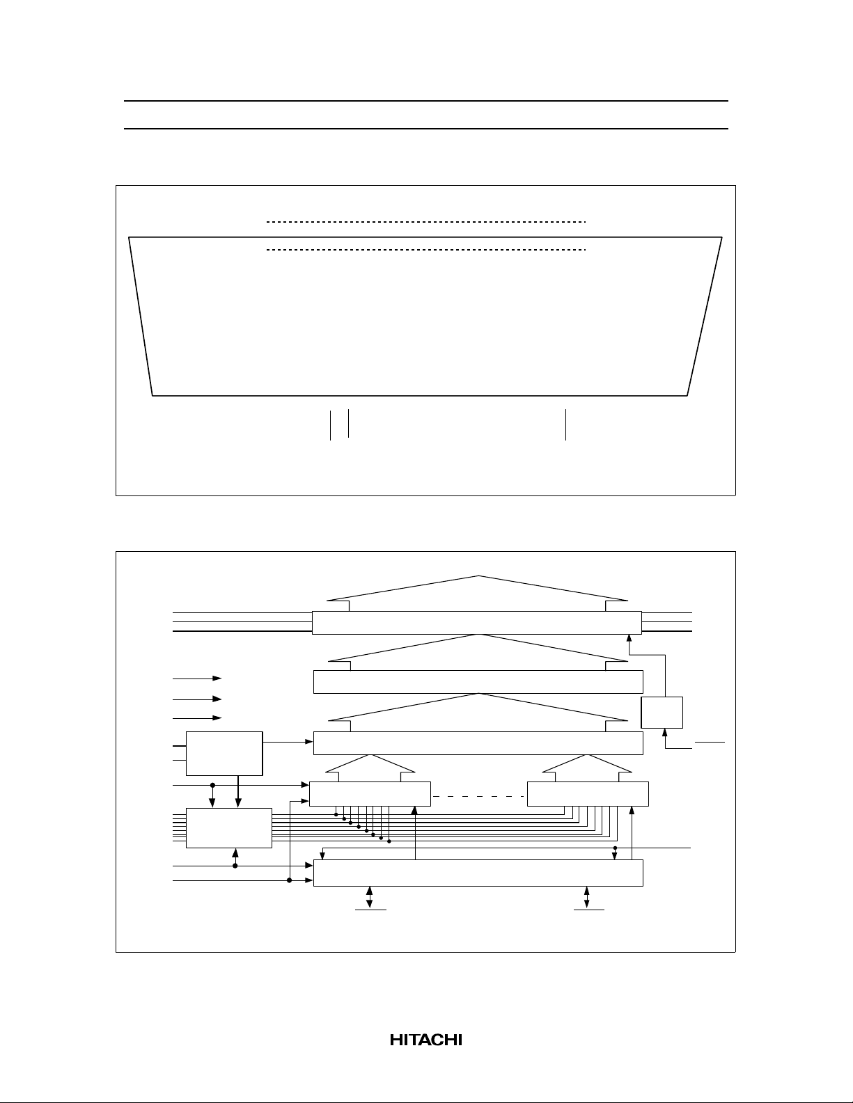
Internal Block Diagram
346
VML
4Y4
5Y5
345
344
343
V0L
V1L
VCCMODEBSGND2
342
341
340
339
SHL
Top View
338
337
336
335
334
333
332
331
EIO1
DISPD0D1D2D3D4D5D6D7
330
329
328
CL2
327
326
325
324
CL1MEIO2
GND1
316 Y316
317 Y317
323
V1R
318 Y318
322
V0R
319 Y319
321
VMR
320 Y320
Y1–Y
320
V0L
VML
V1L
Vcc
GND2
GND1
CL1
M
BS
D0–D7
SHL
MODE
Note: Pins V0L, VML, and V1L are internally connected to pins V0R, VMR, and V1R, respectively.
Timing
generator
circuit
Data
rearrangement
circuit
Liquid crystal drive circuit
Level shifter
Level
shifter
Latch circuit 2
Latch circuit 1Latch circuit 1
Shift register
EIO1 EIO2
*
V0L
VML
V1L
DISP
CL2
2
Page 3
HD66130T
1. Liquid crystal drive circuit
Selects and outputs the liquid crystal drive level V0, VM, or V1 by DISP and a combination of data for
latch circuit 2 and signal M.
2. Level shifter
Converts logic signals to liquid crystal drive signals.
3. Latch circuit 2
320-bit latch circuit, which latches the data of latch circuits 1 at the fall of CL1 and outputs the data to
the level shifter.
4. Latch circuit 1
4/8-bit parallel data latch circuit, which latches display data D0 to D7 according to signals transmitted
from the shift register.
5. Shift register
80-bit shift register, which generates data-capture signals for latch circuits 1 at the fall of CL2.
6. Data rearrangement circuit
Inverts the order of data output crosswise.
7. Timing generator circuit
The timing generator circuit generates data latch pulses for latch circuit2 and changes pulse the LCD
drive outputs to AC.
HIFAS Family timing Comparision
HD66130/131/134/135 HD66132/133
Input
CL1
signal
M
Output
signal
Segment
Common
3
Page 4
HD66130T
Pin Functions
Class Symbol
Power
supply
V
CC
GND1
GND2
V0L, R
VML, R
V1L, R
Control
CL1 327 Clock 1 Input Latch signal of display data: A liquid crystal drive signal
signal
CL2 328 Clock 2 Input Capture signal of display data: Display data is captured
M 326 M Input A.C. signal of liquid crystal drive output
D0 to D7 336 to
SHL 339 Shift Left Input Control signal for inverting the order of data output
EIO1 338 Enable
Pin
Number
343
324
340
345, 322
346, 321
344, 323
329
Pin
Name I/O Functions
V
CC
—V
–GND: Power supply for logic.
CC
GND
V0L, R
Input Liquid crystal drive level power supply
VML, R
V1L, R
corresponding to display data is output at the fall of CL1.
at the fall of CL2.
DATA 0
to
Input
Display data Liquid crystal drive output Liquid crystal display
1 (Vcc level) Selected level ON
DATA 7
(see the following page)
I/O
IO1
SHL
GND
Vcc
V0
VM
V1
OFFNot-selected level0 (GND level)
EI/O1 EI/O2
Enable input
Enable output Enable input
Enable output
EIO2 325 Enable
IO2
I/O Enable input: The enable input of the first IC is
connected to the GND and another is connected to the
enable output of the second IC.
Enable output: Connected to the enable input of the
second IC at cascade output.
DISP 337 Disp off Input Grounding DISP sets liquid crystal drive output Y1–Y320
to the VM level.
BS 341 Bus
Select
Input Switches the number of input bits for the display data.
Vcc
8-bit input mode
GND
4-bit input mode (Captures data from D0–D3. At this
time, connect D4–D7 to the GND.)
MODE 342 MODE Input Switches the number of input bits for the display data.
Vcc
320 output mode
GND
240 output mode (Y41–Y280 are valid output. The
other 80 pins output the not-selected-level signals
synchronized every time; release these pins.)
4
Page 5
Pin Functions (cont)
HD66130T
Class Symbol
Liquid crystal
drive output
Y1 to
Y320
Pin
Number
1 to 320 Y1 to
Pin
Name I/O Function
Y320
Output Liquid crystal drive output: Selects and outputs level
V0 or V1 according to the combination of the M signal
and display data when DISP is connected to Vcc.
M
D
Output level
1
00
11
V0 V1 V1 V0
0
5
Page 6

HD66130T
Rearranging Output Data (SHL)
The order for the output of captured data is inverted crosswise according to the SHL signal. At this time,
the input/output pin of the enable signal can be switched.
SHL = GND, BS = GND
Y314
Y314
Y315
Y315
Y1
SHL = Vcc, BS = GND
Y1
Y3
Y2
First data Last data
Y3
Y2
Y4
Y4
Y5
Y5
Y7
Y6
Y6
Y8
D0D3 D2D2 D1 D0 D3 D1 D3 D2D2 D1 D0 D3 D1 D0
Enable input: EIO1
Enable output: EIO2
Y7
Y8
D3D0 D1D1 D2 D3 D0 D2 D0 D1D1 D2 D3 D0 D2 D3
Y313 Y319
Y313 Y319
Y316
Y316
Y317
Y317
Y318
Y318
Y320
Y320
Last data First data
Enable input: EIO2
Enable output: EIO1
SHL = GND, BS = Vcc
Y1
SHL = Vcc, BS = Vcc
Y1
Y2
Y2
Y3
Y4
First data Last data
Y3
Y4
Last data First data
Y5
Y5
Y7
Y6
Y6
Y8
D0D7 D2D6 D5 D4 D3 D1 D7 D2D6 D5 D4 D3 D1 D0
Enable input: EIO1
Enable output: EIO2
Y7
Y8
D7D0 D5D1 D2 D3 D4 D6 D0 D5D1 D2 D3 D4 D6 D7
Enable input: EIO2
Enable output: EIO1
Y314
Y314
Y315
Y315
Y313 Y319
Y313 Y319
Y316
Y316
Y317
Y317
Y318
Y318
Y320
Y320
6
Page 7

Operation Timing
(1) 4-bit capture mode (1 line, 640 dots)
CL2
12 159 160
HD66130T
Line
81 828079 161
D0
to
D3
CL1
EIO2
(No. 1)
EIO2
(No. 2)
Y1–Y320
d4d1d8
d5
Data capture period
for IC (No. 1)
BS = GND (4-bit capture mode)
d316
d313
d320
d317
Data capture period for IC
(No. 2)
During the data standby state when the data capture operation enable signal is low (SHL = GND: EIO1),
the next data capture clock (CL2) cancels the standby state. The 4-bit data is captured at the fall of CL2.
When 316 bits are captured, the enable signal becomes the GND level (SHL = GND: EIO2). When 320
bits are captured, the operation automatically stops (the standby state is entered). The second IC is then
activated when pin EIO2 is connected to pin EIO1 of the second IC.
Data output changes at the fall of CL1.
During SHL = GND, captured data d1 and d320 are output to Y1 and Y320, respectively. During SHL =
Vcc, data d1 and d320 are output to Y320 and Y1, respectively.
7
Page 8

HD66130T
(2) 8-bit capture mode (1 line, 640 dots)
CL2
12 79 80
D0
to
D7
CL1
EIO2
(No. 1)
d8d1d16
d9
Data capture period
for IC (No. 1)
d312
d305
Line
41 424039
d320
d313
EIO2
(No. 2)
Data capture period for
IC (No. 2)
Y1–Y320
BS = Vcc (8-bit capture mode)
The 8-bit display data is captured at the fall of CL2. Other basic operations are the same as those of the 4bit capture mode.
8
Page 9

Application Example
HD66130T
VLL, R
VML, R
VHL, R
VLCDL, R
VEEL, R
DIO1
DISP
SHL
MWS4–0
M
GND
CL
Vcc
MODE
VLCD
VH (COM)
Vcc
V0 (SEG)
VM
V1 (SEG)
GND
VL (COM)
VEE
COM1
COM2
COM3
COM4
COM5
X240 to X1
HD66131T
COM236
COM237
COM238
COM239
COM240
Power supply
circuit
EIO2
GND1,2
SEG1
M
SEG2
CL1
SEG3
SEG4
SEG5
Y320 to Y1
HD66130T
D7
–
CL2
D0
DISP
EIO1
SHL
LCD Panel
640 x 240
1/240 duty
MODE
Vcc
BS
V1L, R
V0L, R
GND1,2
VML, R
EIO2
M
Y320 to Y1
HD66130T
CL2
CL1
D7
–
D0
DISP
EIO1
SHL
BS
Vcc
MODE
SEG636
SEG637
SEG638
V1L, R
SEG639
SEG640
VML, R
V0L, R
M
D7
–
DISP
D0
CL2
FLM
CL1
Controller
Notes:
1. When designing the board, connect a capacitor near the IC to stabilize power supply. Use two capacitors of about
0.1 µF for each IC (between Vcc and GND, V0 and GND, VLCD and GND, and V
and GND).
EE
2. In addition, for the power supply circuit, connect a capacitor of several µF or several tens of µF between the liquid
crystal power supply and GND. For set evaluation, confirm that there is no inversion of liquid crystal drive power
supply and level power supply in the period between when the liquid crystal drive power supply is turned on and
when it is turned off.
3. Configuring the LCD panel using the HD66130 when using the select COMMON driver.
The select COMMON driver
COMMON driver select
HD66131 (240OUT) ●
HD66133 (120OUT) ×
HD66135 (120OUT) ●
9
Page 10

HD66130T
Absolute Maximum Ratings
Item Symbol Rating Unit Notes
Power supply voltage for logic circuits V
CC
Power supply voltage for LCD drive circuits V0 –0.3 to + 7.0 V 1, 4
Input voltage 1 VT1 –0.3 to VCC + 0.3 V 1, 2
Input voltage 2 VT2 –0.3 to V0 + 0.3 V 1, 3, 4
Operating temperature T
Storage temperature T
opr
stg
Notes: 1. Potential from the GND
2. Applied to pins SHL, EIO1, EIO2 , DISP, D0 to D7, CL1, CL2, M, BS, and MODE.
3. Applied to VML, VMR, V1L, and VMR.
Operating the LSI in excess of the absolute maximum rating will result in permanent damage.
Use the LSI observing electrical characteristic conditions in normal operation. Exceeding the
conditions will cause malfunctions or will affect LSI reliability.
4. Conform to the following turn-on/off sequence of the power and signals. Otherwise, the LSI will
malfunction or will be permanently damaged. In addition, LSI reliability will be affected.
–0.3 to + 7.0 V 1, 4
–30 to +75 °C
–55 to +110 °C
Vcc
V0
VM
V1
DISP
Input-signal
clock data
2.7 V
0ms
Signal-undefined
period
0ms
VM
V1
0ms 0ms
Initialization period
(at least one frame)
2.7 V
0ms
0ms
(0 ms: Minimum value)
10
Page 11

HD66130T
4.1 Turning on the power
1) Turn on the power in the order of GND- VCC, GND-V0, and VM/V1. Then, ground the DISP pin.
2) The LCD forcibly outputs the VM level by the DISPOFF function.
3) Even if an input signal is disturbed immediately after VCC is applied, the DISPOFF function has priority.
4) Input the specific signal to initialize registers in the driver. The initialization period must be at least one
frame.
5) The preparation of normal display is completed. Input the VCC level to the DISP pin to cancel the
DISPOFF function. At this time, the level of pins V0, VM, and V1 must rise to the specific potential.
4.2 Turning off the power
The procedure is basically the reverse for turning on the power.
1) Ground the DISP pin.
2) Turn off the liquid crystal power in the order of VM/V1 and GND-V0.
3) Ground VCC and an input signal.
At this time, the level of pins V0, VM, and V1 must fall to 0 V. Since the DISPOFF function stops when
VCC falls to 0 V, the LCD may output a level other than VM. Therefore, a display failure may occur when
the power is turned off or on.
11
Page 12

HD66130T
Electrical Characteristics
DC Characteristics 1 (VCC = 2.5 to 4.5V, V0–GND = 2.6 to 5.5V, Ta = –30 to +75°C)
Item Symbol Pins Min Typ Max Unit Test Condition Notes
Input high voltage VIH CL1,
0.8 × V
CL2,
SHL,
M,
EIO1,
EIO2,
Input low voltage VIL MODE,
0 — 0.2 × V
DISP,
D0 to
D7, BS
Output high voltage VOH EIO1,
VCC –0.4 — — V IOH = –0.4 mA
EIO2
Output low voltage VOL EIO1,
— — 0.4 V I
EIO2
Vi–Yj on resistance R
ON
Y1 to
— 0.7 2.0 kΩ ION = 150 µA1
Y320,
V0L, R
Y1 to
— 2.0 3.0 kΩ
Y320,
VML, R
Y1 to
— 0.7 2.0 kΩ
Y320,
V1L, R
Input leakage current 1 I
IL1
CL1,
–5.0 5.0 µA VIN = V
CL2,
SHL,
M,
EIO1,
EIO2,
MODE,
DISP,
D0 to
D7, BS
Input leakage current 2 I
IL2
VML,
–25 25 µA VIN = V0 to GND
R,
V1L, R
Current consumption 1 I
CC
V
— 150 300 µAVCC = 3.3 V
CC
Current consumption 2 IV0 V0L, R — 60 200 µAf
Current consumption 3 I
ST
V
— 50 100 µA fM = 1.5 kHz 2, 3
CC
—V
CC
CC
V
V
CC
= 0.4 mA
OL
to GND
CC
2
V0 = 2.7 V
= 3.5 MHz
CL2
f
= 19.2 kHz
CL1
12
Page 13

HD66130T
DC Characteristics 2 (VCC = 4.5 to 5.5V, V0–GND = 2.6 to 5.5V, Ta = –30 to +75°C)
Item Symbol Pins Min Typ Max Unit Test Condition Notes
Input high voltage VIH CL1,
0.8 × V
CL2,
SHL,
M,
EIO1,
EIO2,
Input low voltage VIL MODE,
0 — 0.2 × V
DISP,
D0 to
D7, BS
Output high voltage VOH EIO1,
VCC –0.4 — — V IOH = –0.4 mA
EIO2
Output low voltage VOL EIO1,
— — 0.4 V I
EIO2
Vi–Yj on resistance R
ON
Y1 to
— 0.7 2.0 kΩ ION = 150 µA1
Y320,
V0L, R
Y1 to
— 2.0 3.0 kΩ
Y320,
VML, R
Y1 to
— 0.7 2.0 kΩ
Y320,
V1L, R
Input leakage current 1 I
IL1
CL1,
–5.0 5.0 µA VIN = V
CL2,
SHL,
M,
EIO1,
EIO2,
MODE,
DISP,
D0 to
D7, BS
Input leakage current 2 I
IL2
VML,
–25 25 µA VIN = V0 to GND
R,
V1L, R
Current consumption 1 I
CC
V
— 230 450 µAVCC = 5.0 V
CC
Current consumption 2 IV0 V0L, R — 60 200 µAf
Current consumption 3 I
ST
V
— 80 150 µA fM = 1.5 kHz 2, 3
CC
Notes: 1. Resistance between pins Y and V when a load current flows to one of the pins from Y1 to Y320.
The following conditions are defined:
V0–GND = 5.5 V
VM = (V0 + V1)/2
—V
CC
CC
V
V
CC
= 0.4 mA
OL
to GND
CC
2
V0 = 2.7 V
= 3.5 MHz
CL2
f
= 19.2 kHz
CL1
13
Page 14

HD66130T
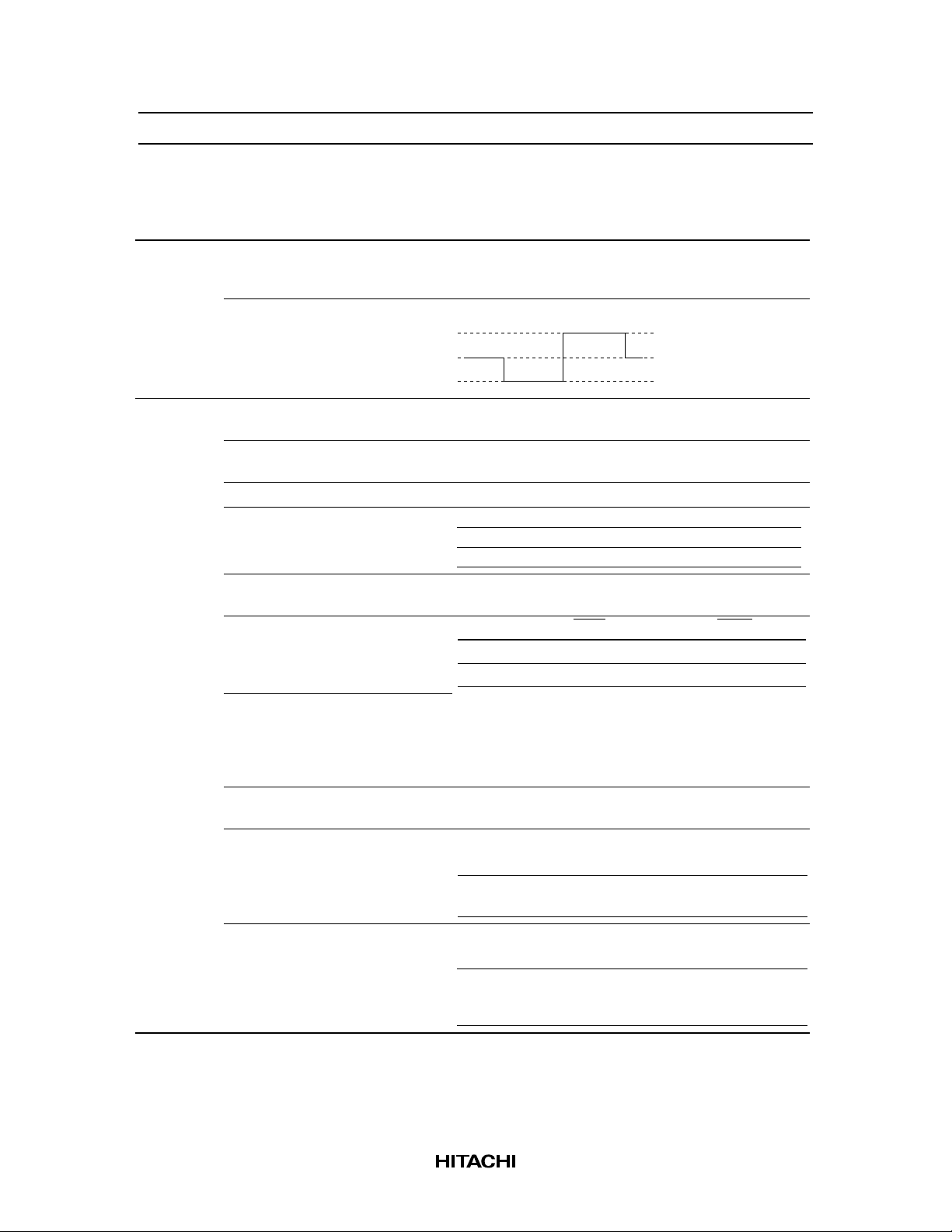
V1 = GND + 1.0
The voltage range of the liquid crystal drive level power supply is described. A voltage around
the GND is applied to pin V1, and an intermediate voltage of about V0 and V1 is applied to pin
VM. Use the V1 in the range of ∆V = 0.25 x V0, in which the impedance Ron of driver output is
stable.
V0
VM
∆V = 0.25 x V0
V1
GND
Relationship between the driver output waveform and each level voltage
2. A current flowing in the input or output section is excluded. If an input signal is at an
intermediate level for the CMOS, a through-current flows in the input circuit and power supply
current increases. Therefore, VIH must be at the Vcc level and VIL must be at the GND level.
3. Current at standby
4. The voltage of each signal is shown below.
Segment
voltage
V0 (5.0 V)
Vcc (3.3 V)
VM (3.0 V)
V1 (1.0 V)
GND (0.0 V)
Segment waveform
Common waveform
Common
voltage
VH (23.0 V)
Vcc (3.3 V)
VM (3.0 V)
GND (0.0 V)
14
Normal display period
Display-off
period
Normal display period
VL (–17.0 V)
Display-off
period
Page 15

HD66130T
AC Characteristics 1 (VCC = 2.5 to 4.5V, V0–GND = 2.6 to 5.5V, Ta = –30 to +75°C)
Item Symbol Pins Min Max Unit
Clock cycle time t
Clock high pulse width 1 t
Clock low pulse width 1 t
Clock high pulse width 2 t
Clock setup time t
Clock hold time t
Clock rise time t
Clock fall time t
Data setup time t
Data hold time t
M setup time t
M hold time t
Output delay time 1 t
CYC
CWH2
CWL2
CWH1
SCL
HCL
r
f
DS
DH
MS
MH
pd1
AC Characteristics 2 (VCC = 4.5V to 5.5V, V0–GND = 2.6 to 5.5V, Ta = –30 to +75°C)
CL2 152 — ns
CL2 65 — ns
CL2 65 — ns
CL1 65 — ns
CL1, CL2 80 — ns
CL1, CL2 80 — ns
CL1, CL2 — 30 ns
CL1, CL2 — 30 ns
D0 to D7, CL2 50 — ns
D0 to D7, CL2 50 — ns
M, CL1 20 — ns
M, CL1 20 — ns
CL1, Y1 to Y320 — 1000 ns
Item Symbol Pins Min Max Unit
Clock cycle time t
Clock high pulse width 1 t
Clock low pulse width 1 t
Clock high pulse width 2 t
Clock setup time t
Clock hold time t
Clock rise time t
Clock fall time t
Data setup time t
Data hold time t
M setup time t
M hold time t
Output delay time 1 t
CYC
CWH2
CWL2
CWH1
SCL
HCL
r
f
DS
DH
MS
MH
pd1
CL2 125 — ns
CL2 45 — ns
CL2 45 — ns
CL1 45 — ns
CL1, CL2 80 — ns
CL1, CL2 80 — ns
CL1, CL2 — 20 ns
CL1, CL2 — 20 ns
D0 to D7, CL2 20 — ns
D0 to D7, CL2 20 — ns
M, CL1 20 — ns
M, CL1 20 — ns
CL1, Y1 to Y320 — 1000 ns
Notes: 1. A load must be 10 pF or less for EI/O connection between drivers.
2. For output delay time 1 and 2, connect the load circuit shown below.
Test point
100 pF
15
Page 16

HD66130T
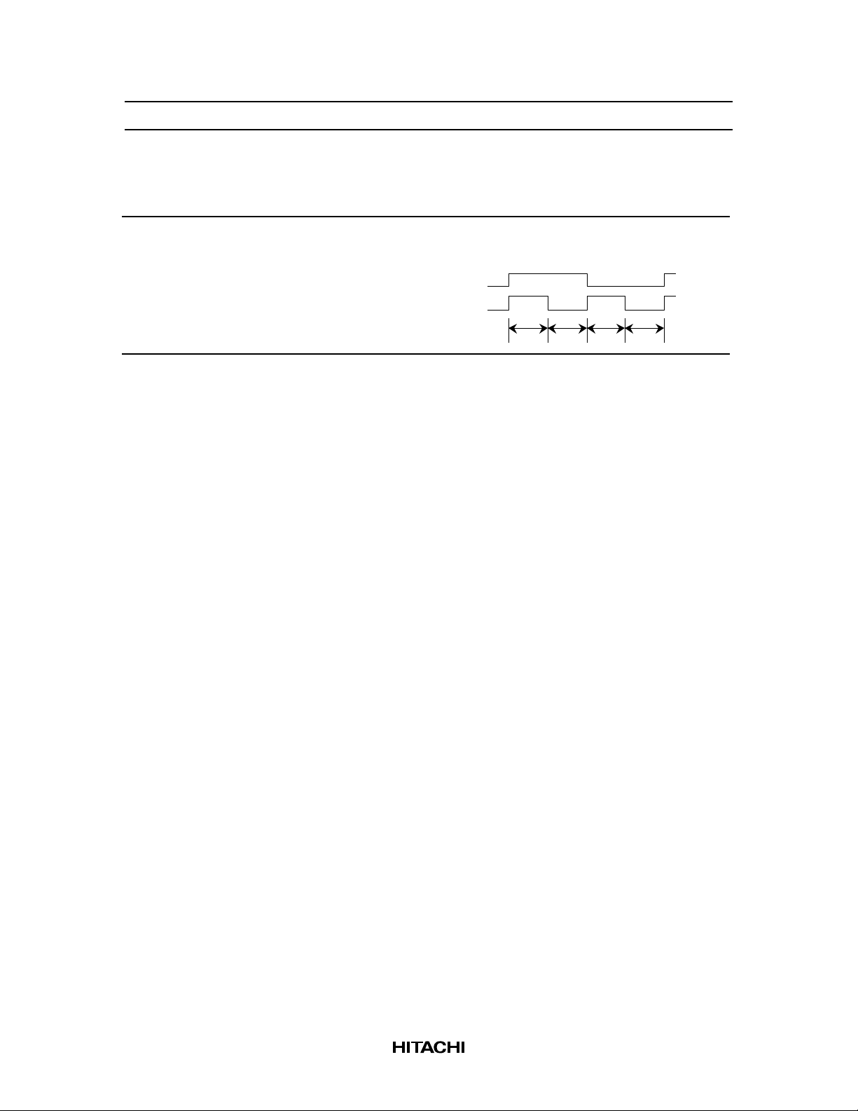
CL2
D0–7
CL1
tr t
0.2 Vcc
CWH2
0.8 Vcc
t
DS
0.8 Vcc
0.2 Vcc
tf t
t
CWH1
CWL2
t
DH
t
SCL
0.8 Vcc
0.2 Vcc
t
HCL
t
CYC
CL2
M
CL1
Y (n)
t
MS
0.8 Vcc
0.2 Vcc
t
MH
0.2 Vcc
t
pd1
0.2 Vcc
0.8 V0
0.2 V1
16
 Loading...