

Page 1

SH7708 Series
SH7708, SH7708S, SH7708R
Hardware Manual
ADE-602-105E
Rev.6.0
5/5/99
Hitachi, Ltd.
Page 2

Cautions
1. Hitachi neither warrants nor grants licenses of any rights of Hitachi’s or any third party’s
patent, copyright, trademark, or other intellectual property rights for information contained in
this document. Hitachi bears no responsibility for problems that may arise with third party’s
rights, including intellectual property rights, in connection with use of the information
contained in this document.
2. Products and product specifications may be subject to change without notice. Confirm that you
have received the latest product standards or specifications before final design, purchase or use.
3. Hitachi makes every attempt to ensure that its products are of high quality and reliability.
However, contact Hitachi’s sales office before using the product in an application that demands
especially high quality and reliability or where its failure or malfunction may directly threaten
human life or cause risk of bodily injury, such as aerospace, aeronautics, nuclear power,
combustion control, transportation, traffic, safety equipment or medical equipment for life
support.
4. Design your application so that the product is used within the ranges guaranteed by Hitachi
particularly for maximum rating, operating supply voltage range, heat radiation characteristics,
installation conditions and other characteristics. Hitachi bears no responsibility for failure or
damage when used beyond the guaranteed ranges. Even within the guaranteed ranges, consider
normally foreseeable failure rates or failure modes in semiconductor devices and employ
systemic measures such as fail-safes, so that the equipment incorporating Hitachi product does
not cause bodily injury, fire or other consequential damage due to operation of the Hitachi
product.
5. This product is not designed to be radiation resistant.
6. No one is permitted to reproduce or duplicate, in any form, the whole or part of this document
without written approval from Hitachi.
7. Contact Hitachi’s sales office for any questions regarding this document or Hitachi
semiconductor products.
Page 3

Preface
The SH7708, SH7708S, and SH7708R(SH7708 Series) use a RISC (reduced instruction set
computer) type CPU to achieve high-performance computational processing. Also incorporating
the peripheral functions required for system configuration plus power-down features essential for
microcontroller application systems, the SH7708 Series is a new-generation RISC microcontroller
(SuperH RISC engine).
The SH7708 Series have a RISC type instruction set, with basic instructions executed in one
state, offering a drastic improvement in instruction execution speed. It also has an on-chip 32-bit
multiplier (producing a 64-bit result) capable of high-speed multiply-and-accumulate operations.
The SH7708 Series’s instructions are upward-compatible with those of the SH-1 and SH-2,
facilitating migration from these series to the SH7708 Series.
SH7708R is completely pin compatible with the SH7708S. On-chip supporting modules that
enable a user system to be configured with a minimum of components include oscillation circuits,
an interrupt controller (INTC), timers, a realtime clock (RTC), and a serial communication
interface (SCI). A user break controller (UBC) is provided as an on-chip module supporting
program development, allowing easy configuration of a simple debugger.
On-chip cache memory improves CPU processing performance, and a built-in memory
management unit (MMU) performs address translation between a 4-gigabyte virtual space and
physical space. An on-chip bus state controller (BSC) provides more efficient external memory
access, and enables direct connection to synchronous DRAM, DRAM, and pseudo-SRAM without
the need for glue logic.
This hardware manual describes the hardware of the SH7708 Series. Details of instructions can be
found in the programming manual.
Related Manuals
SH7708Series instructions
SH-3/SH-3E/SH3-DSP Programming Manual
Please consult your Hitachi sales representative for details of development environment system.
Page 4

Page 5

Contents
Section 1 Overview and Pin Functions ...............................................1
1.1 SH7708 Series Features ........................................................................................1
1.2 Block Diagram....................................................................................................6
1.3 Pin Description ...................................................................................................7
1.3.1 Pin Arrangement......................................................................................7
1.3.2 SH7708 Series Pin Functions.....................................................................8
Section 2 CPU .......................................................................... 13
2.1 Register Configuration..........................................................................................13
2.1.1 Privileged Mode and Banks.........................................................................13
2.1.2 General Registers .....................................................................................16
2.1.3 System Registers .....................................................................................17
2.1.4 Control Registers .....................................................................................17
2.2 Data Formats ......................................................................................................19
2.2.1 Data Format in Registers ...........................................................................19
2.2.2 Data Format in Memory ............................................................................19
2.3 Instruction Features..............................................................................................20
2.3.1 Execution Environment .............................................................................20
2.3.2 Addressing Modes.....................................................................................22
2.3.3 Instruction Formats ..................................................................................26
2.4 Instruction Set.....................................................................................................29
2.4.1 Instruction Set Classified by Function..........................................................29
2.4.2 Instruction Code Map................................................................................45
2.5 Processor States and Processor Modes......................................................................48
2.5.1 Processor States .......................................................................................48
2.5.2 Processor Modes ......................................................................................49
Section 3 Memory Management Unit (MMU)....................................... 51
3.1 Overview............................................................................................................51
3.1.1 Features..................................................................................................51
3.1.2 Role of MMU .........................................................................................51
3.1.3 SH7708 Series MMU ...............................................................................54
3.1.4 Register Configuration..............................................................................57
3.2 Register Description.............................................................................................58
3.3 TLB Functions ....................................................................................................60
3.3.1 Configuration of the TLB ..........................................................................60
3.3.2 TLB Indexing..........................................................................................62
3.3.3 TLB Address Comparison..........................................................................63
3.3.4 Page Management Information....................................................................65
1
Page 6

3.4 MMU Functions .................................................................................................66
3.4.1 MMU Hardware Management..................................................................... 66
3.4.2 MMU Software Management .....................................................................66
3.4.3 MMU Instruction (LDLTB) .......................................................................67
3.4.4 Avoiding Synonym Problems ....................................................................68
3.5 MMU Exceptions ................................................................................................ 70
3.5.1 TLB Miss Exception ................................................................................70
3.5.2 TLB Protection Violation Exception............................................................71
3.5.3 TLB Invalid Exception..............................................................................72
3.5.4 Initial Page Write Exception ......................................................................73
3.5.5 Processing Flow in Event of MMU Exception (Same Processing Flow for Address
Error) .........................................................................................................75
3.6 Memory-Mapped TLB..........................................................................................77
3.6.1 Address Array..........................................................................................77
3.6.2 Data Array..............................................................................................78
3.6.3 Usage Examples ......................................................................................80
3.7 Usage Note.........................................................................................................80
Section 4 Exception Handling.........................................................81
4.1 Overview...........................................................................................................81
4.1.1 Features .................................................................................................81
4.1.2 Register Configuration..............................................................................81
4.2 Exception Handling Function.................................................................................81
4.2.1 Exception Handling Flow..........................................................................81
4.2.2 Exception Handling Vector Addresses...........................................................82
4.2.3 Acceptance of Exceptions.......................................................................... 84
4.2.4 Exception Codes......................................................................................86
4.2.5 Exception Request Masks..........................................................................87
4.2.6 Returning from Exception Handling ............................................................88
4.3 Register Description.............................................................................................88
4.4 Exception Handler Operation..................................................................................89
4.4.1 Reset ..................................................................................................... 89
4.4.2 Interrupts................................................................................................89
4.4.3 General Exceptions...................................................................................89
4.5 Individual Exception Operations.............................................................................90
4.5.1 Resets....................................................................................................90
4.5.2 General Exceptions...................................................................................91
4.5.3 Interrupts................................................................................................94
4.6 Cautions ............................................................................................................95
Section 5 Cache .........................................................................97
5.1 Overview...........................................................................................................97
5.1.1 Features .................................................................................................97
2
Page 7

5.1.2 Cache Structure........................................................................................97
5.1.3 Register Configuration..............................................................................99
5.2 Register Description.............................................................................................99
5.2.1 Cache Control Register (CCR) ...................................................................99
5.3 Cache Operation..................................................................................................100
5.3.1 Searching the Cache..................................................................................100
5.3.2 Read Access............................................................................................102
5.3.3 Write Access ...........................................................................................102
5.3.4 Write-Back Buffer.....................................................................................102
5.3.5 Coherency of Cache and External Memory....................................................103
5.3.6 RAM Mode.............................................................................................103
5.4 Memory-Mapped Cache.........................................................................................103
5.4.1 Address Array..........................................................................................103
5.4.2 Data Array..............................................................................................104
5.5 Usage Examples ..................................................................................................106
5.5.1 Invalidating Specific Entries.......................................................................106
5.5.2 Reading the Data of a Specific Entry............................................................106
Section 6 Interrupt Controller (INTC)................................................ 107
6.1 Overview............................................................................................................107
6.1.1 Features..................................................................................................107
6.1.2 Block Diagram.........................................................................................108
6.1.3 Pin Configuration ....................................................................................109
6.1.4 Register Configuration..............................................................................109
6.2 Interrupt Sources..................................................................................................109
6.2.1 NMI Interrupts.........................................................................................110
6.2.2 IRL Interrupts..........................................................................................110
6.2.3 On-Chip Supporting Module Interrupts ........................................................112
6.2.4 Interrupt Exception Handling and Priority.....................................................112
6.3 INTC Registers ...................................................................................................115
6.3.1 Interrupt Priority Registers A and B (IPRA–IPRB).........................................115
6.3.2 Interrupt Control Register (ICR) .................................................................116
6.4 INTC Operation...................................................................................................117
6.4.1 Interrupt Sequence....................................................................................117
6.4.2 Multiple Interrupts ...................................................................................119
6.5 Interrupt Response Time .......................................................................................120
Section 7 User Break Controller (UBC)............................................. 123
7.1 Overview............................................................................................................123
7.1.1 Features..................................................................................................123
7.1.2 Block Diagram.........................................................................................123
7.1.3 Register Configuration..............................................................................125
7.1.4 Break Conditions and Register Settings ........................................................125
3
Page 8

7.2 UBC Register Functions ....................................................................................... 126
7.2.1 Break Address Register A (BARA)...............................................................126
7.2.2 Break Address Register B (BARB)............................................................... 126
7.2.3 Break ASID Register A (BASRA)...............................................................127
7.2.4 Break ASID Register B (BASRB)................................................................ 127
7.2.5 Break Address Mask Register A (BAMRA)................................................... 127
7.2.6 Break Address Mask Register B (BAMRB).................................................... 128
7.2.7 Break Bus Cycle Register A (BBRA)...........................................................128
7.2.8 Break Bus Cycle Register B (BBRB)............................................................ 129
7.2.9 Break Data Register B (BDRB)................................................................... 130
7.2.10 Break Data Mask Register B (BDMRB)......................................................131
7.2.11 Break Control Register (BRCR)................................................................132
7.3 UBC Operation ...................................................................................................134
7.3.1 User Break Operation Flow........................................................................134
7.3.2 Instruction Fetch Cycle Break.....................................................................135
7.3.3 Data Access Cycle Break........................................................................... 136
7.3.4 Saved Program Counter (PC) Value.............................................................137
7.3.5 Examples of Use......................................................................................138
7.3.6 Cautions ................................................................................................140
Section 8 Power-Down Modes........................................................141
8.1 Overview...........................................................................................................141
8.1.1 Power-Down Modes................................................................................. 141
8.1.2 Register Configuration..............................................................................142
8.1.3 Pin Configuration .................................................................................... 143
8.2 Register Description.............................................................................................143
8.2.1 Standby Control Register (STBCR).............................................................143
8.3 Sleep Mode ........................................................................................................145
8.3.1 Transition to Sleep Mode ..........................................................................145
8.3.2 Canceling Sleep Mode ..............................................................................145
8.4 Standby Mode.....................................................................................................145
8.4.1 Transition to Standby Mode.......................................................................145
8.4.2 Canceling Standby Mode...........................................................................146
8.4.3 Clock Pause Function...............................................................................147
8.5 Module Standby Function .....................................................................................147
8.5.1 Transition to Module Standby Function ....................................................... 147
8.5.2 Clearing the Module Standby Function........................................................148
8.6 Timing of STATUS Pin Changes...........................................................................148
8.6.1 Timing for Resets .................................................................................... 148
8.6.2 Timing for Canceling Standbys ..................................................................150
8.6.3 Timing for Canceling Sleep Mode...............................................................151
8.7 Hardware Standby Mode........................................................................................153
8.7.1 Transition to Hardware Standby Mode.......................................................... 153
4
Page 9

8.7.2 Canceling Hardware Standby Mode..............................................................154
8.7.3 Hardware Standby Mode Timing..................................................................154
Section 9 On-Chip Oscillation Circuits............................................... 157
9.1 Overview............................................................................................................157
9.1.1 Features..................................................................................................157
9.2 Overview of the CPG ...........................................................................................158
9.2.1 CPG Block Diagram.................................................................................158
9.2.2 CPG Pin Configuration.............................................................................161
9.2.3 CPG Register Configuration ......................................................................161
9.3 Clock Operating Modes.........................................................................................162
9.4 Register Descriptions............................................................................................170
9.4.1 Frequency Control Register (FRQCR)..........................................................170
9.5 Changing the Frequency........................................................................................174
9.5.1 Changing the Multiplication Rate ...............................................................174
9.5.2 Changing the Division Ratio......................................................................174
9.6 PLL Standby Function..........................................................................................175
9.6.1 Overview of the PLL Standby Function........................................................175
9.6.2 Usage.....................................................................................................175
9.7 Controlling Clock Output .....................................................................................176
9.7.1 Clock Modes 0–2 .....................................................................................176
9.7.2 Clock Modes 3 and 4 ................................................................................176
9.8 Overview of the Watchbog Timer (WDT).................................................................177
9.8.1 Block Diagram of the WDT........................................................................177
9.8.2 Register Configurations.............................................................................177
9.9 WDT Registers....................................................................................................178
9.9.1 Watchdog Timer Counter (WTCNT)............................................................178
9.9.2 Watchdog Timer Control/Status Register (WTCSR) .......................................178
9.9.3 Notes on Register Access...........................................................................180
9.10 Using the WDT .................................................................................................181
9.10.1 Canceling Standbys.................................................................................181
9.10.2 Changing the Frequency...........................................................................181
9.10.3 Using Watchdog Timer Mode....................................................................182
9.10.4 Using Interval Timer Mode.......................................................................182
9.10.5 Usage Notes ..........................................................................................183
9.11 Notes on Board Design........................................................................................184
Section 10 Bus State Controller (BSC) .............................................. 187
10.1 Overview..........................................................................................................187
10.1.1 Features ................................................................................................187
10.1.2 Block Diagram.......................................................................................188
10.1.3 Pin Configuration...................................................................................190
10.1.4 Register Configuration ............................................................................192
5
Page 10

10.1.5 Area Overview.......................................................................................193
10.1.6 PCMCIA Support .................................................................................. 196
10.2 BSC Registers...................................................................................................200
10.2.1 Bus Control Register 1 (BCR1) ................................................................200
10.2.2 Bus Control Register 2 (BCR2) ................................................................203
10.2.3 Wait State Control Register 1 (WCR1) ......................................................204
10.2.4 Wait State Control Register 2 (WCR2) ......................................................205
10.2.5 Individual Memory Control Register (MCR) ...............................................208
10.2.6 DRAM Control Register (DCR) ...............................................................213
10.2.7 PCMCIA Control Register (PCR).............................................................215
10.2.8 Synchronous DRAM Mode Register (SDMR) .............................................216
10.2.9 Refresh Timer Control/Status Register (RTCSR).........................................217
10.2.10 Refresh Timer Counter (RTCNT) ............................................................219
10.2.11 Refresh Time Constant Register (RTCOR)................................................220
10.2.12 Refresh Count Register (RFCR)..............................................................220
10.2.13 Cautions on Accessing Refresh Control Related Registers............................221
10.3 BSC Operation..................................................................................................222
10.3.1 Endian/Access Size and Data Alignment.....................................................222
10.3.2 Description of Areas ...............................................................................228
10.3.3 Basic Interface........................................................................................231
10.3.4 DRAM Interface.....................................................................................237
10.3.5 Synchronous DRAM Interface..................................................................253
10.3.6 Pseudo-SRAM Direct Connection ............................................................. 269
10.3.7 Burst ROM Interface............................................................................... 278
10.3.8 PCMCIA Interface..................................................................................281
10.3.9 Waits between Access Cycles...................................................................293
10.3.10 Bus Arbitration ....................................................................................294
Section 11 Timer (TMU)...............................................................297
11.1 Overview..........................................................................................................297
11.1.1 Features................................................................................................297
11.1.2 Block Diagram.......................................................................................297
11.1.3 Pin Configuration ..................................................................................299
11.1.4 Register Configuration............................................................................299
11.2 TMU Registers..................................................................................................300
11.2.1 Timer Output Control Register (TOCR).....................................................300
11.2.2 Timer Start Register (TSTR) .................................................................... 301
11.2.3 Timer Control Register (TCR)..................................................................302
11.2.4 Timer Constant Register (TCOR)..............................................................305
11.2.5 Timer Counters (TCNT)..........................................................................306
11.2.6 Input Capture Register (TCPR2) ............................................................... 307
11.3 TMU Operation.................................................................................................308
11.3.1 Overview..............................................................................................308
6
Page 11

11.3.2 Basic Functions......................................................................................308
11.4 Interrupts..........................................................................................................312
11.4.1 Status Flag Set Timing ...........................................................................312
11.4.2 Status Flag Clear Timing.........................................................................313
11.4.3 Interrupt Sources and Priorities..................................................................313
11.5 Usage Notes......................................................................................................314
11.5.1 Writing to Registers................................................................................314
11.5.2 Reading Registers...................................................................................314
11.5.3 Clearing UNF in the TCR Register............................................................314
Section 12 Realtime Clock (RTC) .................................................... 315
12.1 Overview..........................................................................................................315
12.1.1 Features ................................................................................................315
12.1.2 Block Diagram.......................................................................................315
12.1.3 Pin Configuration...................................................................................317
12.1.4 RTC Register Configuration.....................................................................318
12.2 RTC Registers...................................................................................................318
12.2.1 64-Hz Counter (R64CNT)........................................................................318
12.2.2 Second Counter (RSECCNT)....................................................................319
12.2.3 Minute Counter (RMINCNT) ...................................................................319
12.2.4 Hour Counter (RHRCNT) ........................................................................320
12.2.5 Day of the Week Counter (RWKCNT)........................................................320
12.2.6 Date Counter (RDAYCNT) ......................................................................321
12.2.7 Month Counter (RMONCNT)...................................................................322
12.2.8 Year Counter (RYRCNT).........................................................................322
12.2.9 Second Alarm Register (RSECAR)............................................................323
12.2.10 Minute Alarm Register (RMINAR)..........................................................323
12.2.11 Hour Alarm Register (RHRAR)...............................................................324
12.2.12 Day of the Week Alarm Register (RWKAR) ..............................................324
12.2.13 Date Alarm Register (RDAYAR).............................................................325
12.2.14 Month Alarm Register (RMONAR).........................................................326
12.2.15 RTC Control Register 1 (RCR1) .............................................................326
12.2.16 RTC Control Register 2 (RCR2) .............................................................328
12.3 RTC Operation ..................................................................................................329
12.3.1 Initial Settings of Registers after Power-On.................................................329
12.3.2 Setting the Time ....................................................................................329
12.3.3 Reading the Time ...................................................................................331
12.3.4 Alarm Function......................................................................................332
12.3.5 Crystal Oscillator Circuit .........................................................................333
12.4 Usage Notes......................................................................................................334
12.4.1 Flag Clearing.........................................................................................334
Section 13 Serial Communication Interface (SCI).................................. 335
7
Page 12

13.1 Overview..........................................................................................................335
13.1.1 Features................................................................................................335
13.1.2 Block Diagram.......................................................................................336
13.1.3 Pin Configuration ..................................................................................337
13.1.4 Register Configuration............................................................................337
13.2 Register Descriptions..........................................................................................338
13.2.1 Receive Shift Register (SCRSR)...............................................................338
13.2.2 Receive Data Register (SCRDR) ............................................................... 338
13.2.3 Transmit Shift Register (SCTSR) .............................................................338
13.2.4 Transmit Data Register (SCTDR)..............................................................339
13.2.5 Serial Mode Register (SCSMR) ................................................................ 339
13.2.6 Serial Control Register (SCSCR)..............................................................342
13.2.7 Serial Status Register (SCSSR) ................................................................ 345
13.2.8 Serial Port Register (SCSPTR).................................................................349
13.2.9 Bit Rate Register (SCBRR)......................................................................350
13.3 Operation .........................................................................................................358
13.3.1 Overview..............................................................................................358
13.3.2 Operation in Asynchronous Mode..............................................................360
13.3.3 Multiprocessor Communication ................................................................ 370
13.3.4 Synchronous Operation ...........................................................................378
13.4 SCI Interrupt Sources ......................................................................................... 388
13.5 Usage Notes......................................................................................................388
Section 14 Smart Card Interface.......................................................393
14.1 Overview..........................................................................................................393
14.1.1 Features................................................................................................393
14.1.2 Block Diagram.......................................................................................394
14.1.3 Pin Configuration ..................................................................................395
14.1.4 Register Configuration............................................................................395
14.2 Register Descriptions..........................................................................................395
14.2.1 Smart Card Mode Register (SCSCMR) ......................................................396
14.2.2 Serial Status Register (SCSSR) ................................................................ 397
14.3 Operation .........................................................................................................398
14.3.1 Overview..............................................................................................398
14.3.2 Pin Connections ....................................................................................399
14.3.3 Data Format .......................................................................................... 400
14.3.4 Register Settings....................................................................................401
14.3.5 Clock...................................................................................................403
14.3.6 Data Transmission and Reception..............................................................405
14.4 Usage Notes......................................................................................................412
14.4.1 Receive Data Timing and Receive Margin in Asynchronous Mode...................412
14.4.2 Retransmission (Receive and Transmit Modes)............................................. 414
8
Page 13

Section 15 I/O Ports.................................................................... 417
15.1 Overview..........................................................................................................417
15.1.1 Features ................................................................................................417
15.1.2 Block Diagram.......................................................................................417
15.1.3 Pin Configuration...................................................................................420
15.1.4 Register Configuration ............................................................................421
15.2 Register Descriptions..........................................................................................421
15.2.1 Port Control Register (PCTR) ..................................................................421
15.2.2 Port Data Register (PDTR).......................................................................422
15.2.3 Serial Port Register (SCSPTR) .................................................................423
Section 16 Electrical Characteristics(-SH7708, SH7708S-)....................... 425
16.1 Absolute Maximum Ratings ................................................................................425
16.2 DC Characteristics..............................................................................................426
16.3 AC Characteristics..............................................................................................427
16.3.1 Clock Timing ........................................................................................428
16.3.2 Control Signal Timing ............................................................................438
16.3.3 AC Bus Timing Specifications..................................................................442
16.3.4 Basic Timing .........................................................................................446
16.3.5 Burst ROM Timing ................................................................................449
16.3.6 DRAM Timing ......................................................................................452
16.3.7 Synchronous DRAM Timing....................................................................462
16.3.8 Pseudo-SRAM Timing ............................................................................473
16.3.9 PCMCIA Timing ...................................................................................478
16.3.10 Peripheral Module Signal Timing ............................................................485
16.3.11 AC Characteristics Test Conditions..........................................................488
Section 17 Electrical Characteristics (-SH7708R-)................................. 489
17.1 Absolute Maximum Ratings ................................................................................489
17.2 DC Characteristics..............................................................................................490
17.3 AC Characteristics..............................................................................................491
17.3.1 Clock Timing ........................................................................................492
17.3.2 Control Signal Timing ............................................................................498
17.3.3 AC Bus Timing Specifications..................................................................502
17.3.4 Basic Timing .........................................................................................506
17.3.5 Burst ROM Timing ................................................................................510
17.3.6 DRAM Timing ......................................................................................513
17.3.7 Synchronous DRAM Timing....................................................................523
17.3.8 Pseudo-SRAM Timing ............................................................................534
17.3.9 PCMCIA Timing ...................................................................................539
17.3.10 Peripheral Module Signal Timing ............................................................546
17.3.11 AC Characteristics Test Conditions..........................................................549
9
Page 14

Appendix A Pin Functions.............................................................551
A.1 Pin States..........................................................................................................551
A.2 Pin Specifications ............................................................................................... 554
A.3 Handling of Unused Pins......................................................................................557
A.4 Pin States in Access to Each Address Space............................................................. 558
Appendix B Control Registers.........................................................594
B.1 Register Address Map...........................................................................................594
B.2 Register Bit List .................................................................................................598
B.3 Register States in Reset and Power-Down States.......................................................604
Appendix C Delay Time Variation Due to Load Capacitance......................608
Appendix D Package Dimensions.....................................................609
10
Page 15

Section 1 Overview and Pin Functions
1.1 SH7708 Series Features
The SH7708, SH7708S, and SH7708R(SH7708 Series) are 32-bit RISC (reduced instruction set
computer) microcomputers, featuring object code upward-compatibility with SH-1 and SH-2
microcomputers. The SH7708R is completely pin compatible with the SH7708S. It includes an 8kbyte cache with a choice of write-back or write-through mode, and an MMU (memory
management unit) with a 128-entry 4-way set associative TLB (translation lookaside buffer).
The SH7708 Series have an on-chip bus state controller (BSC) that allows direct connection to
DRAM, synchronous DRAM (SDRAM), and pseudo-SRAM (PSRAM) without external circuitry.
Its 16-bit fixed-length instruction set enables program code size to be reduced by almost 50%
compared with 32-bit instructions.
The features of the SH7708 Series are summarized in table 1.1.
1
Page 16

Table 1.1 SH7708 Series Features
Item Features
CPU
Operating modes,
clock pulse
generator
• Original Hitachi SuperH RISC engine architecture
• 32-bit internal data bus
• General-register machine
Sixteen 32-bit general registers (eight 32-bit bank registers)
Five 32-bit control registers
Four 32-bit system registers
• RISC-type instruction set (upward compatibility with the SH-1 and SH-2
series)
Instruction length: 16-bit fixed length for improved code efficiency
Load-store architecture
Delayed branch instructions
C-oriented instruction set
• Instruction execution time: one instruction/cycle for basic instructions
• Logical address space: 4 Gbytes (448-Mbyte actual memory space)
• Space identifier ASID: 8 bits, 256 logical address spaces
• On-chip multiplier
• Five-stage pipeline
• Clock mode: selected from an on-chip oscillator module, a frequency-
doubling circuit, or a clock output by combining them by PLL synchronization
• Processing states:
Power-on reset state
Manual reset state
Exception processing state
Program execution state
Power-down state
Bus-released state
• Power-down modes:
Sleep mode
Standby mode
Hardware Standby mode(SH7708S, SH7708R only)
• On-chip clock pulse generator
• One watchdog timer channel
2
Page 17

Table 1.1 SH7708 Series Features (cont)
Item Features
Memory
management
unit (MMU)
Cache memory
Interrupt
controller
(INTC)
User break
controller
(UBC)
• 4 Gbytes of address space, 256 address spaces (8-bit ASID)
• Supports single virtual memory mode and multiple virtual memory mode
• Paging system
• Supports multiple page sizes: 1 or 4 kbytes
• 128-entry, 4-way set associative TLB
• Supports software selection of replacement method and random-replacement
algorithms
• Contents of TLB are directly accessible by address mapping
• Choice of operating mode
Normal mode (8-kbyte cache)
RAM mode (4-kbyte cache + 4-kbyte RAM)
• Mixed instruction/data, 128 entries, 16-byte block length
4-way set associative (8-kbyte cache)
2-way set associative (4-kbyte cache)
• Selectable write method (write-back/write-through), LRU (least recently used)
replacement algorithm
• Single-stage write-back buffer
• Contents of TLB can be accessed directly by address mapping (can be used
as on-chip memory)
• 5 external interrupt pins (NMI, IRL0 to IRL3)
• Encoded input of 15 external interrupt sources via pins IRL0 to IRL3
• On-chip peripheral interrupts: priority levels set for each module
• Supports debugging by user break interrupts
• 2 break channels
• Addresses, data values, type of access, and data size can all be set as
break conditions
• Supports a sequential break function
3
Page 18

Table 1.1 SH7708 Series Features (cont)
Item Features
Bus state
controller
(BSC)
Timer
Realtime clock
(RTC)
Serial communication interface
(SCI)
Package
Note: SH7708S only
• Supports external memory access
32/16/8-bit external data bus
• Physical address space divided into seven areas, each a maximum 64
Mbytes, with the following features settable for each area:
Bus size (8, 16, or 32 bits)
Number of wait cycles (also supports a hardware wait function)
Setting the type of space enables direct connection to DRAM,
synchronous DRAM, pseudo-SRAM, and burst ROM
Supports fast page mode and EDO for DRAM
Supports PCMCIA interface
Outputs chip select signal (CS0–CS6) for corresponding area
• DRAM/synchronous DRAM/pseudo-SRAM refresh function
Programmable refresh interval
Supports CAS-before-RAS refresh and self-refresh modes
• DRAM/synchronous DRAM/pseudo-SRAM burst access function
• Usable as either big- or little-endian machine
• 3-channel auto-reload type 32-bit timer
• Input capture function
• 6 types of counter input clock can be selected
• Maximum resolution: 2 MHz
• On-chip clock and calendar functions
• On-chip 32-kHz crystal oscillator circuit with a maximum resolution (interrupt
cycle) of 1/256 second
• Selection of asynchronous or synchronous mode
• Full-duplex communication
• Supports smart card interface
• 144-pin plastic QFP(FP-144)
• 144-pin plastic TQFP (TFP-144) *
4
Page 19

Table 1.1 SH7708 Series Features (cont)
Item Features
Product Line-up
Product
Number
SH7708 3.3V±0.3V60MHz HD6417708F60 144-pin
SH7708S 3.3V±0.3V60MHz HD6417708SF60
SH7708R 3.15-3.6V
On-chip
Voltage
(typ.)
Operation
Frequency
100MHz HD6417708RF100 144-pin
Model Package
Plastic LQFP
(FP-144F)
HD6417708STF60 144-pin
Plastic TQFP
(TFP-144)
Plastic L-QFP
(FP-144F)
5
Page 20
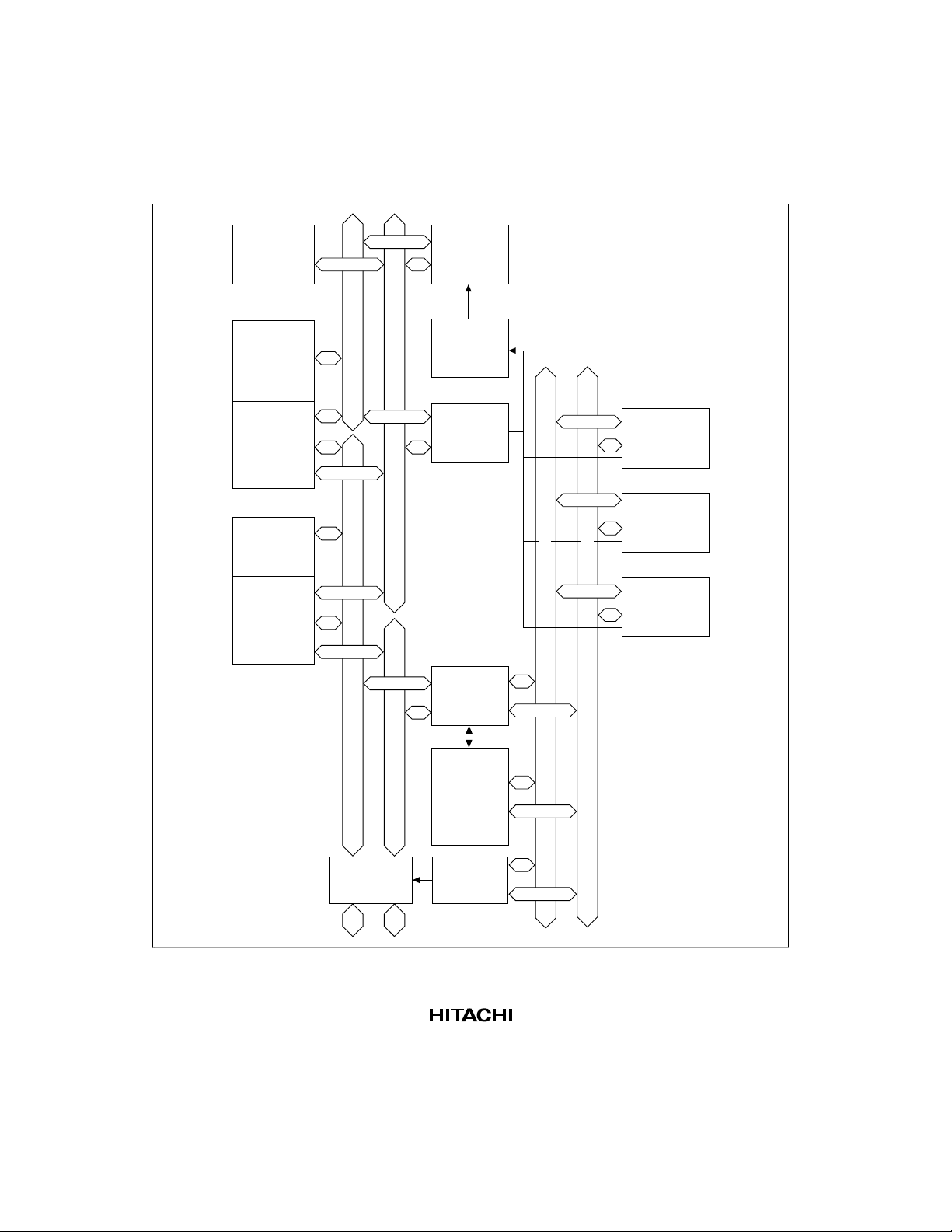
1.2 Block Diagram
Figure 1.1 shows a block diagram of the SH7708 Series.
Multiplier
MMU
(memory
management
unit)
Mixed
instruction/
data TLB
Cache
controller
Mixed
instruction/
data cache
memory
CPU
Interrupt
controller
32-bit data bus
32-bit virtual address bus
User break
controller
(2 channels)
Bus state
controller
SCI (serial
communication
interface)
Realtime
clock
Peripheral address bus
16-bit peripheral data bus
Timer
(3 channels)
PLL built-in
32-bit data bus
32-bit physical address bus
External bus
interface
clock
oscillator
WDT
(watchdog
timer)
I/O ports
Figure 1.1 SH7708 Series Block Diagram
6
Page 21
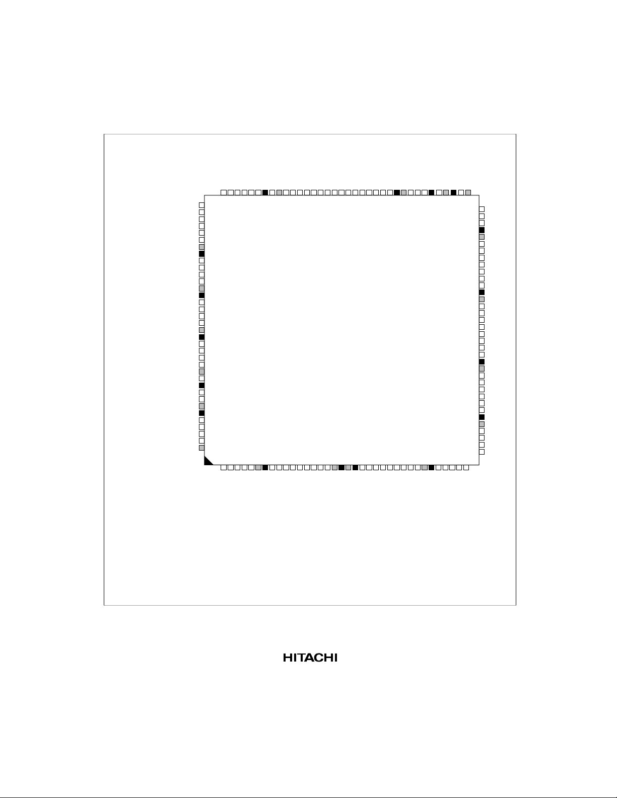
1.3 Pin Description
1.3.1 Pin Arrangement
CS6/CE1BRDRDWR
MD3/CE2A
MD4/CE2B
Vcc
CKIO
Vss
1
*
NC
STATUS0
STATUS1
BACK
IRQOUT
IOIS16
IRL0
IRL1
IRL2
IRL3
NMIBSRESET
BREQ
MD0/SCK
MD1/TXD
MD2/RXD
Vcc
Vss
4
*
XTAL
EXTAL
2
2
2
*
*
*
Vcc (PLL2)
CAP2
Vss (PLL2)
Vcc (PLL1)
2
*
CAP1
Vss (PLL1)
CS5/CE1A
CS4
CS3
CS2
CS1
CS0
Vss
WE3/DQMUU/ICIOWR
WE2/DQMUL/ICIORD
CASHH/CAS2H
CASHL/CAS2L
WE1/DQMLU
CASLL/CAS/OE
Vcc
Vss
Vcc
WE0/DQMLL
CASLH
Vss
Vcc
RAS/CE
MD5/RAS2
CKE
WAIT
Vss
TCLK
Vcc (RTC)
XTAL2
EXTAL2
Vss (RTC)
Vcc
D31
D30
D29
D28
Vss
100
90
120
SH7708(FP-144F)
SH7708S(TFP-144, FP-144F)
130
*2
*2
SH7708R(FP-144F)
Top view
140
144
1
D27
D26
D25
D24
Vss
Vcc
10
D15
D14
Vss
Vcc
Vss
20
Vcc
D13
D12
D11
D10
80
D9D8D7D6D5
30
D4D3D2D1D0
Vss
Vcc
70
60
50
40
A25
A24
A23
Vcc
Vss
A22
A21
A20
A19
A18
A17
A16
Vcc
Vss
A15
A14
A13
Vcc
Vss
A12
A11
A10
Vcc
Vss
A9
A8
A7
A6
A5
A4
Vcc
Vss
A3
A2
A1
A0
D17/Port1
D20/Port4
D19/Port3
D18/Port2
D16/Port0
Notes:
1.Make no connection.
D23/Port7
D22/Port6
D21/Port5
2.Power supply pins for the on-chip RTC and on-chip PLL. These pins must be
connected to the power supply even if the RTC or PLL are not used.
3.Power supply pins for the on-chip PLL. Except in hardware standby mode,
these pins must be connected to the power supply even if the PLL is not used.
4. SH7708:Vcc
SH7708S,SH7708R:CA
Figure 1.2 Pin Arrangement
7
Page 22

1.3.2 SH7708 Series Pin Functions
Table 1.2 SH7708 Series Pin Functions
No. Terminal I/O Description
1 D27 I/O Data bus
2 D26 I/O Data bus
3 D25 I/O Data bus
4 D24 I/O Data bus
5 D23/Port7 I/ O Data bus/port
6V
7V
SS
CC
8 D22/Port6 I/ O Data bus/port
9 D21/Port5 I/ O Data bus/port
10 D20/Port4 I/ O Data bus/port
11 D19/Port3 I/ O Data bus/port
12 D18/Port2 I/ O Data bus/port
13 D17/Port1 I/ O Data bus/port
14 D16/Port0 I/ O Data bus/port
15 D15 I/O Data bus
16 D14 I/O Data bus
17 V
18 V
19 V
20 V
SS
CC
SS
CC
21 D13 I/O Data bus
22 D12 I/O Data bus
23 D11 I/O Data bus
24 D10 I/O Data bus
25 D9 I/O Data bus
26 D8 I/O Data bus
27 D7 I/O Data bus
28 D6 I/O Data bus
29 D5 I/O Data bus
Power Power (0 V)
Power Power (3.3 V)
Power Power (0 V)
Power Power (3.3 V)
Power Power (0 V)
Power Power (3.3 V)
8
Page 23

Table 1.2 SH7708 Series Pin Functions (cont)
No. Terminal I/O Description
30 V
31 V
SS
CC
32 D4 I/O Data bus
33 D3 I/O Data bus
34 D2 I/O Data bus
35 D1 I/O Data bus
36 D0 I/O Data bus
37 A0 O Address bus
38 A1 O Address bus
39 A2 O Address bus
40 A3 O Address bus
41 V
42 V
SS
CC
43 A4 O Address bus
44 A5 O Address bus
45 A6 O Address bus
46 A7 O Address bus
47 A8 O Address bus
48 A9 O Address bus
49 V
50 V
SS
CC
51 A10 O Address bus
52 A11 O Address bus
53 A12 O Address bus
54 V
55 V
SS
CC
56 A13 O Address bus
57 A14 O Address bus
58 A15 O Address bus
59 V
60 V
SS
CC
Power Power (0 V)
Power Power (3.3 V)
Power Power (0 V)
Power Power (3.3 V)
Power Power (0 V)
Power Power (3.3 V)
Power Power (0 V)
Power Power (3.3 V)
Power Power (0 V)
Power Power (3.3 V)
9
Page 24

Table 1.2 SH7708 Series Pin Functions (cont)
No. Terminal I/O Description
61 A16 O Address bus
62 A17 O Address bus
63 A18 O Address bus
64 A19 O Address bus
65 A20 O Address bus
66 A21 O Address bus
67 A22 O Address bus
68 V
69 V
SS
CC
70 A23 O Address bus
71 A24 O Address bus
72 A25 O Address bus
73 VSS(PLL1)*
2
74 CAP1 O External capacitance pin for PLL1
75 VCC(PLL1)*
76 VSS(PLL2)*
2
2
77 CAP2 O External capacitance pin for PLL2
78 VCC(PLL2)*
2
79 EXTAL I External clock/crystal oscillator pin
80 XTAL O Crystal oscillator pin
81(SH7708) V
81(SH7708S,
CC
CA I Chip active
SH7708R)
82 V
83 V
SS
CC
84 MD2/RXD I Operating mode pin/serial data input
85 MD1/TXD I/O Operating mode pin/serial data output
86 MD0/SCK I/O Operating mode pin/serial clock
87 BREQ I Bus request
88 RESET I Reset
89 NMI I Nonmaskable interrupt request
90 IRL3 I External interrupt source input
Power Power (0 V)
Power Power (3.3 V)
Power Power (0 V) for PLL1
Power Power (3.3 V) for PLL1
Power Power (0 V) for PLL2
Power Power (3.3 V) for PLL2
Power Power(3.3V)
Power Power (0 V)
Power Power (3.3 V)
10
Page 25

Table 1.2 SH7708 Series Pin Functions (cont)
No. Terminal I/O Description
91 IRL2 I External interrupt source input
92 IRL1 I External interrupt source input
93 IRL0 I External interrupt source input
94 IOIS16 I IO16-bit instruction
95 IRQOUT O Bus request notification output
96 BACK O Bus acknowledge
97 STATUS1 O Processor status
98 STATUS0 O Processor status
99 NC O Leave unconnected
100 V
SS
101 CKIO I /O System clock I/O
102 V
CC
103 MD4/CE2B I/O Operating mode pin/PCMCIA CE pin
104 MD3/CE2A I/O Operating mode pin/PCMCIA CE pin
105 BS O Bus cycle start
106 RD/WR O Read/write
107 RD O Read pulse
108 CS6/CE1B O Chip select 6/PCMCIA CE pin
109 CS5/CE1A O Chip select 5/PCMCIA CE pin
110 CS4 O Chip select 4
111 CS3 O Chip select 3
112 CS2 O Chip select 2
113 CS1 O Chip select 1
114 CS0 O Chip select 0
115 V
116 V
SS
CC
117 WE3/DQMUU/ICIOWR O D31–D24 selection signal/IO write
118 WE2/DQMUL/ICIORD O D23–D16 selection signal/IO read
119 CASHH/CAS2H O D31–D24/D15–D8 selection signal
120 CASHL/CAS2L O D23–D16/D7–D0 selection signal
121 V
SS
Power Power (0 V)
Power Power (3.3 V)
Power Power (0 V)
Power Power (3.3 V)
Power Power (0 V)
11
Page 26

Table 1.2 SH7708 Series Pin Functions (cont)
No. Terminal I/O Description
122 V
CC
123 WE1/DQMLU O D15–D8 selection signal
124 WE0/DQMLL O D7–D0 selection signal
125 CASLH O D15–D8 selection signal
126 CASLL/CAS/OE O D7–D0 selection/memory selection signal
127 V
128 V
SS
CC
129 RAS/CE O RAS for DRAM, SDRAM/CE for PSRAM
130 MD5/RAS2 I/O Operating mode pin/RAS for DRAM
131 CKE O Clock enable control for SDRAM
132 WAIT I Hardware wait request
133 V
SS
134 TCLK I/O Clock I/O for TMU/RTC
135 VCC (RTC)*
3
136 XTAL2 O Crystal oscillator pin for on-chip RTC
137 EXTAL2 I Crystal oscillator pin for on-chip RTC
138 VSS (RTC)*
139 V
CC
3
140 D31 I/O Data bus
141 D30 I/O Data bus
142 D29 I/O Data bus
143 D28 I/O Data bus
144 V
SS
Notes: 1. Except in hardware standby mode, connect all VCC and VSS pins to the system power
supply (power should be supplied constantly). In hardware standby mode, power should
be supplied at least to V
pins other than VCC (RTC) and VSS (RTC), hold the CA pin low.
2. Power should be supplied regardless of whether or not the on-chip PLL is used.
3. Power should be supplied regardless of whether or not the RTC is used.
Power Power (3.3 V)
Power Power (0 V)
Power Power (3.3 V)
Power Power (0 V)
Power Power (3.3 V)
Power Power (0 V)
Power Power (3.3 V)
Power Power (0 V)
(RTC) and VSS (RTC). If power is not supplied to VCC and V
CC
SS
12
Page 27

Section 2 CPU
2.1 Register Configuration
2.1.1 Privileged Mode and Banks
Processor Modes: There are two processor modes: user mode and privileged mode. The
SH7708 Series normally operates in user mode, and enters privileged mode when an exception
occurs or an interrupt is accepted. There are three kinds of registers—general registers, system
registers, and control registers—and the registers that can be accessed differ in the two processor
modes.
General Registers: There are 16 general registers, designated R0 to R15. General registers R0
to R7 are banked registers which are switched by a processor mode change. In privileged mode, the
register bank bit (RB) in the status register (SR) defines which banked register set is accessed as
general registers, and which set is accessed only through the load control register (LDC) and store
control register (STC) instructions.
When the RB bit is 1, BANK1 general registers R0_BANK1–R7_BANK1 and non-banked general
registers R8–R15 function as the general register set, with BANK0 general registers R0_BANK0–
R7_BANK0 accessed only by the LDC/STC instructions.
When the RB bit is 0, BANK0 general registers R0_BANK0–R7_BANK0 and nonbanked general
registers R8–R15 function as the general register set, with BANK1 general registers R0_BANK1–
R7_BANK1 accessed only by the LDC/STC instructions. In user mode, the 16 registers
comprising bank 0 general registers R0_BANK0–R7_BANK0 and non-banked registers R8–R15
can be accessed as general registers R0–R15, and bank 1 general registers R0_BANK1–
R7_BANK1 cannot be accessed.
Control Registers: Control registers comprise the global base register (GBR) and status
register (SR) which can be accessed in both processor modes, and the saved status register (SSR),
saved program counter (SPC), and vector base register (VBR) which can only be accessed in
privileged mode. Some bits of the status register (such as the RB bit) can only be accessed in
privileged mode.
System Registers: System registers comprise the multiply and accumulate registers
(MACL/MACH), the procedure register (PR), and the program counter (PC). Access to these
registers does not depend on the processor mode.
The register configuration in each mode is shown in figures 2.1 and 2.2.
Switching between user mode and privileged mode is controlled by the processor mode bit (MD) in
the status register.
13
Page 28
31 0
R0_BANK0*
R1_BANK0*
R2_BANK0*
R3_BANK0*
R4_BANK0*
R5_BANK0*
R6_BANK0*
R7_BANK0*
1, *2
2
2
2
2
2
2
2
R8
R9
R10
R11
R12
R13
R14
R15
SR
GBR
MACH
MACL
PR
PC
User mode register configuration
14
Notes: 1.
R0 functions as an index register in the indexed register-indirect addressing
mode and indexed GBR-indirect addressing mode.
2.
Banked register
Figure 2.1 User Mode Register Configuration
Page 29
31 0
R0_BANK1*
R1_BANK1*
R2_BANK1*
R3_BANK1*
R4_BANK1*
R5_BANK1*
R6_BANK1*
R7_BANK1*
1, *2
2
2
2
2
2
2
2
R8
R9
R10
R11
R12
R13
R14
R15
31 0
R0_BANK0*
R1_BANK0*
R2_BANK0*
R3_BANK0*
R4_BANK0*
R5_BANK0*
R6_BANK0*
R7_BANK0*
1, *3
3
3
3
3
3
3
3
R8
R9
R10
R11
R12
R13
R14
R15
SR
SSR
GBR
MACH
MACL
PR
VBR
PC
SPC
R0_BANK0*
R1_BANK0*
R2_BANK0*
R3_BANK0*
R4_BANK0*
R5_BANK0*
R6_BANK0*
R7_BANK0*
1, *3
3
3
3
3
3
3
3
a. Privileged mode
register configuration
(RB = 1)
SR
SSR
GBR
MACH
MACL
PR
VBR
PC
SPC
R0_BANK1*
R1_BANK1*
R2_BANK1*
R3_BANK1*
R4_BANK1*
R5_BANK1*
1, *2
2
2
2
2
2
R6_BANK1*2
R7_BANK1*
2
b. Privileged mode
register configuration
(RB = 0)
Notes:
R0 functions as an index
1.
register in the indexed
register-indirect addressing
mode and indexed GBR-
indirect addressing mode.
Banked register
2.
When the RB bit of the SR
register is 1, the register can
be accessed for general use.
When the RB bit is 0, it can
only be accessed with the
LDC/STC instruction.
Banked register
3.
When the RB bit of the SR
register is 0, the register can
be accessed for general use.
When the RB bit is 1, it can
only be accessed with the
LDC/STC instruction.
Figure 2.2 Privileged Mode Register Configuration
15
Page 30
Register values after a reset are shown in table 2.1.
Table 2.1 Initial Register Values
Type Registers Initial Value
General registers R0 to R15 Undefined
Control registers SR MD bit = 1, RB bit = 1, BL bit = 1, I3–
I0 = 1111 (H'F), reserved bits = 0,
others undefined
GBR, SSR, SPC Undefined
VBR H'00000000
System registers MACH, MACL, PR Undefined
PC H'A0000000
Note: Initialized by a power-on reset or manual reset.
2.1.2 General Registers
There are 16 general registers, designated R0 to R15 (figure 2.3). General registers R0 to R7 are
banked registers, with a different R0–R7 register bank (R0_BANK0–R7_BANK0 or R0_BANK1–
R7_BANK1) being accessed according to the processor mode. For details, see section 2.1.1,
Privileged Mode and Banks.
31 0
1, *2
R0*
2
R1*
2
R2*
2
R3*
2
R4*
2
R5*
2
R6*
2
R7*
R8
R9
R10
R11
R12
R13
R14
R15
16
General Registers
Notes:
1.
R0 functions as an index register in the indexed
register-indirect addressing mode and indexed
GBR-indirect addressing mode. In some instructions,
only R0 can be used as the source register or
destination register.
2.
R0–R7 are banked registers.
In privileged mode, SR.RB specifies which banked
registers are accessed as general registers
(R0_BANK0–R7_BANK0 or R0_BANK1–R7_BANK1).
Figure 2.3 General Registers
Page 31

2.1.3 System Registers
System registers can be accessed by the LDS and STS instructions. When an exception occurs, the
contents of the program counter (PC) are saved in the saved program counter (SPC). The SPC
contents are restored to the PC by the RTE instruction used at the end of the exception handling.
There are four system registers, as follows.
• Multiply and accumulate high register (MACH)
• Multiply and accumulate low register (MACL)
• Procedure register (PR)
• Program counter (PC)
The system register configuration is shown in figure 2.4.
31 0
MACH
MACL
31 0
PR
31 0
PC
System Registers
Multiply and Accumulate High and Low Registers
(MACH/L)
Store the results of multiply-and-accumulate operations.
Its contents are undefined after a reset.
Procedure Register (PR)
Stores the return address for exiting a subroutine
procedure.
Its contents are undefined after a reset.
Program Counter (PC)
Indicates the address four addresses (two instructions)
ahead of the currently executing instruction. Initialized
to H'A0000000 by a reset.
Figure 2.4 System Registers
2.1.4 Control Registers
Control registers can be accessed in privileged mode using the LDC and STC instructions. The
GBR register can also be accessed in user mode. There are five control registers, as follows:
• Status register (SR)
• Saved status register (SSR)
• Saved program counter (SPC)
• Global base register (GBR)
• Vector base register (VBR)
17
Page 32

31 0
SSR
Saved Status Register (SSR)
Stores current SR value at time of exception to indicate processor
status in return to instruction stream from exception handler.
Its contents are undefined after a reset.
31 0
SPC
31 0
GBR
31 0
VBR
31 29 28 27 10 9 8 7 01 3
30
0RB
MD BL M Q0––––––––––––––––––––––––––––0 I3 I2 I1 I0 0 0 S T
MD:
Processor operation mode bit: Indicates the processor operation mode as follows:
MD =1: Privileged mode; MD = 0: User mode
MD is set to 1 on generation of an exception or interrupt , and is initialized to 1 by a reset.
RB:
Register bank bit: Determines the bank of general registers R0–R7 used in processing mode.
RB = 1: R0_BANK1–R7_BANK1 and R8–R15 are general registers, and R0_BANK0–
R7_BANK0 can be accessed by LDC/STC instructions.
RB = 0: R0_BANK0–R7_BANK0 and R8–R15 are general registers, and R0_BANK1–
R7_BANK1 can be accessed by LDC/STC instructions.
RB is set to 1 on generation of an exception or interrupt , and is initialized to 1 by a reset.
BL:
Block bit
BL = 1: Exceptions and interrupts are suppressed. See section 4, Exception
Handling, for details.
BL = 0: Exceptions and interrupts are accepted.
M and Q bits:
I3–I0 bits:
Note:
BL is set to 1 on generation of an exception or interrupt , and is initialized to 1 by a reset.
Used by the DIV0S/U and DIV1 instructions.
Interrupt mask bits: 4-bit field indicating the interrupt request mask level.
I3–I0 do not change to the interrupt acceptance level when an interrupt is generated.
Initialized to B'1111 by a reset.
S bit:
Used by the MAC instruction.
T bit:
Used by the MOVT, CMP/cond, TAS, TST, BT, BF, SETT, CLRT, and DT instructions to
indicate true (1) or false (0).
Used by the ADDV/C, SUBV/C, DIV0U/S, DIV1, NEGC, SHAR/L, SHLR/L, ROTR/L, and
ROTCR/L instructions to indicate a carry, borrow, overflow, or underflow.
0 bits:
These bits always read 0, and the write value should always be 0.
The M, Q, S, and T bits can be set or cleared by special instructions in user mode.
Their values are undefined after a reset. All other bits can be read or written in privileged mode.
Saved Program Counter (SPC)
Stores current PC value at time of exception to indicate return
address at completion of exception handling.
Its contents are undefined after a reset.
Global Base Register (GBR)
Stores base address of GBR-indirect addressing mode.
The GBR-indirect addressing mode is used for on-chip supporting
module register area data transfers and logic operations.
The GBR register can also be accessed in user mode.
Its contents are undefined after a reset.
Vector Base Register (VBR)
Stores base address of exception handling vector area.
Initialized to H'0000000 by a reset.
Status
register
(SR)
18
Figure 2.5 Register Set Overview, Control Registers
Page 33

2 . 2 Data Formats
2.2.1 Data Format in Registers
Register operands are always longwords (32 bits, figure 2.6). When a memory operand is only a
byte (8 bits) or a word (16 bits), it is sign-extended into a longword when loaded into a register.
31 0
Longword
Figure 2.6 Longword
2.2.2 Data Format in Memory
Memory data formats are classified into bytes, words, and longwords. Memory can be accessed in
8-bit byte, 16-bit word, or 32-bit longword form. A memory operand less than 32 bits in length is
sign-extended before being stored in a register.
A word operand must be accessed starting from a word boundary (even address of a 2-byte unit:
address 2n), and a longword operand starting from a longword boundary (even address of a 4-byte
unit: address 4n). An address error will result if this rule is not observed. A byte operand can be
accessed from any address.
Big-endian or little-endian byte order can be selected for the data format. The endian mode should be
set with the MD5 external pin in a power-on reset. Big-endian mode is selected when the MD5 pin
is low, and little-endian when high. The endian mode cannot be changed dynamically. Bit positions
are numbered left to right from most-significant to least-significant. Thus, in a 32-bit longword,
the leftmost bit, bit 31, is the most significant bit and the rightmost bit, bit 0, is the least
significant bit.
The data format in memory is shown in figure 2.7. In little-endian mode, data written in byte-size
(8-bit) units should be read in byte-size units, and data written in word-size (16-bit) units should be
read in word-size units.
19
Page 34

Address A
Address A + 4
Address A + 8
Address A + 1 Address A + 3
Address A
23 7
31 015
Byte0 Byte1 Byte2 Byte3
Word0
Longword Longword
Word1
Address A + 10 Address A + 8
Address A + 11
31 015
Byte3 Byte2 Byte1 Byte0
Word1
Address A + 9Address A + 2
23 7
Word0
Address A + 8
Address A + 4
Address A
Big-endian mode
Little-endian mode
Figure 2.7 Byte, Word, and Longword Alignment
2.3 Instruction Features
2.3.1 Execution Environment
Data Length: The SH7708 Series instruction set is implemented with fixed-length 16-bit wide
instructions executed in a pipelined sequence with single-cycle execution for most instructions. All
operations are executed in 32-bit longword units. Memory can be accessed in 8-bit byte, 16-bit
word, or 32-bit longword units, with byte or word units sign-extended into 32-bit longwords.
Literals are sign-extended in arithmetic operations (MOV, ADD, and CMP/EQ instructions) and
zero-extended in logical operations (TST, AND, OR, and XOR instructions).
Load/Store Architecture: The SH7708 Series features a load-store architecture in which basic
operations are executed in registers. Operations requiring memory access are executed in registers
following register loading, except for bit-manipulation operations such as logical AND functions,
which are executed directly in memory.
Delayed Branching: Unconditional branching is implemented as delayed branch operations.
Pipeline disruptions due to branching are minimized by the execution of the instruction following
the delayed branch instruction prior to branching. Conditional branch instructions are of two kinds,
delayed and normal.
BRA TRGET
ADD R1, R0 ;ADD is executed prior to branching to TRGET
20
Page 35

T bit: The T bit in the status register (SR) is used to indicate the result of compare operations,
and is read as a TRUE/FALSE condition determining if a conditional branch is taken or not. To
improve processing speed, the T bit logic state is modified only by specific operations. An
example of how the T bit may be used in a sequence of operations is shown below.
ADD #1, R0 ;T bit not modified by ADD operation
CMP/EQ R1, R0 ;T bit set to 1 when R0 = 0
BT TRGET ;branch taken to TRGET when T bit = 1 (R0 = 0)
Literals: Byte-length literals are inserted directly into the instruction code as immediate data. To
maintain the 16-bit fixed-length instruction code, word or longword literals are stored in a table in
main memory rather than inserted directly into the instruction code. The memory table is accessed
by the MOV instruction using PC-relative addressing with displacement, as follows:
MOV.W @(disp, PC), R0
Absolute Addresses: As with word and longword literals, absolute addresses must also be
stored in a table in main memory. The value of the absolute address is transferred to a register and
the operand access is specified by indexed register-indirect addressing, with the absolute address
loaded (like word and longword immediate data) during instruction execution.
16-Bit and 32-Bit Displacements: In the same way, 16-bit and 32-bit displacements also
must be stored in a table in main memory. Exactly like absolute addresses, the displacement value
is transferred to a register and the operand access is specified by indexed register-indirect addressing,
loading the displacement (like word and longword immediate data) during instruction execution.
21
Page 36

2.3.2 Addressing Modes
Addressing modes and effective address calculation methods are shown in table 2.2.
Table 2.2 Addressing Modes and Effective Addresses
Addressing
Mode
Register direct Rn Effective address is register Rn. (Operand is
Register
indirect
Register
indirect with
post-increment
Register
indirect with
pre-decrement
Instructio
n Format Effective Address Calculation MethodCalculation Formula
register Rn contents.)
@Rn Effective address is register Rn contents.
Rn Rn
@Rn+ Effective address is register Rn contents. A
constant is added to Rn after instruction
execution: 1 for a byte operand, 2 for a word
operand, 4 for a longword operand.
Rn
Rn + 1/2/4
1/2/4
@–Rn Effective address is register Rn contents,
decremented by a constant beforehand: 1 for
a byte operand, 2 for a word operand, 4 for a
longword operand.
Rn
Rn – 1/2/4
+
–
Rn
Rn – 1/2/4
—
Rn
Rn
After instruction
execution
Byte: Rn + 1 → Rn
Word: Rn + 2 → Rn
Longword: Rn + 4 → Rn
Byte: Rn – 1 → Rn
Word: Rn – 2 → Rn
Longword: Rn – 4 → Rn
(Instruction executed
with Rn after
calculation)
22
1/2/4
Page 37

Table 2.2 Addressing Modes and Effective Addresses (cont)
Addressing
Mode
Register
indirect with
displacement
Indexed
register indirect
GBR indirect
with
displacement
Instructio
n Format Effective Address Calculation MethodCalculation Formula
@(disp:4,
Rn)
@(R0, Rn) Effective address is sum of register Rn and
Effective address is register Rn contents
with 4-bit displacement disp added. After
disp is zero-extended, it is multiplied by 1
(byte), 2 (word), or 4 (longword), according to
the operand size.
Rn
disp
(zero-extended)
1/2/4
+
×
Rn
+ disp × 1/2/4
Byte: Rn + disp
Word: Rn + disp × 2
Longword:
Rn + disp × 4
Rn + R0
R0 contents.
Rn
+
Rn + R0
R0
@(disp:8,
GBR)
Effective address is register GBR contents
with 8-bit displacement disp added. After
disp is zero-extended, it is multiplied by 1
(byte), 2 (word), or 4 (longword), according to
the operand size.
Byte: GBR + disp
Word: GBR + disp × 2
Longword:
GBR + disp × 4
Indexed GBR
indirect
GBR
disp
(zero-extended)
1/2/4
+
×
GBR
+ disp × 1/2/4
@(R0, GBR)Effective address is sum of register GBR and
R0 contents.
GBR
+
GBR + R0
R0
GBR + R0
23
Page 38

Table 2.2 Addressing Modes and Effective Addresses (cont)
Addressing
Mode
PC-relative
with
displacement
Instructio
n Format Effective Address Calculation MethodCalculation Formula
@(disp:8,
PC)
Effective address is register PC contents
with 8-bit displacement disp added. After
disp is zero-extended, it is multiplied by 2
(word), or 4 (longword), according to the
operand size. With a longword operand, the
lower 2 bits of PC are masked.
PC
(for longword)
&
H'FFFFFFFC
+
disp
(zero-extended)
x
2/4
PC + disp × 2
or
PC&H'FFFFFFFC
+ disp × 4
PC-relative disp:8 Effective address is register PC contents
with 8-bit displacement disp added after
being sign-extended and multiplied by 2.
PC
disp
+
PC + disp × 2
(sign-extended)
×
Word: PC + disp × 2
Longword:
PC & H'FFFF FFFC +
disp × 4
PC + disp × 2
24
2
disp:12 Effective address is register PC contents
with 12-bit displacement disp added after
being sign-extended and multiplied by 2.
PC
disp
(sign-extended)
2
+
PC + disp × 2
×
PC + disp × 2
Page 39

Table 2.2 Addressing Modes and Effective Addresses (cont)
Addressing
Mode
PC-relative Rn Effective address is sum of register PC and
Immediate #imm:8 8-bit immediate data imm of TST, AND, OR, or
Note: For the addressing modes below that use a displacement (disp), the assembler descriptions
in this manual show the value before scaling (x1, x2, or x4) is performed according to the
operand size. This is done to clarify the operation of the IC. Refer to the relevant assembler
notation rules for the actual assembler descriptions.
@ (disp:4, Rn) ; Register indirect with displacement
@ (disp:8, Rn) ; GBR indirect with displacement
@ (disp:8, PC) ; PC-relative with displacement
disp:8, disp:12; PC-relative
Instructio
n Format Effective Address Calculation MethodCalculation Formula
PC + Rn
Rn contents.
PC
+
Rn
XOR instruction is zero-extended.
#imm:8 8-bit immediate data imm of MOV, ADD, or
CMP/EQ instruction is sign-extended.
#imm:8 8-bit immediate data imm of TRAPA
instruction is zero-extended and multiplied
by 4.
PC + Rn
—
—
—
25
Page 40

2.3.3 Instruction Formats
Table 2.3 explains the meaning of instruction formats and source and destination operands. The
meaning of the operands depends on the operation code. The following symbols are used.
xxxx: Operation code
mmmm: Source register
nnnn: Destination register
iiii: Immediate data
dddd: Displacement
Table 2.3 Instruction Formats
Instruction Format
0 format
n format
m format
15 0
xxxx xxxx xxxxxxxx
15 0
xxxx xxxx xxxxnnnn
15 0
mmmm
xxxx xxxx
xxxx
Source
Operand
— — NOP
— nnnn: register
Control register or
system register
Control register or
system register
mmmm: register
direct
mmmm: register
indirect with postincrement
mmmm: register
indirect
mmmm: PCrelative using Rm
Destination
Operand
direct
nnnn: register
direct
nnnn: register
indirect with
pre-decrement
Control register
or system
register
Control register
or system
register
— JMP @Rm
— BRAF R m
Instruction
Example
MOVT Rn
STS
MACH,Rn
STC.L
SR,@–Rn
LDC
Rm,SR
LDC.L
@Rm+,SR
26
Page 41

Table 2.3 Instruction Formats (cont)
Instruction Format
nm format
md format
nd4 format
15 0
xxxx xxxx
15 0
xxxx dddd
15 0
xxxx
nnnn
xxxx
xxxx
mmmm
mmmm
nnnn
dddd
Source
Operand
mmmm: register
direct
mmmm: register
direct
mmmm: register
indirect with postincrement
(multiply-andaccumulate
operation)
nnnn: * register
indirect with postincrement
(multiply-andaccumulate
operation)
mmmm: register
indirect with postincrement
mmmm: register
direct
mmmm: register
direct
mmmmdddd:
register indirect
with displacement
R0 (register
direct)
Destination
Operand
nnnn: register
direct
nnnn: register
indirect
MACH,MACL MAC.W
nnnn: register
direct
nnnn: register
indirect with
pre-decrement
nnnn: indexed
register indirect
R0 (register
direct)
nnnndddd:
register indirect
with
displacement
Instruction
Example
ADD Rm,Rn
MOV.L
Rm,@Rn
@Rm+,@Rn+
MOV.L
@Rm+,Rn
MOV.L
Rm,@–Rn
MOV.L
Rm,@(R0,Rn)
MOV.B
@(disp,Rm),R0
MOV.B
R0,@(disp,Rn)
27
Page 42

Table 2.3 Instruction Formats (cont)
Instruction Format
nmd format
d format
d12 format
nd8 format
i format
ni format
15 0
xxxx dddd
15 0
xxxx
15 0
xxxx
15 0
xxxx
15 0
xxxx
15 0
xxxx
nnnn
xxxx
dddd
nnnn
xxxx
nnnn
mmmm
dddd
dddd dddd
dddd
i i i i
i i i i
dddd
dddd
i i i i
i i i i
Source
Operand
mmmm: register
direct
mmmmdddd:
register indirect
with displacement
dddddddd: GBR
indirect with
displacement
R0 (register
direct)
dddddddd:
PC-relative with
displacement
dddddddd:
PC-relative
dddddddddddd:
PC-relative
dddddddd:
PC-relative with
displacement
iiiiiiii: immediate Indexed GBR
iiiiiiii: immediate R0 (register
iiiiiiii: immediate — TRAPA #imm
iiiiiiii: immediate nnnn: register
Destination
Operand
nnnndddd:
register
indirect with
displacement
nnnn: register
direct
R0 (register
direct)
dddddddd:
GBR indirect
with
displacement
R0 (register
direct)
— BF label
— BRA label
nnnn: register
direct
indirect
direct)
direct
Instruction
Example
MOV.L
Rm,@(disp,Rn)
MOV.L
@(disp,Rm),Rn
MOV.L
@(disp,GBR),R0
MOV.L
R0,@(disp,GBR)
MOVA
@(disp,PC),R0
(label = disp +
PC)
MOV.L
@(disp,PC),Rn
AND.B
#imm,
@(R0,GBR)
AND
#imm,R0
ADD
#imm,Rn
Note: In a multiply-and-accumulate instruction, nnnn is the source register.
28
Page 43

2. 4 Instruction Set
2.4.1 Instruction Set Classified by Function
The SH7708 Series instruction set includes 68 basic instruction types, as listed in table 2.4.
Table 2.4 Classification of Instructions
Operatio
ClassificationTypes
Data transfer 5 MOV Data transfer 39
Arithmetic 21 ADD Binary addition 33
operations
n Code Function
MOVA Effective address transfer
MOVT T bit transfer
SWAP Swap of upper and lower bytes
XTRCT Extraction of middle of linked registers
ADDC Binary addition with carry
ADDV Binary addition with overflow check
CMP/cond Comparison
DIV1 Division
DIV0S Initialization of signed division
DIV0U Initialization of unsigned division
DMULS Signed double-precision multiplication
DMULU Unsigned double-precision multiplication
DT Decrement and test
EXTS Sign extension
EXTU Zero extension
MAC Multiply-and-accumulate operation,
double-precision multiply-and-accumulate
operation
No. of
Instructio
ns
29
Page 44

Table 2.4 Classification of Instructions (cont)
Operatio
ClassificationTypes
Arithmetic 21 MUL Double-precision multiplication 33
operations
(cont)
Logic 6 AND Logical AND 14
operations
Shift 12 ROTL One-bit left rotation 16
n Code Function
MULS Signed multiplication
MULU Unsigned multiplication
NEG Negation
NEGC Negation with borrow
SUB Binary subtraction
SUBC Binary subtraction with borrow
SUBV Binary subtraction with underflow check
NOT Bit inversion
OR Logical OR
TAS Memory test and bit set
TST Logical AND and T bit set
XOR Exclusive OR
ROTR One-bit right rotation
ROTCL One-bit left rotation with T bit
ROTCR One-bit right rotation with T bit
SHAL One-bit arithmetic left shift
SHAR One-bit arithmetic right shift
SHLL One-bit logical left shift
SHLLn n-bit logical left shift
SHLR One-bit logical right shift
SHLRn n-bit logical right shift
SHAD Dynamic arithmetic shift
SHLD Dynamic logical shift
No. of
Instructio
ns
30
Page 45

Table 2.4 Classification of Instructions (cont)
Operatio
ClassificationType
s
Branch 9 BF Conditional branch, delayed conditional
System 15 CLRT T bit clear 75
control
Total: 68 188
n Code Function
branch (T = 0)
BT Conditional branch, delayed conditional
branch (T = 1)
BRA Unconditional branch
BRAF Unconditional branch
BSR Branch to subroutine procedure
BSRF Branch to subroutine procedure
JMP Unconditional branch
JSR Branch to subroutine procedure
RTS Return from subroutine procedure
CLRMAC MAC register clear
CLRS Clear S bit
LDC Load to control register
LDS Load to system register
LDTLB Load PTE to TLB
NOP No operation
PREF Prefetch data to cache
RTE Return from exception handling
SETS Set S bit
SETT Set T bit
SLEEP Shift to power-down mode
STC Store from control register
STS Store from system register
TRAPA Trap exception handling
No. of
Instructio
ns
11
Table 2.5 lists the SH7708 Series instruction code formats.
31
Page 46

Table 2.5 Instruction Code Format
Item Format Explanation
Instruction
mnemonic
Instruction
code
Operation →, ←
Privileged
mode
Execution
cycles
T bit Value of T bit after instruction is executed
Note: Scaling (×1, ×2, ×4) is performed according to the instruction operand size.
OP.Sz SRC,DEST OP: Operation code
Sz: Size
SRC: Source
DEST: Destination
Rm: Source register
Rn: Destination register
imm: Immediate data
disp: Displacement
MSB ↔ LSB mmmm: Source register
nnnn: Destination register
0000: R0
0001: R1
...........
1111: R15
iiii: Immediate data
dddd: Displacement
Direction of transfer
(xx)
M/Q/T
&
|
∧
~
<<n, >>n
Memory operand
Flag bits in SR
Logical AND of each bit
Logical OR of each bit
Exclusive OR of each bit
Logical NOT of each bit
n-bit shift
Indicates whether privileged mode applies
Value when no wait states are inserted
The execution cycles listed in the table are minimums. The
actual number of cycles may be increased in cases such
as the following:
1. When contention occurs between instruction fetches
and data access
2. When the destination register of the load instruction
(memory → register) and the register used by the next
instruction are the same
—: No change
32
Page 47

Table 2.6 lists the SH7708 Series data transfer instructions
Table 2.6 Data Transfer Instructions
Privileged
Instruction Operation Code
MOV #imm,Rn imm → Sign extension
→ Rn
MOV.W @(disp,PC),Rn (disp × 2 + PC) → Sign
extension → Rn
MOV.L @(disp,PC),Rn (disp × 4 + PC) → Rn 1101nnnndddddddd —1—
MOV Rm,Rn Rm → Rn 0110nnnnmmmm0011 —1—
MOV.B Rm,@Rn Rm → (Rn) 0010nnnnmmmm0000 —1—
MOV.W Rm,@Rn Rm → (Rn) 0010nnnnmmmm0001 —1—
MOV.L Rm,@Rn Rm → (Rn) 0010nnnnmmmm0010 —1—
MOV.B @Rm,Rn (Rm) → Sign extension
→ Rn
MOV.W @Rm,Rn (Rm) → Sign extension
→ Rn
MOV.L @Rm,Rn (Rm) → Rn 0110nnnnmmmm0010 —1—
MOV.B Rm,@–Rn Rn–1 → Rn, Rm → (Rn) 0010nnnnmmmm0100 —1—
MOV.W Rm,@–Rn Rn–2 → Rn, Rm → (Rn) 0010nnnnmmmm0101 —1—
MOV.L Rm,@–Rn Rn–4 → Rn, Rm → (Rn) 0010nnnnmmmm0110 —1—
MOV.B @Rm+,Rn (Rm) → Sign extension
→ Rn, Rm + 1 → Rm
MOV.W @Rm+,Rn (Rm) → Sign extension
→ Rn, Rm + 2 → Rm
MOV.L @Rm+,Rn (Rm) → Rn,Rm + 4 → Rm 0110nnnnmmmm0110 —1—
MOV.B R0,@(disp,Rn) R0 → (disp + Rn) 10000000nnnndddd —1—
MOV.W R0,@(disp,Rn) R0 → (disp × 2 + Rn) 10000001nnnndddd —1—
MOV.L Rm,@(disp,Rn) Rm → (disp × 4 + Rn) 0001nnnnmmmmdddd —1—
MOV.B @(disp,Rm),R0 (disp + Rm) → Sign
extension → R0
MOV.W @(disp,Rm),R0 (disp × 2 + Rm) → Sign
extension → R0
MOV.L @(disp,Rm),Rn (disp × 4 + Rm) → Rn 0101nnnnmmmmdddd —1—
MOV.B Rm,@(R0,Rn) Rm → (R0 + Rn) 0000nnnnmmmm0100 —1—
MOV.W Rm,@(R0,Rn) Rm → (R0 + Rn) 0000nnnnmmmm0101 —1—
1110nnnniiiiiiii —1—
1001nnnndddddddd —1—
0110nnnnmmmm0000 —1—
0110nnnnmmmm0001 —1—
0110nnnnmmmm0100 —1—
0110nnnnmmmm0101 —1—
10000100mmmmdddd —1—
10000101mmmmdddd —1—
Mode Cycles T Bit
33
Page 48

Table 2.6 Data Transfer Instructions (cont)
Privileged
Instruction Operation Code
MOV.L Rm,@(R0,Rn) Rm → (R0 + Rn) 0000nnnnmmmm0110 —1—
MOV.B @(R0,Rm),Rn (R0 + Rm) → Sign extension
→ Rn
MOV.W @(R0,Rm),Rn (R0 + Rm) → Sign extension
→ Rn
MOV.L @(R0,Rm),Rn (R0 + Rm) → Rn 0000nnnnmmmm1110 —1—
MOV.B R0,@(disp,GBR) R0 → (disp + GBR) 11000000dddddddd —1—
MOV.W R0,@(disp,GBR) R0 → (disp ×2 + GBR) 11000001dddddddd —1—
MOV.L R0,@(disp,GBR) R0 → (disp × 4 + GBR) 11000010dddddddd —1—
MOV.B @(disp,GBR),R0 (disp + GBR) → Sign
extension → R0
MOV.W @(disp,GBR),R0 (disp × 2 + GBR) →
Sign extension → R0
MOV.L @(disp,GBR),R0 (disp × 4 + GBR) → R0 11000110dddddddd —1—
MOVA @(disp,PC),R0 disp × 4 + PC → R0 11000111dddddddd —1—
MOVT Rn T → Rn 0000nnnn00101001 —1—
SWAP.B Rm,Rn Rm → Swap the bottom
two bytes → Rn
SWAP.W Rm,Rn Rm → Swap two consecutive
words → Rn
XTRCT Rm,Rn Rm: Middle 32 bits of
Rn → Rn
0000nnnnmmmm1100 —1—
0000nnnnmmmm1101 —1—
11000100dddddddd —1—
11000101dddddddd —1—
0110nnnnmmmm1000 —1—
0110nnnnmmmm1001 —1—
0010nnnnmmmm1101 —1—
Mode Cycles T Bit
34
Page 49

Table 2.7 lists the SH7708 Series arithmetic instructions.
Table 2.7 Arithmetic Instructions
Privileged
Instruction Operation Code
ADD Rm,Rn Rn + Rm → Rn 0011nnnnmmmm1100 —1—
ADD #imm,Rn Rn + imm → Rn 0111nnnniiiiiiii —1—
ADDC Rm,Rn Rn + Rm + T → Rn,
Carry → T
ADDV Rm,Rn Rn + Rm → Rn,
Overflow → T
CMP/EQ #imm,R0 If R0 = imm, 1 → T 10001000iiiiiiii — 1 Comparison
CMP/EQ Rm,Rn If Rn = Rm, 1 → T 0011nnnnmmmm0000 — 1 Comparison
CMP/HS Rm,Rn If Rn ≥ Rm with
unsigned data, 1 → T
CMP/GE Rm,Rn If Rn ≥ Rm with signed data,
1 → T
CMP/HI Rm,Rn If Rn > Rm with
unsigned data, 1 → T
CMP/GT Rm,Rn If Rn > Rm with signed
data, 1 → T
CMP/PZ Rn If Rn ≥ 0, 1 → T 0100nnnn00010001 — 1 Comparison
CMP/PL Rn If Rn > 0, 1 → T 0100nnnn00010101 — 1 Comparison
CMP/STR Rm,Rn If Rn and Rm have an
equivalent byte, 1 → T
DIV1 Rm,Rn Single-step division
(Rn/Rm)
DIV0S Rm,Rn MSB of Rn → Q, MSB
of Rm → M, M^ Q → T
DIV0U 0 → M/Q/T 0000000000011001 —10
0011nnnnmmmm1110 — 1 Carry
0011nnnnmmmm1111 — 1 Overflow
0011nnnnmmmm0010 — 1 Comparison
0011nnnnmmmm0011 — 1 Comparison
0011nnnnmmmm0110 — 1 Comparison
0011nnnnmmmm0111 — 1 Comparison
0010nnnnmmmm1100 — 1 Comparison
0011nnnnmmmm0100 — 1 Calculation
0010nnnnmmmm0111 — 1 Calculation
Mode Cycles T Bit
result
result
result
result
result
result
result
result
result
result
result
35
Page 50

Table 2.7 Arithmetic Instructions (cont)
Instruction Operation Code
DMULS.L Rm,Rn Signed operation of
Rn × Rm → MACH,
MACL 32 × 32 → 64 bits
DMULU.L Rm,Rn Unsigned operation of
Rn × Rm → MACH,
MACL 32 × 32 → 64 bits
DT Rn Rn – 1 → Rn, if Rn =
0, 1 → T, else 0 → T
EXTS.B Rm,Rn A byte in Rm is sign-
extended → Rn
EXTS.W Rm,Rn A word in Rm is sign-
extended → Rn
EXTU.B Rm,Rn A byte in Rm is zero-
extended → Rn
EXTU.W Rm,Rn A word in Rm is zero-
extended → Rn
MAC.L @Rm+,@Rn+ Signed operation of (Rn)
× (Rm) + MAC → MAC,
Rn + 4 → Rn,
Rm + 4 → Rm
32 × 32 + 64 → 64 bits
MAC.W @Rm+,@Rn+ Signed operation of (Rn)
× (Rm) + MAC → MAC,
Rn + 2 → Rn,
Rm + 2 → Rm
16 × 16 + 64 → 64 bits
MUL.L Rm,Rn Rn × Rm → MACL
32 × 32 → 32 bits
MULS.W Rm,Rn Signed operation of Rn
× Rm → MAC
16 × 16 → 32 bits
MULU.W Rm,Rn Unsigned operation of
Rn × Rm → MAC
16 × 16 → 32 bits
0011nnnnmmmm1101 — 2(–5)* —
0011nnnnmmmm0101 — 2(–5)* —
0100nnnn00010000 — 1 Comparison
0110nnnnmmmm1110 —1—
0110nnnnmmmm1111 —1—
0110nnnnmmmm1100 —1—
0110nnnnmmmm1101 —1—
0000nnnnmmmm1111 — 2(–5)* —
0100nnnnmmmm1111 — 2(–5)* —
0000nnnnmmmm0111 — 2(–5)* —
0010nnnnmmmm1111 — 1(–3)* —
0010nnnnmmmm1110 — 1(–3)* —
Privileged
Mode Cycles T Bit
result
36
Page 51

Table 2.7 Arithmetic Instructions (cont)
Privileged
Instruction Operation Code
NEG Rm,Rn 0–Rm → Rn 0110nnnnmmmm1011 —1—
NEGC Rm,Rn 0–Rm–T → Rn,
Borrow → T
SUB Rm,Rn Rn–Rm → Rn 0011nnnnmmmm1000 —1—
SUBC Rm,Rn Rn–Rm–T → Rn,
Borrow → T
SUBV Rm,Rn Rn–Rm → Rn,
Underflow → T
0110nnnnmmmm1010 — 1 Borrow
0011nnnnmmmm1010 — 1 Borrow
0011nnnnmmmm1011 — 1 Underflow
Note: The normal number of execution cycles is shown. The value in parentheses is the number of
cycles required in case of contention with the preceding or following instruction.
Mode Cycles T Bit
37
Page 52

Table 2.8 lists the SH7708 Series logic operation instructions.
Table 2.8 Logic Operation Instructions
Privileged
Instruction Operation Code
AND Rm,Rn Rn & Rm → Rn 0010nnnnmmmm1001 —1—
AND #imm,R0 R0 & imm → R0 11001001iiiiiiii —1—
AND.B #imm,@(R0,GBR) (R0 + GBR) & imm →
(R0 + GBR)
NOT Rm,Rn ~Rm → Rn 0110nnnnmmmm0111 —1—
OR Rm,Rn Rn | Rm → Rn 0010nnnnmmmm1011 —1—
OR #imm,R0 R0 | imm → R0 11001011iiiiiiii —1—
OR.B #imm,@(R0,GBR) (R0 + GBR) | imm →
(R0 + GBR)
TAS.B @Rn If (Rn) is 0, 1 → T;
1 → MSB of (Rn)
TST Rm,Rn Rn & Rm; if the result
is 0, 1 → T
TST #imm,R0 R0 & imm; if the result
is 0, 1 → T
TST.B #imm,@(R0,GBR) (R0 + GBR) & imm;
if the result is 0, 1 → T
XOR Rm,Rn Rn ^ Rm → Rn 0010nnnnmmmm1010 —1—
XOR #imm,R0 R0 ^ imm → R0 11001010iiiiiiii —1—
XOR.B #imm,@(R0,GBR) (R0 + GBR) ^ imm →
(R0 + GBR)
11001101iiiiiiii —3—
11001111iiiiiiii —3—
0100nnnn00011011 — 3 Test
0010nnnnmmmm1000 — 1 Test
11001000iiiiiiii — 1 Test
11001100iiiiiiii — 3 Test
11001110iiiiiiii —3—
Mode Cycles T Bit
result
result
result
result
38
Page 53

Table 2.9 lists the SH7708 Series shift instructions.
Table 2.9 Shift Instructions
Privileged
Instruction Operation Code
ROTL Rn T ← Rn ← MSB 0100nnnn00000100 — 1 MSB
ROTR Rn LSB → Rn → T 0100nnnn00000101 — 1 LSB
ROTCL Rn T ← Rn ← T 0100nnnn00100100 — 1 MSB
ROTCR Rn T → Rn → T 0100nnnn00100101 — 1 LSB
SHAD Rm,Rn Rn ≥ 0: Rn << Rm → Rn
Rn < 0: Rn >> Rm →
[MSB → Rn]
SHAL Rn T ← Rn ← 0 0100nnnn00100000 — 1 MSB
SHAR Rn MSB → Rn → T 0100nnnn00100001 — 1 LSB
SHLD Rm,Rn Rn ≥ 0: Rn << Rm → Rn
Rn < 0: Rn >> Rm →
[0 → Rn]
SHLL Rn T ← Rn ← 0 0100nnnn00000000 — 1 MSB
SHLR Rn 0 → Rn → T 0100nnnn00000001 — 1 LSB
SHLL2 Rn Rn << 2 → Rn 0100nnnn00001000 —1—
SHLR2 Rn Rn >> 2 → Rn 0100nnnn00001001 —1—
SHLL8 Rn Rn << 8 → Rn 0100nnnn00011000 —1—
SHLR8 Rn Rn >> 8 → Rn 0100nnnn00011001 —1—
SHLL16 Rn Rn << 16 → Rn 0100nnnn00101000 —1—
SHLR16 Rn Rn >> 16 → Rn 0100nnnn00101001 —1—
0100nnnnmmmm1100 —1—
0100nnnnmmmm1101 —1—
Mode Cycles T Bit
39
Page 54

Table 2.10 lists the SH7708 Series branch instructions.
Table 2.10Branch Instructions
Privileged
Instruction Operation Code
BF label If T = 0, disp × 2 + PC Æ PC;
if T = 1, nop (where label is
disp + PC)
BF/S label Delayed branch, if T = 0,
disp × 2 + PC → PC;
if T = 1, nop
BT label Delayed branch, if T = 1,
disp × 2 + PC → PC;
if T = 0, nop
BT/S label If T = 1, disp × 2 + PC → PC;
if T = 0, nop
BRA label Delayed branch,
disp × 2 + PC → PC
BRAF Rm Delayed branch,
Rm + PC → PC
BSR label Delayed branch, PC → PR,
disp × 2 + PC → PC
BSRF Rm Delayed branch, PC → PR,
Rm + PC → PC
JMP @Rm Delayed branch, Rm → PC 0100mmmm00101011 —2—
JSR @Rm Delayed branch, PC → PR,
Rm → PC
RTS Delayed branch, PR → PC 0000000000001011 —2—
10001011dddddddd — 3/1* —
10001111dddddddd — 2/1* —
10001001dddddddd — 3/1* —
10001101dddddddd — 2/1* —
1010dddddddddddd —2—
0000mmmm00100011 —2—
1011dddddddddddd —2—
0000mmmm00000011 —2—
0100mmmm00001011 —2—
Note: One state when there is no branch.
Mode Cycles T Bit
40
Page 55

Table 2.11 lists the SH7708 Series system control instructions.
Table 2.11System Control Instructions
Privileged
Instruction Operation Code
CLRMAC 0 → MACH, MACL 0000000000101000 —1—
CLRS 0 → S 0000000001001000 —1—
CLRT 0 → T 0000000000001000 —10
LDC Rm,SR Rm → SR 0100mmmm00001110 √ 5 LSB
LDC Rm,GBR Rm → GBR 0100mmmm00011110 —1—
LDC Rm,VBR Rm → VBR 0100mmmm00101110 √ 1—
LDC Rm,SSR Rm → SSR 0100mmmm00111110 √ 1—
LDC Rm,SPC Rm → SPC 0100mmmm01001110 √ 1—
LDC Rm,R0_BANK Rm → R0_BANK 0100mmmm10001110 √ 1—
LDC Rm,R1_BANK Rm → R1_BANK 0100mmmm10011110 √ 1—
LDC Rm,R2_BANK Rm → R2_BANK 0100mmmm10101110 √ 1—
LDC Rm,R3_BANK Rm → R3_BANK 0100mmmm10111110 √ 1—
LDC Rm,R4_BANK Rm → R4_BANK 0100mmmm11001110 √ 1—
LDC Rm,R5_BANK Rm → R5_BANK 0100mmmm11011110 √ 1—
LDC Rm,R6_BANK Rm → R6_BANK 0100mmmm11101110 √ 1—
LDC Rm,R7_BANK Rm → R7_BANK 0100mmmm11111110 √ 1—
LDC.L @Rm+,SR (Rm) → SR, Rm + 4 → Rm 0100mmmm00000111 √ 7 LSB
LDC.L @Rm+,GBR (Rm) → GBR, Rm + 4 → Rm 0100mmmm00010111 —1—
LDC.L @Rm+,VBR (Rm) → VBR, Rm + 4 → Rm 0100mmmm00100111 √ 1—
LDC.L @Rm+,SSR (Rm) → SSR, Rm + 4 → Rm 0100mmmm00110111 √ 1—
LDC.L @Rm+,SPC (Rm) → SPC, Rm + 4 → Rm 0100mmmm01000111 √ 1—
LDC.L @Rm+,
R0_BANK
LDC.L @Rm+,
R1_BANK
LDC.L @Rm+,
R2_BANK
LDC.L @Rm+,
R3_BANK
(Rm) → R0_BANK,
Rm + 4 → Rm
(Rm) → R1_BANK,
Rm + 4 → Rm
(Rm) → R2_BANK,
Rm + 4 → Rm
(Rm) → R3_BANK,
Rm + 4 → Rm
0100mmmm10000111 √ 1—
0100mmmm10010111 √ 1—
0100mmmm10100111 √ 1—
0100mmmm10110111 √ 1—
Mode Cycles T Bit
41
Page 56

Table 2.11System Control Instructions (cont)
Privileged
Instruction Operation Code
LDC.L @Rm+,
R4_BANK
LDC.L @Rm+,
R5_BANK
LDC.L @Rm+,
R6_BANK
LDC.L @Rm+,
R7_BANK
LDS Rm,MACH Rm → MACH 0100mmmm00001010 —1—
LDS Rm,MACL Rm → MACL 0100mmmm00011010 —1—
LDS Rm,PR Rm → PR 0100mmmm00101010 —1—
LDS.L @Rm+,MACH (Rm) → MACH, Rm + 4 → Rm 0100mmmm00000110 —1—
LDS.L @Rm+,MACL (Rm) → MACL, Rm + 4 → Rm 0100mmmm00010110 —1—
LDS.L @Rm+,PR (Rm) → PR, Rm + 4 → Rm 0100mmmm00100110 —1—
LDTLB PTEH/PTEL → TLB 0000000000111000 √ 1—
NOP No operation 0000000000001001 —1—
PREF @Rm (Rm) → cache 0000mmmm10000011 — 1—
RTE Delayed branch,
SETS 1 → S 0000000001011000 —1—
SETT 1 → T 0000000000011000 —11
SLEEP Sleep 0000000000011011 √ 4* —
STC SR,Rn SR → Rn 0000nnnn00000010 √ 1—
STC GBR,Rn GBR → Rn 0000nnnn00010010 —1—
STC VBR,Rn VBR → Rn 0000nnnn00100010 √ 1—
STC SSR,Rn SSR → Rn 0000nnnn00110010 √ 1—
STC SPC,Rn SPC → Rn 0000nnnn01000010 √ 1—
STC R0_BANK,Rn R0_BANK→ Rn 0000nnnn10000010 √ 1—
STC R1_BANK,Rn R1_BANK→ Rn 0000nnnn10010010 √ 1—
STC R2_BANK,Rn R2_BANK→ Rn 0000nnnn10100010 √ 1—
STC R3_BANK,Rn R3_BANK→ Rn 0000nnnn10110010 √ 1—
(Rm) → R4_BANK,
Rm + 4 → Rm
(Rm) → R5_BANK,
Rm + 4 → Rm
(Rm) → R6_BANK,
Rm + 4 → Rm
(Rm) → R7_BANK,
Rm + 4 → Rm
SSR/SPC → SR/PC
0100mmmm11000111 √ 1—
0100mmmm11010111 √ 1—
0100mmmm11100111 √ 1—
0100mmmm11110111 √ 1—
0000000000101011 √ 4—
Note: The number of cycles until the sleep state is entered.
Mode Cycles T Bit
42
Page 57

Table 2.11System Control Instructions (cont)
Privileged
Instruction Operation Code
STC R4_BANK,Rn R4_BANK→ Rn 0000nnnn11000010 √ 1—
STC R5_BANK,Rn R5_BANK→ Rn 0000nnnn11010010 √ 1—
STC R6_BANK,Rn R6_BANK→ Rn 0000nnnn11100010 √ 1—
STC R7_BANK,Rn R7_BANK→ Rn 0000nnnn11110010 √ 1—
STC.L SR,@–Rn Rn–4 → Rn, SR → (Rn) 0100nnnn00000011 √ 1—
STC.L GBR,@–Rn Rn–4 → Rn, GBR → (Rn) 0100nnnn00010011 —1—
STC.L VBR,@–Rn Rn–4 → Rn, VBR → (Rn) 0100nnnn00100011 √ 1—
STC.L SSR,@–Rn Rn–4 → Rn, SSR → (Rn) 0100nnnn00110011 √ 1—
STC.L SPC,@–Rn Rn–4 → Rn, SPC → (Rn) 0100nnnn01000011 √ 1—
STC.L R0_BANK,
@–Rn
STC.L R1_BANK,
@–Rn
STC.L R2_BANK,
@–Rn
STC.L R3_BANK,
@–Rn
STC.L R4_BANK,
@–Rn
STC.L R5_BANK,
@–Rn
STC.L R6_BANK,
@–Rn
STC.L R7_BANK,
@–Rn
STS MACH,Rn MACH → Rn 0000nnnn00001010 —1—
STS MACL,Rn MACL → Rn 0000nnnn00011010 —1—
STS PR,Rn PR → Rn 0000nnnn00101010 —1—
STS.L MACH,@–Rn Rn–4 → Rn, MACH → (Rn) 0100nnnn00000010 —1—
STS.L MACL,@–Rn Rn–4 → Rn, MACL → (Rn) 0100nnnn00010010 —1—
STS.L PR,@–Rn Rn–4 → Rn, PR → (Rn) 0100nnnn00100010 —1—
TRAPA #imm PC → SPC, SR → SSR,
Rn–4 → Rn, R0_BANK → (Rn) 0100nnnn10000011 √ 2—
Rn–4 → Rn, R1_BANK → (Rn) 0100nnnn10010011 √ 2—
Rn–4 → Rn, R2_BANK → (Rn) 0100nnnn10100011 √ 2—
Rn–4 → Rn, R3_BANK → (Rn) 0100nnnn10110011 √ 2—
Rn–4 → Rn, R4_BANK → (Rn) 0100nnnn11000011 √ 2—
Rn–4 → Rn, R5_BANK → (Rn) 0100nnnn11010011 √ 2—
Rn–4 → Rn, R6_BANK → (Rn) 0100nnnn11100011 √ 2—
Rn–4 → Rn, R7_BANK → (Rn) 0100nnnn11110011 √ 2—
11000011iiiiiiii —6—
imm → TRA
Mode Cycles T Bit
43
Page 58

Notes: 1. The table shows the minimum number of execution cycles. The actual number of
instruction execution cycles will increase in cases such as the following:
• When there is contention between an instruction fetch and data access
• When the destination register in a load (memory-to-register) instruction is also used
by the next instruction
2. With the addressing modes using displacement (disp) listed below, the assembler
descriptions in this manual show the value before scaling (×1, ×2, or ×4) is performed.
This is done to clarify the operation of the chip. For the actual assembler descriptions,
refer to the individual assembler notation rules.
@ (disp:4, Rn) ; Register-indirect with displacement
@ (disp:8, Rn) ; GBR-indirect with displacement
@ (disp:8, PC) ; PC-relative with displacement
disp:8, disp:12 ; PC-relative
44
Page 59

2.4.2 Instruction Code Map
Table 2.12 shows the instruction code map.
Table 2.12Instruction Code Map
Instruction Code
MSB LSB
0000 Rn Fx 0000
0000 Rn Fx 0001
0000 Rn 00MD 0010 STC SR,Rn STC GBR,Rn STC VBR,Rn STC SSR,Rn
0000 Rn 01MD 0010 STC SPC,Rn
0000 Rn 10MD 0010 STC R0_BANK,Rn STC R1_BANK,Rn STC R2_BANK,Rn STC R3_BANK,Rn
0000 Rn 11MD 0010 STC R4_BANK,Rn STC R5_BANK,Rn STC R6_BANK,Rn STC R7_BANK,Rn
0000 Rm 00MD 0011 BSRF Rm BRAF Rm
0000 Rm 10MD 0011 PREF @Rm
0000 Rn Rm 01MD MOV.B Rm,@(R0,Rn) MOV.W Rm,@(R0,Rn) MOV.L Rm,@(R0,Rn) MUL.L Rm,Rn
0000 0000 00MD 1000 CLRT SETT CLRMAC LDTLB
0000 0000 01MD 1000 CLRS SETS
0000 0000 Fx 1001 NOP DIV0U
0000 0000 Fx 1010
0000 0000 Fx 1011 RTS SLEEP RTE
0000 Rn Fx 1000
0000 Rn Fx 1001 MOVT Rn
0000 Rn Fx 1010 STS MACH,Rn STS MACL,Rn STS PR,Rn
0000 Rn Fx 1011
0000 Rn Rm 11MD MOV.B @(R0,Rm),Rn MOV.W @(R0,Rm),Rn MOV.L @(R0,Rm),Rn MAC.L @Rm+,@Rn+
0001 Rn Rm disp MOV.L Rm,@(disp:4,Rn)
0010 Rn Rm 00MD MOV.B Rm,@Rn MOV.W Rm,@Rn MOV.L Rm,@Rn
0010 Rn Rm 01MD MOV.B Rm,@-Rn MOV.W Rm,@-Rn MOV.L Rm,@-Rn DIV0S Rm,Rn
0010 Rn Rm 10MD TST Rm,Rn AND Rm,Rn XOR Rm,Rn OR Rm,Rn
0010 Rn Rm 11MD CMP/STR Rm,Rn XTRCT Rm,Rn MULU.W Rm,Rn MULSW Rm,Rn
0011 Rn Rm 00MD CMP/EQ Rm,Rn CMP/HS Rm,Rn CMP/GE Rm,Rn
0011 Rn Rm 01MD DIV1 Rm,Rn DMULU.L Rm,Rn CMP/HI Rm,Rn CMP/GT Rm,Rn
0011 Rn Rm 10MD SUB Rm,Rn SUBC Rm,Rn SUBV Rm,Rn
0011 Rn Rm 11MD ADD Rm,Rn DMULS.L Rm,Rn ADDC Rm,Rn ADDV Rm,Rn
Fx: 0000 Fx: 0001 Fx: 0010 Fx: 0011 to 1111
MD: 00 MD: 01 MD: 10 MD: 11
45
Page 60

Table 2.12Instruction Code Map (cont)
Instruction Code
MSB LSB
0100 Rn Fx 0000 SHLL Rn DT Rn SHAL Rn
0100 Rn Fx 0001 SHLR Rn CMP/PZ Rn SHAR Rn
0100 Rn Fx 0010 STS.L MACH,@-Rn STS.L MACL,@-Rn STS.L PR,@-Rn
0100 Rn 00MD 0011 STC.L SR,@-Rn STC.L GBR,@-Rn STC.L VBR,@-Rn STC.L SSR,@-Rn
0100 Rn 01MD 0011 STC.L SPC,@-Rn
0100 Rn 10MD 0011 STC.L R0_BANK,@-Rn STC.L R1_BANK,@-Rn STC.L R2_BANK,@-Rn STC.L R3_BANK,@-Rn
0100 Rn 11MD 0011 STC.L R4_BANK,@-Rn STC.L R5_BANK,@-Rn STC.L R6_BANK,@-Rn STC.L R7_BANK,@-Rn
0100 Rn Fx 0100 ROTL Rn ROTCL Rn
0100 Rn Fx 0101 ROTR Rn CMP/PL Rn ROTCR Rn
0100 Rm Fx 0110 LDS.L @Rm+,MACH LDS.L @Rm+,MACL LDS.L @Rm+,PR
0100 Rm 00MD 0111 LDC.L @Rm+,SR LDC.L @Rm+,GBR LDC.L @Rm+,VBR LDC.L @Rm+,SSR
0100 Rm 01MD 0111 LDC.L @Rm+,SPC
0100 Rm 10MD 0111 LDC.L @Rm+,R0_BANK LDC.L @Rm+,R1_BANK LDC.L @Rm+,R2_BANK LDC.L @Rm+,R3_BANK
0100 Rm 11MD 0111 LDC.L @Rm+,R4_BANK LDC.L @Rm+,R5_BANK LDC.L @Rm+,R6_BANK LDC.L @Rm+,R7_BANK
0100 Rn Fx 1000 SHLL2 Rn SHLL8 Rn SHLL16 Rn
0100 Rn Fx 1001 SHLR2 Rn SHLR8 Rn SHLR16 Rn
0100 Rm Fx 1010 LDS Rm,MACH LDS Rm,MACL LDS Rm,PR
0100 Rm/RnFx 1011 JSR @Rm TAS.B @Rn J M P @Rm
Fx: 0000 Fx: 0001 Fx: 0010 Fx: 0011 to 1111
MD: 00 MD: 01 MD: 10 MD: 11
0100 Rn Rm 1100 SHAD Rm,Rn
0100 Rn Rm 1101 SHLD Rm,Rn
0100 Rm 00MD 1110 LDC Rm,SR LDC Rm,GBR LDC Rm,VBR LDC Rm,SSR
0100 Rm 01MD 1110 LDC Rm,SPC
0100 Rm 10MD 1110 LDC Rm,R0_BANK LDC Rm,R1_BANK LDC Rm,R2_BANK LDC Rm,R3_BANK
0100 Rm 11MD 1110 LDC Rm,R4_BANK LDC Rm,R5_BANK LDC Rm,R6_BANK LDC Rm,R7_BANK
0100 Rn Rm 1111 MAC.W @Rm+,@Rn+
0101 Rn Rm disp MOV.L @(disp:4,Rm),Rn
0110 Rn Rm 00MD MOV.B @Rm,Rn MOV.W @Rm,Rn MOV.L @Rm,Rn MOV Rm,Rn
0110 Rn Rm 01MD MOV.B @Rm+,Rn MOV.W @Rm+,Rn MOV.L @Rm+,Rn NOT Rm,Rn
0110 Rn Rm 10MD SWAP.B Rm,Rn SWAP.W Rm,Rn NEGC Rm,Rn NEG Rm,Rn
0110 Rn Rm 11MD EXTU.B Rm,Rn EXTU.W Rm,Rn EXTS.B Rm,Rn EXTS.W Rm,Rn
0111 Rn im m ADD #imm:8,Rn
46
Page 61

Table 2.12Instruction Code Map (cont)
Instruction Code
MSB LSB
100000MD Rn disp MOV.B
1000 01MD Rm disp MOV.B
1000 10MD imm/disp CMP/EQ #imm:8,R0 BT label:8 BF label:8
1000 11MD imm/disp BT/S label:8 BF/S label:8
1001 Rn disp MOV.W @(DISP:8,PC),RN
1010 disp BRA label:12
1011 disp BSR label:12
1100 00MD imm/disp MOV.B
1100 01MD disp MOV.B
1100 10MD im m TST #imm:8,R0 AND #imm:8,R0 XOR #imm:8,R0 OR #imm:8,R0
1100 11MD im m TST.B
1101 Rn disp MOV.L @(disp:8,PC),Rn
1110 Rn im m MOV #imm:8,Rn
1111 ************
Note: See the SH-3/SH-3E/SH3-DSP Programming Manual for details.
Fx: 0000 Fx: 0001 Fx: 0010 Fx: 0011 to 1111
MD: 00 MD: 01 MD: 10 MD: 11
MOV.W
R0,@(disp:4,Rn)
@(disp:4,Rm),R0
R0,@(disp:8,GBR)
@(disp:8,GBR),R0
#imm:8,@(R0,GBR)
R0,@(disp:4,Rn)
MOV.W
@(disp:4,Rm),R0
MOV.W
R0,@(disp:8,GBR)
MOV.W
@(disp:8,GBR),R0
AND.B
#imm:8,@(R0,GBR)
MOV.L
R0,@(disp:8,GBR)
MOV.L
@(disp:8,GBR),R0
XOR.B
#imm:8,@(R0,GBR)
TRAPA #imm:8
MOVA
@(disp:8,PC),R0
OR.B
#imm:8,@(R0,GBR)
47
Page 62

2.5 Processor States and Processor Modes
2.5.1 Processor States
The SH7708 Series has five processor states: the reset state, exception-handling state, bus-released
state, program execution state, and power-down state.
Reset State: In this state the CPU is reset. The reset state is entered when the RESET pin goes
low. The CPU enters the power-on reset state if the BREQ pin is high, or the manual reset state if
the BREQ pin is low. See section 4, Exception Handling, for more information on resets.
In the power-on reset state, the internal states of the CPU and the on-chip supporting module
registers are initialized. In the manual reset state, the internal states of the CPU and registers of onchip supporting modules other than the bus state controller (BSC) are initialized. Since the BSC is
not initialized in the manual reset state, refreshing operations continue. Refer to the register
configurations in the relevant sections for further details.
Exception-Handling State: This is a transient state during which the CPU’s processor state
flow is altered by a reset, general exception, or interrupt exception handling.
In the case of a reset, the CPU branches to address H'A0000000 and starts executing the user-coded
exception handling program.
In the case of a general exception or interrupt, the program counter (PC) contents are saved in the
saved program counter (SPC) and the status register (SR) contents are saved in the saved status
register (SSR). The CPU branches to the start address of the user-coded exception service routine
found from the sum of the contents of the vector base address and the vector offset. See section 4,
Exception Processing, for more information on resets, general exceptions, and interrupts.
Program Execution State: In this state the CPU executes program instructions in sequence.
Power-Down State: In the power-down state, CPU operation halts and power consumption is
reduced. The power-down state is entered by means of the SLEEP instruction or the CA pin*.
There are three modes in the power-down state: sleep mode, standby mode and hardware standby
mode. See section 8, Power-Down Modes, for more information.
Note:SH7708S,SH7708R only
Bus-Released State: In this state the CPU has released the bus to a device that requested it.
Transitions between the states are shown in figure 2.8.
48
Page 63

From any state except
hardware standby mode when
RESET = 0 and BREQ = 1
From any state except
hardware standby mode when
RESET = 0 and BREQ = 0
Power-on reset
state
RESET = 1,
BREQ = 1
Interrupt
Bus-released state
Bus
request
Sleep mode
CA = 1, RESET = 0, BREQ = 1
Note: Driving the CA pin low in any state will cause a transition to hardware standby mode (SH7708S,SH7708R only).
Bus request
Bus request clearance
Bus
request
clearance
Bus request
clearance
Bus request
SLEEP
instruction
with STBY
bit cleared
Exception
interrupt
RESET = 0,
BREQ = 1
Exception-handling state
End of exception
transition
processing
Program execution state
Hardware standby mode*
Manual reset
RESET = 1,
BREQ = 0
SLEEP
instruction
with STBY
bit set
Standby mode
state
Reset state
Interrupt
Power-down state
Figure 2.8 Processor State Transitions
2.5.2 Processor Modes
There are two processor modes: privileged mode and user mode. The processor mode is determined
by the processor mode bit (MD) in the status register (SR). User mode is selected when the MD
bit is 0, and privileged mode when the MD bit is 1. When the reset state or exception state is
entered, the MD bit is set to 1. When exception handling ends, the MD bit is cleared to 0 and user
mode is entered. There are certain registers and bits which can only be accessed in privileged mode.
49
Page 64

50
Page 65

Section 3 Memory Management Unit (MMU)
3 .1 Overview
3.1.1 Features
The SH7708 Series has an on-chip memory management unit (MMU) that implements address
translation. The SH7708 Series features a resident translation lookaside buffer (TLB) that caches
information for user-created address translation tables located in external memory. It enables highspeed translation of virtual addresses into physical addresses. Address translation uses the paging
system and supports two page sizes (1 kbyte and 4 kbytes). The access right to virtual address
space can be set for privileged and user modes to provide memory protection.
3.1.2 Role of MMU
The MMU is a feature designed to make efficient use of physical memory. As shown in figure 3.1,
if a process is smaller in size than the physical memory, the entire process can be mapped onto
physical memory. However, if the process increases in size to the extent that it no longer fits into
physical memory, it becomes necessary to partition the process and to map those parts requiring
execution onto memory as occasion demands ((1)). Having the process itself consider this mapping
onto physical memory would impose a large burden on the process. To lighten this burden, the
idea of virtual memory was born as a means of performing en bloc mapping onto physical
memory ((2)). In a virtual memory system, substantially more virtual memory than physical
memory is provided, and the process is mapped onto this virtual memory. Thus a process only has
to consider operation in virtual memory. Mapping from virtual memory to physical memory is
handled by the MMU. The MMU is normally controlled by the operating system, switching
physical memory to allow the virtual memory required by a process to be mapped onto physical
memory in a smooth fashion. Switching of physical memory is carried out via secondary storage,
etc.
The virtual memory system that came into being in this way is particularly effective in a timesharing system (TSS) in which a number of processes are running simultaneously ((3)). If
processes running in a TSS had to take mapping onto virtual memory into consideration while
running, it would not be possible to increase efficiency. Virtual memory is thus used to reduce this
load on the individual processes and so improve efficiency ((4)). In the virtual memory system,
virtual memory is allocated to each process. The task of the MMU is to perform efficient mapping
of these virtual memory areas onto physical memory. It also has a memory protection feature that
prevents one process from inadvertently accessing another process’s physical memory.
When address translation from virtual memory to physical memory is performed using the MMU,
it may happen that the relevant translation information is not recorded in the MMU, with the
result that one process may inadvertently access the virtual memory allocated to another process. In
51
Page 66

this case, the MMU will generate an exception, change the physical memory mapping, and record
the new address translation information.
Although the functions of the MMU could also be implemented by software alone, the need for
translation to be performed by software each time a process accesses physical memory would result
in poor efficiency. For this reason, a buffer for address translation (translation lookaside buffer:
TLB) is provided in hardware to hold frequently used address translation information. The TLB can
be described as a cache for storing address translation information. Unlike cache memory, however,
if address translation fails—that is, if an exception is generated—switching of address translation
information is normally performed by software. This makes it possible for memory management
to be performed flexibly by software.
The MMU has two methods of mapping from virtual memory to physical memory: a paging
method using fixed-length address translation, and a segment method using variable-length address
translation. With the paging method, the unit of translation is a fixed-size address space (usually of
1 to 64 kbytes) called a page.
In the following text, SH7708 Series address space in virtual memory is referred to as virtual
address space, and address space in physical memory as physical memory space.
Virtual
memory
MMU
Physical
memory
Process 1
Physical
memory
Process 1
Physical
memory
Process 1
52
(1)
Process 1
Process 2
Process 3
Physical
memory
(3)
Process 1
Process 2
Process 3
Figure 3.1 MMU Functions
Virtual
memory
MMU
(2)
Physical
memory
(4)
Page 67

3.1.3 SH7708 Series MMU
Virtual Address Map: The SH7708 Series uses 32-bit virtual addresses to access a 4-Gbyte
virtual address space that is divided into several areas. Address space mapping is shown in figure
3.2.
In privileged mode, there are five areas, P0–P4. The P0 and P3 areas are mapped onto physical
address space in page units, in accordance with address translation table information. Addresses
H'7F000000–H'7FFFFFFF in the P0 area can be used as on-chip RAM space by making a setting
in the cache control register (CCR) (see section 5, Cache). In this case, mapping by means of the
address translation table is not performed for the on-chip RAM space. Write-back or write-through
can be selected for write access by means of a CCR setting.
Mapping of the P1 area is fixed to physical address space (H'00000000 to H'1FFFFFFF). In the
P1 area, setting a virtual address MSBs (bit 31) to 0 generates the corresponding physical address.
P1 area access can be cached, and the cache control register (CCR) is set to indicate whether to
cache or not. Write access is processed as write-through (SH7708). A CCR setting can be made to
select write-back or write-through.
Mapping of the P2 area is fixed to physical address space (H'00000000 to H'1FFFFFFF). In the
P2 area, setting the top three virtual address bits (bits 31, 30, and 29) to 0 generates the
corresponding physical address. P2 area access cannot be cached.
The P1 and P2 areas are not mapped by the address translation table, so the TLB is not used and no
exceptions like TLB misses occur. Initialization of MMU-related registers, exception processing
handling, and the like are located in the P1 and P2 areas. Because the P1 area is cached, handlers
that require high-speed processing are placed there.
The P4 area is used for mapping on-chip control register addresses.
In user mode, the 2 Gbytes of virtual address space from H'00000000 to H'7FFFFFFF (area U0)
can be accessed. U0 is mapped onto physical address space in page units. As with the P0 area,
addresses H'7000000–H'7FFFFFFF can be used as on-chip RAM space by making a setting in the
cache control register (CCR). In this case, mapping by means of the address translation table is not
performed for the on-chip RAM space. The 2 Gbytes of virtual address space from H'80000000 to
H'FFFFFFFF cannot be accessed in user mode. Attempting to do so creates an address error.
Write-back or write-through mode can be selected for write accesses by means of a CCR setting.
53
Page 68

H'00000000H'00000000
H'7F000000
H'80000000
H'A0000000
H'C0000000
H'E0000000
H'FFFFFFFF
2 Gbyte virtual space,
cacheable
(write-back/write-through)
On-chip RAM space
0.5 Gbyte fixed physical
space, cacheable
(write-through: SH7708)
(write-back/write-through:
SH7708S, SH7708R)
0.5 Gbyte fixed
physical space,
non-cacheable
0.5 Gbyte virtual space,
cacheable
(write-back/write-through)
0.5 Gbyte control space,
non-cacheable
Area P0
Area P1
Area P2
Area P3
Area P4
H'7F000000
H'80000000
H'FFFFFFFF
2 Gbyte virtual space,
cacheable
(write-back/write-through)
On-chip RAM space
Address error
Area U0
54
Privileged mode
User mode
Figure 3.2 Virtual Address Space Mapping
Page 69

Physical Address Space: The SH7708 Series supports a 32-bit physical address space, but the
upper 3 bits are actually ignored and treated as a shadow. See section 10, Bus State Controller, for
details.
Single Address Translation: When the MMU is enabled, the virtual address space is divided
into units called pages. Physical addresses are translated in page units. Address translation tables in
external memory hold information such as the physical address that corresponds to the virtual
address and memory protection codes. With the TLB, the contents of address translation tables in
external memory are cached to speed up address translation. When an access to areas P1 or P2
occurs, there is no TLB access and the physical address is defined uniquely by the hardware. If it
belongs to areas P0, P3 or U0, the TLB is searched by virtual address and, if that virtual address is
registered in the TLB, the access hits the TLB. The corresponding physical address and the page
control information are read from the TLB and the physical address is determined.
If the virtual address is not registered in the TLB, a TLB miss exception occurs and processing will
shift to the TLB miss handler. In the TLB miss handler, the TLB address translation table in
external memory is searched and the corresponding physical address and the page control
information are registered in the TLB. After returning from the handler, the instruction that caused
the TLB miss is re-executed. When the MMU is enabled, address translation information that
results in a physical address space of H'80000000–H'FFFFFFFF should not be registered in the
TLB.
When the MMU is disabled, the virtual address is used directly as the physical address. As the
SH7708 Series supports a 29-bit address space as the physical address space, the top 3 bits of the
physical address are ignored, and constitute a shadow space (see section 10, Bus State Controller
(BSC)). For example, addresses H'00001000 in the P0 area, H'80001000 in the P1 area,
H'A0001000 in the P2 area, and H'C0001000 in the P3 area are all mapped onto the same physical
address. When access to these addresses is performed with the cache enabled, an address with the top
3 bits of the physical address masked to 0 is stored in the cache address array to ensure data
congruity.
Single Virtual Memory Mode and Multiple Virtual Memory Mode: There are two
virtual memory modes: single virtual memory mode and multiple virtual memory mode. In single
virtual memory mode, multiple processes run in parallel using the virtual address space exclusively
and the physical address corresponding to a given virtual address is specified uniquely. In multiple
virtual memory mode, multiple processes run in parallel sharing the virtual address space, so a
given virtual address may be translated into different physical addresses depending on the process.
Either single or multiple virtual mode is selected according to the value set in the MMU control
register. The items used in address comparison are the VPN and ASID. The VPN of the virtual
address used to access external memory is compared with the VPN of the TLB entry selected by the
index number.
55
Page 70

Address Space Identifier (ASID): When multiple processes run in parallel sharing the same
virtual address space and the processes have unique address translation tables, the virtual space can
be multiplexed. The ASID is 8 bits in length and is held in PTEH within the MMU indicating the
current process. With ASID, the TLB need not be purged when the process is switched.
When multiple processes run in parallel using the virtual address space exclusively, the physical
address corresponding to a given virtual address is specified uniquely. For this kind of single virtual
memory, the ASID becomes a key to protect memory (see section 3.4.2).
3.1.4 Register Configuration
A register that has an undefined initial value must be initialized by the software. Table 3.1 shows
the configuration of the MMU control registers.
Table 3.1 Register Configuration
Name AbbreviationR/WSize Initial
Value*
Page table entry register
high
Page table entry register low PTEL R/W Longword Undefined H'FFFFFFF4
Translation table base
register
TLB exception address
register
MMU control register MMUCR R/W Longword *
Notes: 1. Initialized by a power-on reset or manual reset.
2. SV bit: undefined
Other bits: 0
PTEH R/W Longword Undefined H'FFFFFFF0
TTB R/W Longword Undefined H'FFFFFFF8
TEA R/W Longword Undefined H'FFFFFFFC
1
2
Address
H'FFFFFFE0
56
Page 71

3.2 Register Description
There are five registers for MMU processing. These are all peripheral module registers, so they are
located in address space area P4 and can only be accessed from privileged mode by specifying the
address. These registers consist of:
1. The page table entry register high (PTEH) register residing at address H'FFFFFFF0, which
consists of a virtual page number (VPN) and ASID. The VPN set is the VPN of the virtual
address at which the exception is generated in the case of an MMU exception or address error
exception. When the page size is 4 kbytes, the VPN is the upper 20 bits of the virtual address,
but in this case the upper 22 bits of the virtual address are set. The VPN can also be modified
by software. As the ASID, software sets the number of the currently executing process. The
VPN and ASID are recorded in the TLB by the LDTLB instruction.
2. The page table entry register low (PTEL) register residing at address H'FFFFFFF4, and used to
store the physical page number and page management information to be recorded in the TLB by
the LDTLB instruction. The contents of this register are only modified in response to a
software command.
3. The translation table base register (TTB) residing at address H'FFFFFFF8, which points to the
base address of the current page table. The hardware does not set any value in TTB
automatically. TTB is available to software for general purposes.
4. The TLB exception address register (TEA) register residing at address H'FFFFFFFC, which
stores the virtual address corresponding to a TLB or address error exception. This value remains
valid until the next exception or interrupt.
5. The MMU control register (MMUCR) residing at address H'FFFFFFF0, which makes the
MMU settings described in figure 3.3. Any program that modifies MMUCR should reside in
the P1 or P2 area.
57
Page 72

The MMU registers are shown in figure 3.3.
31 7
VPN
PTEH
31 6 4 3 2 1 010
PPN
PTEL
31
TTB
TTB
31
Virtual address causing TLB-related
or address error exception
TEA
31 8 46573210
0
MMUCR
0: Reserved bits (except MMUCR): Always read as 0. Writing is ignored.
(MMUCR) :Except bit 3 is read as 0. Bit 3 is don't care. Writing is
should be 0.
SV: Single virtual memory mode bit. Set to 1 for single virtual memory mode, cleared
to 0 for multiple virtual memory mode.
RC: A 2-bit random counter, automatically updated by hardware according to the
following rules in the event of an MMU exception. When a TLB miss exception
occurs, all TLB entry ways corresponding to the virtual address at which the
exception occurred are checked, and if all ways are valid, 1 is added to RC; if
there is one or more invalid way, they are set by priority from way 0, in the order:
way 0, way 1, way 2, way 3. In the event of an MMU exception other than a TLB
miss exception, the way which caused the exception is set in RC.
TF: TLB flush bit. Write 1 to flush the TLB (clear all valid bits of the TLB to 0). Always
reads 0.
IX: Index mode bit. When 0, VPN bits 16–12 are used as the TLB index number.
When 1, the value obtained by EX-ORing ASID bits 4–0 in PTEH and VPN bits
16–12 are used as the TLB index number.
AT: Address translation bit. Enables/disables the MMU.
0: MMU disabled
89
V0 0 SH 0
SV RC00 0 TF IX AT
ASID0
7
PR SZ C D
010
0
0
58
Figure 3.3 MMU Register Contents
Page 73

3. 3 TLB Functions
3.3.1 Configuration of the TLB
The TLB caches address translation table information located in external memory. The address
translation table stores the physical page number translated from the virtual page number and the
control information for the page, which is the unit of address translation. Figure 3.4 shows the
overall TLB configuration. The TLB is 4-way set associative with 128 entries. There are 32 entries
for each way. Figure 3.5 shows the configuration of virtual addresses and TLB entries.
Way 0–3Way 0–3
Entry 0
Entry 1
Entry 31
VPN(11–10)VPN(31–17) ASID(7–0)
Address array Data array
V Entry 0
Entry 1
Entry 31
PPN(31–10) PR(1–0)
Figure 3.4 Overall Configuration of the TLB
SZ C D SH
59
Page 74

31 9
VPN
Virtual address (1-kbyte page)
010
Offset
31 11 0
VPN
12
Offset
Virtual address (4-kbyte page)
(15) (2) (2)(22)(8) (1)(1) (1) (1) (1)
VPN (31–17) VPN (11–10) ASID SH SZ V PRPPN C D
TLB entry
VPN: Virtual page number. Top 22 bits of virtual address for a 1-kbyte page, or top 20 bits of virtual
address for a 4-kbyte page. Since VPN bits 16-12 are used as the index number, they are
not stored in the TLB entry.
ASID: Address space identifier. Indicates the process that can access a virtual page. In single
virtual memory mode and user mode, or in multiple virtual memory mode, if the SH bit is 0,
the address is compared with the ASID in PTEH when address comparison is performed.
SH: Share status bit
0 = Page not shared between processes
1 = Page shared between processes
SZ: Page size bit
0 = 1-kbyte page
1 = 4-kbyte page
V: Valid bit. Indicates whether entry is valid.
0 = Invalid
1 = Valid
Cleared to 0 by a power-on reset. Not affected by a manual reset.
PPN: Physical page number. Top 22 bits of physical address. PPN bits 11-10 are not used in the
case of a 4-kbyte page. Attention must be paid to the synonym problem in the case of a
1-kbyte page (see section 3.4.4).
Set the most significant bit to 0.
PR: Protection key field. 2-bit field encoded to define the access rights to the page.
00: Reading only is possible in privileged mode.
01: Reading/writing is possible in privileged mode.
10: Reading only is possible in privileged/user mode.
11: Reading/writing is possible in privileged/user mode.
C: Cacheable bit. Indicates whether the page is cacheable.
0: Non-cacheable
1: Cacheable
D: Dirty bit. Indicates whether the page has been written to.
0 = Not written to
1 = Written to
60
Figure 3.5 Virtual Address and TLB Structure
Page 75

3.3.2 TLB Indexing
The TLB uses a 4-way set associative scheme, so entries must be selected by index. VPN bits 16
to 12 are used as the index number regardless of the page size. The index number can be generated
in two different ways depending on the setting of the IX bit in MMUCR.
1. When IX = 0, VPN bits 16–12 alone are used as the index number
2. When IX = 1, VPN bits 16–12 are EX-ORed with ASID bits 4–0 to generate a 5-bit index
number
The second method is used to prevent lowered TLB efficiency that results when multiple processes
run simultaneously in the same virtual address space and a specific entry is selected by indexing of
each process. Figures 3.6 and 3.7 show the indexing schemes.
PTEH registerVirtual address
31 16 111217 0 31 0
VPN 0 ASID
710
Index
VPN(31–17) VPN(11–10)
0
31
Exclusive-OR
Way 0–3
ASID(7–0) V
Address array Data array
PPN(31–10) PR(1–0) SZ C D SH
ASID(4–0)
Figure 3.6 TLB Indexing (IX = 1)
61
Page 76

Virtual address
31 16 111217 0
Index
Way 0–3
VPN(31–17) VPN(11–10)
0
31
Address array Data array
ASID(7–0) V
PPN(31–10) PR(1–0) SZ C D SH
Figure 3.7 TLB Indexing (IX = 0)
3.3.3 TLB Address Comparison
The results of address comparison determine whether a specific virtual page number is registered in
the TLB. The virtual page number of the virtual address that accesses external memory is compared
to the virtual page number of the indexed TLB entry. The ASID within the PTEH is compared to
the ASID of the indexed TLB entry. All four ways are searched simultaneously. If the compared
values match, and the indexed TLB entry is valid (V bit = 1), the hit is registered.
It is necessary to have the software ensure that TLB hits do not occur simultaneously in more than
one way, as hardware operation is not guaranteed if this happens. For example, if there are two
identical TLB entries with the same VPN and a setting is made such that a TLB hit is made only
by a process with ASID = H'FF when one is in the shared state (SH = 1) and the other in the nonshared state (SH = 0), then if the ASID in PHE is set to H'FF, there is a possibility of
simultaneous TLB hits in both these ways. It is therefore necessary to ensure that this kind of
setting is not made by the software.
The object compared varies depending on the page management information (SZ, SH) in the TLB
entry. It also varies depending on whether the system supports multiple virtual memory or single
virtual memory.
The page size information determines whether VPN (11–10) is compared. VPN (11–10) is
compared for 1 kbyte pages (SZ = 0) but not for 4 kbyte pages (SZ = 1).
62
Page 77

The sharing information (SH) determines whether the PTEH.ASID and the ASID in the TLB entry
are compared. ASIDs are compared when there is no sharing between processes (SH = 0) but not
when there is sharing (SH = 1).
When single virtual memory is supported (MMUCR.SV = 1) and privileged mode is engaged
(SR.MD = 1), all process resources can be accessed. This means that ASIDs are not compared
when single virtual memory is supported and privileged mode is engaged. The objects of address
comparison are shown in figure 3.8.
SH = 1 or
(SR.MD = 1 and
MMUCR.SV = 1)?
Yes
SZ = 0?
Yes (1 kbyte)
Bits compared:
VPN (31–17)
VPN (11–10)
Figure 3.8 Objects of Address Comparison
No
No (4 kbytes)
Bits compared:
VPN (31–17)
SZ = 0?
Yes (1 kbyte)
Bits compared:
VPN (31–17)
VPN (11–10)
ASID (7–0)
No (4 kbytes)
Bits compared:
VPN (31–17)
ASID (7–0)
63
Page 78

3.3.4 Page Management Information
In addition to the SH and SZ bits, the page management information of TLB entries also includes
D, C, and PR bits.
The D bit of a TLB entry indicates whether the page is dirty (i.e., has been written to). If the D bit
is 0, an attempt to write to the page results in an initial page write exception. For physical page
swapping between secondary memory and main memory, for example, pages are controlled so that
a dirty page is paged out of main memory only after that page is written back to secondary
memory. To record that there has been a write to a given page in the address translation table in
memory, an initial page write exception is used.
The C bit in the entry indicates whether the referenced page resides in a cacheable or non-cacheable
area of memory. The PR field specifies the access rights for the page in privileged and user modes
and is used to protect memory. Attempts at nonpermitted accesses result in TLB protection
violation exceptions.
Access states designated by the D, C, and PR bits are shown in table 3.2.
Table 3.2 Access States Designated by D, C, and PR Bits
Privileged Mode User Mode
Reading Writing Reading Writing
D bit 0 Permitted Initial page write
exception
1 Permitted Permitted Permitted Permitted
C bit 0 Permitted
(no caching)
1 Permitted
(with caching)
PR bit 00 Permitted TLB protection
01 Permitted Permitted TLB protection
10 Permitted TLB protection
11 Permitted Permitted Permitted Permitted
Permitted
(no caching)
Permitted
(with caching)
violation
exception
violation
exception
Permitted Initial page write
exception
Permitted
(no caching)
Permitted
(with caching)
TLB protection
violation
exception
violation
exception
Permitted TLB protection
Permitted
(no caching)
Permitted
(with caching)
TLB protection
violation exception
TLB protection
violation exception
violation exception
64
Page 79

3. 4 MMU Functions
3.4.1 MMU Hardware Management
MMU hardware management is of the following two kinds.
1. The MMU decodes the virtual address accessed by a process and performs address translation by
controlling the TLB in accordance with the MMUCR settings.
2. In address translation, the MMU receives page management information from the TLB, and
determines the MMU exception and whether the cache is to be accessed (using the C bit). For
details of the determination method and the hardware processing, see section 3.5, MMU
Exceptions.
3.4.2 MMU Software Management
There are three kinds of MMU software management, as follows.
1. MMU register setting. MMUCR setting, in particular, should be performed in areas P1 and P2
for which address translation is not performed. Also, since SV and IX bit changes constitute
address translation system changes, in this case, TLB flushing should be performed by
simultaneously writing 1 to the TF bit also. Since MMU exceptions are not generated in the
MMU disabled state with the AT bit cleared to 0, use in the disabled state must be avoided with
software that does not use the MMU.
2. TLB entry recording, deletion, and reading. TLB entry recording can be done in two ways—by
using the LDTLB instruction, or by writing directly to the memory-mapped TLB. For TLB
entry deletion and reading, the memory allocation TLB can be accessed. See section 3.4.3,
MMU Instruction (LDTLB), for details of the LDTLB instruction, and section 3.6, MemoryMapped TLB Configuration, for details of the memory-mapped TLB.
3. MMU exception handling. When an MMU exception is generated, it is handled on the basis of
information set from the hardware side. See section 3.5, MMU Exceptions, for details.
When single virtual memory mode is used, it is possible to create a state in which physical
memory access is enabled in privileged mode only by clearing the share status bit (SH) to 0 to
specify recording of all TLB entries. This strengthens inter-process memory protection, and enables
special access levels to be created in privileged mode only.
Recording a 1-kbyte page TLB entry may result in a synonym problem. See section 3.4.4,
Avoiding Synonym Problems.
65
Page 80

3.4.3 MMU Instruction (LDLTB)
The load TLB instruction (LDTLB) is used to record TLB entries. When the IX bit in MMUCR is
0, the LDTLB instruction changes the TLB entry in the way specified by the RC bit in MMUCR
to the value specified by PTEH and PTEL, using VPN bits 16–12 specified in PTEH as the index
number. When the IX bit in MMUCR is 1, the EX-OR of VPN bits 16–12 specified in PTEH and
ASID bits 4–0 in PTEH are used as the index number.
Figure 3.9 shows the case where the IX bit in MMUCR is 0.
When an MMU exception occurs, the virtual page number of the virtual address that caused the
exception is set in PTEH by hardware. The way is set in the RC bit of MMUCR for each
exception according to the rules shown in figure 3.9. Consequently, if the LDTLB instruction is
issued after setting only PTEL in the MMU exception handling routine, TLB entry recording is
possible. Any TLB entry can be updated by software rewriting of PTEH and the RC bits in
MMUCR.
As the LDTLB instruction changes address translation information, there is a risk of destroying
address translation information if this instruction is issued in the P0, U0, or P3 area. Make sure,
therefore, that this instruction is issued in the P1 or P2 area. Also, an instruction associated with
an access to the P0, U0, or P3 area (such as the RTE instruction) should be issued at least two
instructions after the LDLTB instruction.
66
Page 81

MMUCR
31 9 0
0 SV 0 0 RC 0 TF IX AT
Index
Way selection
PTEH register
31 17 12 10 8 0
VPN 0 ASID VPN
Write
VPN(31–17) VPN(11–10) ASID(7–0) V
0
31
PTEL register
31 10 0
PPN 0 V 0 PR SZ C D SH 0
Write
Way 0 to 3
PPN(31–10) PR(1–0) SZ C D SH
Data arrayAddress array
Figure 3.9 Operation of LDTLB Instruction
3.4.4 Avoiding Synonym Problems
When a 1-kbyte page is recorded in a TLB entry, a synonym problem may arise. If a number of
virtual addresses are mapped onto a single physical address, the same physical address data will be
recorded in a number of cache entries, and it will not be possible to guarantee data congruity. The
reason why this problem only occurs when using a 1-kbyte page is explained below with reference
to figure 3.10.
To achieve high-speed operation of the SH7708 Series cache, an index number is created using
virtual address bits 10–4. When a 4-kbyte page is used, virtual address bits 10–4 are included in the
offset, and since they are not subject to address translation, they are the same as physical address
bits 10–4. In cache-based address comparison and recording in the address array, since the cache tag
address is a physical address, physical address bits 31–10 are recorded.
When a 1-kbyte page is used, also, a cache index number is created using virtual address bits 10-4.
However, in the case of a 1-kbyte page, virtual address bit 10 is subject to address translation and
therefore may not be the same as physical address bit 10. Consequently, the physical address is
recorded in a different entry from that of the index number indicated by the physical address in the
cache address array.
67
Page 82

For example, assume that, with 1-kbyte page TLB entries, TLB entries for which the following
translation has been performed are recorded in two TLBs:
Virtual address 1 H'00000000 → physical address H'00000400
Virtual address 2 H'00000400 → physical address H'00000400
Virtual address 1 is recorded in cache entry H'00, and virtual address 2 in cache entry H'40. Since
the two virtual addresses are recorded in different cache entries despite the fact that the physical
addresses are the same, memory inconsistency will occur as soon as a write is performed to either
virtual address. Therefore, when recording a 1-kbyte TLB entry, if the physical address is the same
as a physical address already used in another TLB entry, it should be recorded in such a way that
physical address bit 10 is the same.
68
Page 83

When using a 4-kbyte page
Virtual address
31
VPN
12 1110
0
Offset
Physical address
31
PPN
When using a 1-kbyte page
Virtual address
31
VPN
Physical address
31
PPN
12 1110
Virtual address (10–4)
0
Offset
Physical address (31–10)
9
Offset
9
Offset
010
Virtual address (10–4)
010
Physical address (31–10)
Cache address
array
Cache address
array
Figure 3.10 Synonym Problem
69
Page 84

3. 5 MMU Exceptions
There are four MMU exceptions: TLB miss, TLB protection violation, TLB invalid, and initial
page write.
3.5.1 TLB Miss Exception
A TLB miss results when the virtual address and the address array of the selected TLB entry are
compared and no match is found. TLB miss exception handling includes both hardware and
software operations.
Hardware Operations: In a TLB miss, the SH7708 Series hardware executes a set of prescribed
operations, as follows:
1. The VPN field of the virtual address causing the exception is written to the PTEH register.
2. The virtual address causing the exception is written to the TEA register.
3. Either exception code H'040 for a load access, or H'060 for a store access, is written to the
EXPEVT register.
4. The PC value indicating the address of the instruction in which the exception occurred is
written to the save program counter (SPC). If the exception occurred in a delay slot, the PC
value indicating the address of the related delayed branch instruction is written to the SPC.
5. The contents of the status register (SR) at the time of the exception are written to the save
status register (SSR).
6. The mode (MD) bit in SR is set to 1 to place the SH7708 Series in privileged mode.
7. The block (BL) bit in SR is set to 1 to mask any further exception requests.
8. The register bank (RB) bit in SR is set to 1.
9. The RC field in the MMU control register (MMUCR) is incremented by 1 when all entries
indexed are valid. When some entries indexed are invalid, the smallest way number of them is
set in RC.
10.Execution branches to the address obtained by adding the value of the VBR contents and
H'00000400 to invoke the user-written TLB miss exception handler.
Software (TLB Miss Handler) Operations: The software searches the page tables in
external memory and allocates the required page table entry. Upon retrieving the required page table
entry, the software must execute the following operations:
1. Write the value of the physical page number (PPN) field and the protection key (PR), page size
(SZ), cacheable (C), dirty (D), share status (SH), and valid (V) bits of the page table entry
recorded in the address translation table in external memory into the PTEL register in the
SH7708 Series.
70
Page 85

2. If using software for way selection for entry replacement, write the desired value to the RC field
in MMUCR.
3. Issue the LDTLB instruction to load the contents of PTEH and PTEL into the TLB.
4. Issue the return from exception handler (RTE) instruction to terminate the handler routine and
return to the instruction stream. The RTE instruction should be issued at least two instructions
after the LDTLB instruction.
3.5.2 TLB Protection Violation Exception
A TLB protection violation exception results when the virtual address and the address array of the
selected TLB entry are compared and a valid entry is found to match, but the type of access is not
permitted by the access rights specified in the PR field. TLB protection violation exception
handling includes both hardware and software operations.
Hardware Operations: In a TLB protection violation exception, the SH7708 Series hardware
executes a set of prescribed operations, as follows:
1. The VPN field of the virtual address causing the exception is written to the PTEH register.
2. The virtual address causing the exception is written to the TEA register.
3. Either exception code H'0A0 for a load access, or H'0C0 for a store access, is written to the
EXPEVT register.
4. The PC value indicating the address of the instruction in which the exception occurred is
written into SPC (if the exception occurred in a delay slot, the PC value indicating the address
of the related delayed branch instruction is written into SPC).
5. The contents of SR at the time of the exception are written to SSR.
6. The MD bit in SR is set to 1 to place the SH7708 Series in privileged mode.
7. The BL bit in SR is set to 1 to mask any further exception requests.
8. The register bank (RB) bit in SR is set to 1.
9. The way that generated the exception is set in the RC field in MMUCR.
10.Execution branches to the address obtained by adding the value of the VBR contents and
H'00000100 to invoke the TLB protection violation exception handler.
Software (TLB Protection Violation Handler) Operations: The software resolves the
TLB protection violation and issues the RTE (return from exception handler) instruction to
terminate the handler and return to the instruction stream. The RTE instruction should be issued at
least two instructions after the LDTLB instruction.
71
Page 86

3.5.3 TLB Invalid Exception
A TLB invalid exception results when the virtual address is compared to a selected TLB entry
address array and a match is found but the entry is not valid (the V bit is 0). TLB invalid exception
handling includes both hardware and software operations.
Hardware Operations: In a TLB invalid exception, the SH7708 Series hardware executes a set
of prescribed operations, as follows:
1. The VPN number of the virtual address causing the exception is written to the PTEH register.
2. The virtual address causing the exception is written to the TEA register.
3. The way number causing the exception is written to RC in MMUCR.
4. Either exception code H'040 for a load access, or H'060 for a store access, is written to the
EXPEVT register.
5. The PC value indicating the address of the instruction in which the exception occurred is
written to the SPC. If the exception occurred in a delay slot, the PC value indicating the
address of the delayed branch instruction is written to the SPC.
6. The contents of SR at the time of the exception are written into SSR.
7. The mode (MD) bit in SR is set to 1 to place the SH7708 Series in privileged mode.
8. The block (BL) bit in SR is set to 1 to mask any further exception requests.
9. The register bank (RB) bit in SR is set to 1.
10.Execution branches to the address obtained by adding the value of the VBR contents and
H'00000100, and the TLB protection violation exception handler starts.
Software (TLB Invalid Exception Handler) Operations: The software searches the page
tables in external memory and assigns the required page table entry. Upon retrieving the required
page table entry, the software must execute the following operations:
1. Write the values of the physical page number (PPN) field and the values of the protection key
(PR), page size (SZ), cacheable (C), dirty (D), share status (SH), and valid (V) bits of the page
table entry recorded in external memory to the PTEL register.
2. If using software for way selection for entry replacement, write the desired value to the RC field
in MMUCR.
3. Issue the LDTLB instruction to load the contents of PTEH and PTEL into the TLB.
4. Issue the RTE instruction to terminate the handler and return to the instruction stream. The
RTE instruction should be issued after two LDTLB instructions.
72
Page 87

3.5.4 Initial Page Write Exception
An initial page write exception results in a write access when the virtual address and the address
array of the selected TLB entry are compared and a valid entry with the appropriate access rights is
found to match, but the D (dirty) bit of the entry is 0 (the page has not been written to). Initial
page write exception handling includes both hardware and software operations.
Hardware Operations: In an initial page write exception, the SH7708 Series hardware executes
a set of prescribed operations, as follows:
1. The VPN field of the virtual address causing the exception is written to the PTEH register.
2. The virtual address causing the exception is written to the TEA register.
3. Exception code H'080 is written to the EXPEVT register.
4. The PC value indicating the address of the instruction in which the exception occurred is
written to the SPC. If the exception occurred in a delay slot, the PC value indicating the
address of the related delayed branch instruction is written to the SPC.
5. The contents of SR at the time of the exception are written to SSR.
6. The MD bit in SR is set to 1 to place the SH7708 Series in privileged mode.
7. The BL bit in SR is set to 1 to mask any further exception requests.
8. The register bank (RB) bit in SR is set to 1.
9. The way that caused the exception is set in the RC field in MMUCR.
10.Execution branches to the address obtained by adding the value of the VBR contents and
H'00000100 to invoke the user-written initial page write exception handler.
Software (Initial Page Write Handler) Operations: The software must execute the
following operations:
1. Retrieve the required page table entry from external memory.
2. Set the D bit of the page table entry in external memory to 1.
3. Write the value of the PPN field and the PR, SZ, C, D, SH, and V bits of the page table entry
in external memory to the PTEL register.
4. If using software for way selection for entry replacement, write the desired value to the RC field
in MMUCR.
5. Issue the LDTLB instruction to load the contents of PTEH and PTEL into the TLB.
6. Issue the RTE instruction to terminate the handler and return to the instruction stream. The
RTE instruction should be issued after two LDTLB instructions.
Figure 3.11 shows the flowchart for MMU exceptions.
73
Page 88

Start
TLB miss
exception
No
VPNs match?
PR check PR check
00/01 10 01/11 00/1011
W
R/W? R/W? R/W? R/W?
No
No
Yes
User mode Privileged mode
RR RR
No
SH = 0
and (MMUCR.SV = 0
or SR.MD = 0)?
Yes
VPNs
and ASIDs
match?
Yes
V = 1?
Yes
User or
privileged?
WW W
D = 1?
No
TLB invalid
exception
74
TLB protection
Initial page
write
exception
Yes
violation
exception
No (noncacheable) Yes (cacheable)
Memory
access
C = 1?
Cache
access
Figure 3.11 MMU Exception Generation Flowchart
TLB protection
violation
Page 89

3.5.5 Processing Flow in Event of MMU Exception (Same Processing Flow
for Address Error)
Figure 3.12 shows the MMU exception signals in instruction fetch mode.
ID EX MA WB
: Exception source stage
= Instruction fetch
IF
= Instruction decode
ID
= Instruction execution
EX
= Memory access
MA
= Write back
WB
= No operation
NOP
IF
ID EX MA WB
ID EX MA WB
MMU exception handler
NOP
NOP
IF ID EX MA WB
Handler transition
processing
Figure 3.12 MMU Exception Signals in Instruction Fetch
75
Page 90

Figure 3.13 shows the MMU exception signals in data access mode.
IF ID EX
IF ID EX
IF ID
: Exception source stage
: Stage cancellation for instruction
that has begun execution
= Instruction fetch
IF
= Instruction decode
ID
= Instruction execution
EX
= Memory access
MA
= Write back
WB
= No operation
NOP
Figure 3.13 MMU Exception Signals in Data Access
MA WB
MA
WB
EX MA WB
ID EX MA WB
ID EX MA WB
ID EX MA WB
MMU exception handler
Handler transition
processing
NOP
NOP
IF ID EX MA WB
76
Page 91

3.6 Memory-Mapped TLB
In order for TLB operations to be managed by software, TLB contents can be read or written to in
privileged mode using the MOV instruction. The TLB is assigned to the P4 area in virtual address
space. The TLB address array (VPN, V bit, and ASID) is assigned to H'F2000000–H'F2FFFFFF,
and the data array (PPN, PR, SZ, C, D, and SH bits) to H'F3000000–H'F3FFFFFF. The V bit in
the address array can also be accessed from the data array. Only longword access is possible for
both the address array and the data array.
3.6.1 Address Array
The address array is assigned to H'F2000000 to H'F2FFFFFF. To access an address array, the
32-bit address field (for read/write operations) and 32-bit data field (for write operations) must be
specified. The address field specifies information for selecting the entry to be accessed; the data field
specifies the VPN, V bit and ASID to be written to the address array (figure 3.14 (1)).
In the address field, specify the entry address for selecting the entry (bits 16–12), W for selecting
the way (bits 9–8: 00 is way 0, 01 is way 1, 10 is way 2, 11 is way 3) and H'F2 to indicate
address array access (bits 31–24). The IX bit in MMUCR indicates whether an EX-OR is taken of
the entry address and ASID.
When writing, specify bit 7 as the A bit. The A bit indicates whether addresses are compared
during writing. When the A bit is 1, the VPNs of the four entries selected by the entry addresses
are compared to the VPN to be written into the address array specified in the data field. Writing
takes place to the way that has a hit. When a miss occurs, nothing is written to the address array
and no operation occurs. The way number specified in bits 9–8 is not used. The item compared is
determined by the SZ and SH bits of the entry selected by the entry address, the SV bit in
MMUCR and the MD bit in SR, just as in ordinary operations (see section 3.3.3).
When the A bit is 0, it is written to the entry selected with the entry address and way number
without comparing addresses.
When reading, the VPN (31–17, 11–10), V bit, and ASID of the entry specified by the entry
address and way number are read in the format of the data field in figure 3.14 without comparing
addresses. Zero is read in the data field (16–12).
To invalidate a specific entry, specify the entry and write 0 to its V bit. When 1 is specified for the
A bit, only the required VPN entry is invalidated.
77
Page 92

3.6.2 Data Array
The data array is assigned to H'F3000000 to H'F3FFFFFF. To access a data array, the 32-bit
address field (for read/write operations), and 32-bit data field (for write operations) must be
specified. These are specified in the general register. The address section specifies information for
selecting the entry to be accessed; the data section specifies the longword data to be written to the
data array (figure 3.14 (2)).
In the address section, specify the entry address for selecting the entry (bits 16–12), W for selecting
the way (bits 9–8: 00 is way 0, 01 is way 1, 10 is way 2, 11 is way 3), and H'F3 to indicate data
array access (bits 31–24). The IX bit in MMUCR indicates whether an EX-OR is taken of the
entry address and ASID.
Both reading and writing use the longword of the data array specified by the entry address and way
number. The access size of the data array is fixed at longword.
78
Page 93

(1) TLB Address Array Access
Read access
31 23
Address field
Data field
Write access
Address field
Data field
(2) TLB Data Array Access
Read/write access
Address field
Data field
11110010
31 16
31 23
11110010
31
Virtual page number
VPN:
Valid bit
V:
Association bit
A:
Way (00: Way 0, 01: Way 1, 10: Way 2, 11: Way 3)
W:
31 2324
11110011
31
24
24
VPN
*
PPN
17
16
VPN
**
17
17
16
VPN
*
17
16 12 1011
**
1617
VPN
**
10
12 1011 897
*
*
1011 897
12
VPN
12 1011 897
*
*
VPN
*
ASID::Address space identifier
*
12 1011 897
*
*
89 7654 3 2 1 0
6
0
W
*
ASID0VVPN 00
60
W
A
897 0
V
Don’t care bit
W
ASID
*
DC SHPR SZ
0
*
0
**
0
*
XVXX
Valid bit
Physical page number
PPN:
Protection key field
PR:
Cacheable bit
C:
Share status bit
SH:
Virtual page number
VPN:
0 for read, don’t care bit for write
X:
Way (00: Way 0, 01: Way 1, 10: Way 2, 11: Way 3)
W:
Figure 3.14 Specifying Address and Data for Memory-Mapped TLB Access
V:
SZ:
D:
:
*
Page size bit
Dirty bit
Don’t care bit
79
Page 94

3.6.3 Usage Examples
Invalidating Specific Entries: Specific TLB entries can be invalidated by writing 0 to the
entry’s V bit. When the A bit is 1, the VPN and ASID specified by the write data is compared to
the VPN and ASID within the TLB entry selected by the entry address and data is written to the
matching way. If no match is found, there is no operation. R0 specifies the write data and R1
specifies the address.
; R0=H'1547 381C R1=H'F201 3080
; MMUCR.IX=0
; VPN(31–17)=B'0001 0101 0100 011 VPN(11–10)=B'10 ASID=B'0001 1100
; corresponding entry association is made from the entry selected by
; the VPN(16–12)=B'1 0011 index, the V bit of the hit way is cleared to
; 0,achieving invalidation.
MOV.L R0,@R1
Reading the Data of a Specific Entry: This example reads the data section of a specific
TLB entry. The bit order indicated in the data field in figure 3.14 (2) is read. R0 specifies the
address and the data section of a selected entry is read to R1.
; R0=H'F300 4300 VPN(16-12)=B'00100 Way 3
; MOV.L @R0,R1
3.7 Usage Note
Instructions that manipulate the MD or BL bit in register SR (the LDC Rm, SR instruction, LDC
@Rm+, SR instruction, and RTE instruction) and the following instruction, or the LDTLB
instruction, should be used with the TLB disabled or in a fixed physical address space (the P1 or P2
space).
80
Page 95

Section 4 Exception Handling
4 .1 Overview
4.1.1 Features
Exceptions are deviations from normal program execution that require special handling. The
processor responds to an exception by aborting execution of the current instruction (execution is
allowed to continue to completion in all interrupt requests) and passing control from the
instruction stream to the appropriate user-written exception handling routine. Here, all exceptions
other than resets and interrupts will be called general exceptions. There are thus three types of
exceptions: resets, general exceptions, and interrupts.
4.1.2 Register Configuration
A register with an undefined initial value should be initialized by software. Table 4.1 lists the
registers used for exception handling.
Table 4.1 Register Configuration
Register Abbr. R/W Size Initial Value Address
TRAPA exception register TRA R/W Longword Undefined H'FFFFFFD0
Exception event register EXPEVT R/W Longword Power-on reset: H'000
Manual reset: H'020
Interrupt event register INTEVT R/W Longword Undefined H'FFFFFFD8
H'FFFFFFD4
4. 2 Exception Handling Function
4.2.1 Exception Handling Flow
Usually the contents of the program counter (PC) and status register (SR) are saved in the saved
program counter (SPC) and saved status register (SSR), respectively, and execution of the
exception handler is invoked from a vector address. The return from exception handler (RTE)
instruction is issued by the exception handler routine at the completion of the routine, restoring
the contents of the PC and SR to return to the processor status at the point of interruption and the
address where the exception occurred.
81
Page 96

A basic exception processing sequence consists of the following operations:
• The contents of the PC and SR are saved in the SPC and SSR, respectively.
• The block (BL) bit in SR is set to 1, masking any subsequent exceptions.
• The mode (MD) bit in SR is set to 1 to place the SH7708 Series in privileged mode.
• The register bank (RB) bit in SR is set to 1.
• An encoded value identifying the exception event is written to bits 11–0 of the exception event
(EXPEVT) or interrupt event (INTEVT) register.
• Instruction execution jumps to the designated exception processing vector address to invoke the
handler routine.
4.2.2 Exception Handling Vector Addresses
The reset vector address is fixed at H'A0000000. The other three events are assigned offsets from
the vector base address by software. Translation lookaside buffer (TLB) miss exceptions have an
offset from the vector base address of H'00000400. The vector address offset for general exception
events other than TLB miss exceptions is H'00000100. The interrupt vector address offset is
H'00000600. The vector base address is loaded into the vector base register (VBR) by software. The
vector base address should reside in P1 or P2 fixed physical address space. Figure 4.1 shows the
relationship between the vector base address, the vector offset, and the vector table.
VBR
+ Vector offset
H'A000 0000
Vector table
Figure 4.1 Vector Table
In table 4.2, exceptions and their vector addresses are listed by exception type, instruction
completion status, relative acceptance priority, relative order of occurrence within an instruction
execution sequence and vector address for exceptions and their vector addresses.
82
Page 97

Table 4.2 Vectored Exception Events
Exception
Type
Current
InstructionException Event Priority*
1
Exceptio
n Order
Vector
Address
Vector
Offset
Reset Aborted Power-on 1 — H'A00000000 —
Manual reset 1 — H'A00000000 —
General
exception
events
Aborted
and retried
Address error
(instruction access)
TLB miss (instruction
2 1 — H'00000100
2 2 — H'00000400
access)
TLB invalid
2 3 — H'00000100
(instruction access)
TLB protection
2 4 — H'00000100
violation
(instruction access)
Reserved instruction
2 5 — H'00000100
code exception
Illegal slot
2 5 — H'00000100
instruction exception
Address error
2 6 — H'00000100
(data access)
TLB miss
2 7 — H'00000400
(data access)
TLB invalid (data
2 8 — H'00000100
access)
TLB protection
2 9 — H'00000100
violation
(data access)
Initial page write 2 10 — H'00000100
Completed Unconditional trap
2 5 — H'00000100
(TRAPA instruction)
User breakpoint trap 2 n *
2
— H'00000100
83
Page 98

Table 4.2 Vectored Exception Events (cont)
Exception
Type
General
interrupt
requests
Notes: 1. Priorities are indicated from high to low, 1 being highest and 4 being lowest.
Current
InstructionException Event Priority*
Completed Nonmaskable
interrupt
External hardware
interrupt
Peripheral module
interrupt
2. The user defines the break point traps. 1 is a break point before instruction execution
and 11 is a break point after instruction execution. For an operand break point, use 11.
3. Use software to specify relative priorities of external hardware interrupts and peripheral
module interrupts (see section 6, Interrupt Controller (INTC)).
1
3 — — H'00000600
3
4*
3
4*
Exceptio
n Order
— — H'00000600
— — H'00000600
Vector
Address
Vector
Offset
4.2.3 Acceptance of Exceptions
Processor resets and interrupts are asynchronous events unrelated to the instruction stream. All
exception events are prioritized to establish an acceptance order whenever two or more exception
events occur simultaneously. The power-on reset and manual reset may not occur simultaneously,
so they have the same priority.
All general exception events occur in a relative order in the execution sequence of an instruction
(i.e., execution order), but are handled at priority level 2 in instruction-stream order (i.e., program
order), where an exception detected in a preceding instruction is accepted prior to an exception
detected in a subsequent instruction.
Three general exception events (reserved instruction code exception, unconditional trap, and illegal
slot instruction exception) are detected in the decode stage of different instructions and are mutually
exclusive events in the instruction pipeline. They have the same execution priority. Figure 4.2
shows the order of general exception acceptance.
84
Page 99

Pipeline Sequence:
IFInstruction n ID EX MA
IFInstruction n + 1
ID EX MA
TLB miss (instruction access)
Instruction n + 2
Detection Order:
TLB miss (instruction n+1)
TLB miss (instruction n) and RIE (instruction n + 2) = simultaneous detection
Handling Order: Program Order:
TLB miss (instruction n)
Re-execution of instruction n
TLB miss (instruction n + 1)
IF ID EX MA
WB
TLB miss (data access)
WB
WB
RIE (reserved instruction exception)
1
2
Re-execution of instruction n + 1
RIE (instruction n + 2)
= Instruction fetch
IF
= Instruction decode
ID
= Instruction execution
EX
= Memory access
MA
= Write back
WB
3
Figure 4.2 Example of Acceptance Order of General Exceptions
All exceptions other than a reset are detected in the pipeline ID stage, and accepted on instruction
boundaries. However, an exception is not accepted between a delayed branch instruction and the
delay slot. A re-execution type exception detected in a delay slot is accepted before execution of the
delayed branch instruction. A completion type exception detected in a delayed branch instruction or
delay slot is accepted after execution of the delayed branch instruction. The delay slot here refers to
85
Page 100

the next instruction after a delayed unconditional branch instruction, or the next instruction when a
delayed conditional branch instruction is true.
4.2.4 Exception Codes
Table 4.3 lists the exception codes written to bits 11–0 of the EXPEVT register (for reset or
general exceptions) or the INTEVT register (for general interrupt requests) to identify each specific
exception event. An additional exception register, the TRAPA (TRA) register, is used to hold the
8-bit immediate data in an unconditional trap (TRAPA instruction).
Table 4.3 Exception Codes
Exception Type Exception Event Exception
Code
Reset Power-on H'000
Manual reset H'020
General exception events TLB miss/invalid (load) H'040
TLB miss/invalid (store) H'060
Initial page write H'080
TLB protection violation (load) H'0A0
TLB protection violation (store) H'0C0
Address error (load) H'0E0
Address error (store) H'100
Unconditional trap (TRAPA instruction) H'160
Reserved instruction code exception H'180
Illegal slot instruction exception H'1A0
User break point trap H'1E0
General interrupt requests Nonmaskable interrupt H'1C0
External hardware interrupts:
IRL3–IRL0 = 0000 H'200
IRL3–IRL0
IRL3–IRL0 = 0010 H'240
IRL3–IRL0 = 0011 H'260
IRL3–IRL0 = 0100 H'280
IRL3–IRL0 = 0101 H'2A0
IRL3–IRL0 = 0110 H'2C0
IRL3–IRL0 = 0111 H'2E0
IRL3–IRL0 = 1000 H'300
86
= 0001 H'220
 Loading...