

Page 1

HD49815TF
Digital Camera Signal Processor
ADE-207-316 (Z)
1st Edition
Sep. 1999
Description
The HD49815TF is a CMOS IC that has been developed as a digital signal-processing IC for CCD-camera
digital-signal-processing systems.
Functions
• CCD-sensor drive-pulse generation (TG)
• Digital AGC (automatic gain control)
• Color signal separation circuit
• RGB matrix
• RGB gain
• RGB and Y gamma
• Color-difference matrix
• Enhancer
• RGB and Y setup
• Digital I/F (4:2:2)
• Zoom control
• Mirror reversal
• Synchronization signal generator for encoding (SSG)
• AWB, AE, and AF detection
• Two-channel 8-bit D/A converter
Features
• The HD49815TF provides camera-signal processing, TG, SSG, zoom, and D/A functions and other
functions in a single chip and supports high system-integration level.
• In conjunction with the HD49323AF-01 (CDS/AGC + 10-bit ADC) and the control microcomputer, the
HD49815TF forms a three-chip kit that can implement an optimal CCD-camera digital-signalprocessing system.
• The HD49815TF provides the zoom function and controls the 1- to 256- times linear zoom. It also
provides the half-mirror function.
Page 2
HD49815TF
Features (cont)
• Since the HD49815TF can be made compatible with the former product, HD49811TFA, through
software, a shorter development term is enabled.
• Since software controls AWB, AE, and AF, any protocol can be prepared according to the camera
shooting conditions.
• Programmable TG enables use of any CCD device.
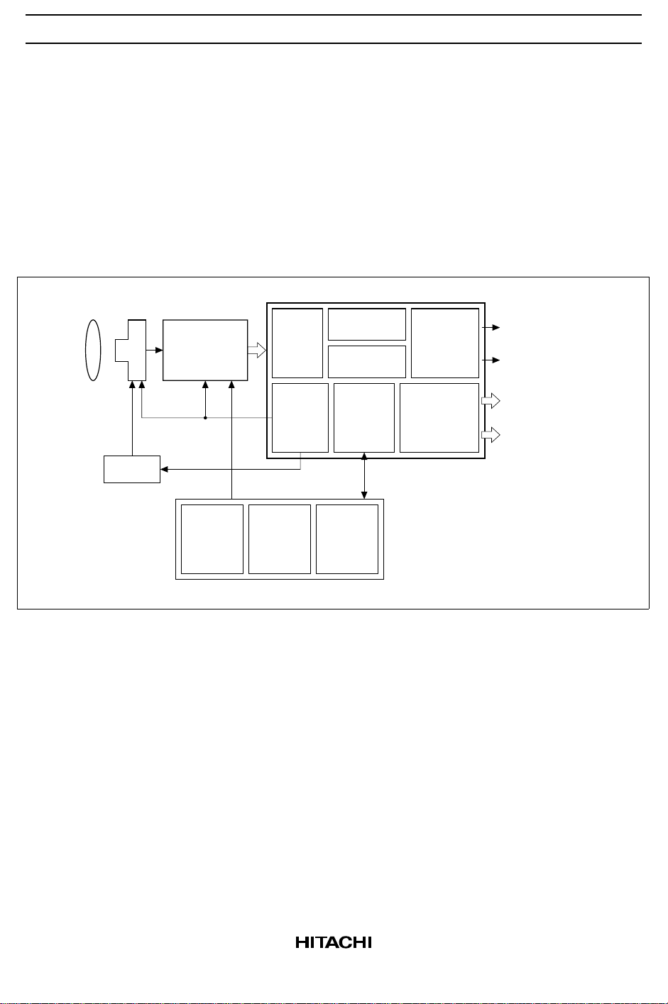
System Block Diagram
HD49815TF
CCD HD49323AF-01Lens
CDS/AGC+
10-bit ADC
Input
line
memory
Color
processing
Luminance
processing
Zoom
processing
C-signal output
Y-signal output
V.Driver
TG
SSG
System
control
8-bit single-chip microcomputer (H8 series)
AE
(iris)
control
Micro-
processor
I/F
AWB
(white
balance)
control
Encode
DAC
R-Y/B-Y
digital output
Y-signal
digital output
2
Page 3
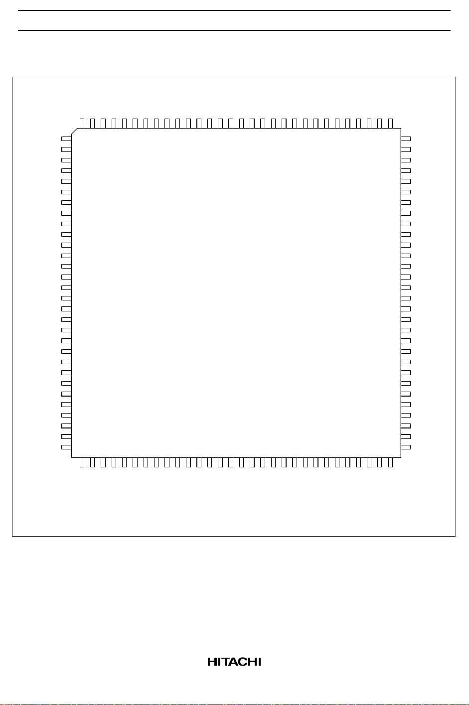
Pin Arrangement
XSG2
XSG1
XV4
XV3
XV2
XV1
DD
RG
VDDH2H1VDDOBP
V
SP2
SP1
VSSVDDDSP_MCK
CPREF
ADCK
AD(1)
AD(2)
AD(3)
AD(4)
AD(5)
HD49815TF
AD(6)
AD(7)
AD(8)
AD(9)
AD(10)
XSUB
DKF_LD
T_CP(TEST)
TY_K
SDI
SDCK
SLD
SDO
EP(1)
EP(2)
BF
HD_IN
M_CK
V
V
FV
HD
CBLK
CSYNC
SCBLK
HSYNC
IDP
V
V
X1I
X1O
IDS
MCK_S
RESET
120 119 118 117 116 115 114 113 112 111 110 109 108 107 106 105 104 103 102 101 100
1
2
3
4
5
6
7
8
9
10
11
12
13
14
DD
15
SS
16
TFP-120
17
18
19
20
21
ID
22
23
24
DD
25
SS
26
27
28
29
30
31
32 33 34 35 36 37 38 39 40 41 42 43 44 45 46 47 48 49 50 51 52 53 54 55 56 57 58 59 60
99 98 97 96 95 94 93 92 91
90
89
88
87
86
85
84
83
82
81
80
79
78
77
76
75
74
73
72
71
70
69
68
67
66
65
64
63
62
61
ZOOM_HD
FP
NME
CPI(1)
CPI(2)
CPI(3)
CPI(4)
CPI(5)
CPI(6)
CPI(7)
CPI(8)
CPO(1)
CPO(2)
CPO(3)
CPO(4)
V
SS
V
DD
CPO(5)
CPO(6)
CPO(7)
CPO(8)
YPI(1)
YPI(2)
YPI(3)
YPI(4)
YPI(5)
YPI(6)
YPI(7)
YPI(8)
YPO(1)
PLL_P
PLL_N
VR
X2I
X2O
FSC
SS
SS
DD
V
AV
SS
DD
V
AV
V
CBU
C_OUT
CBL
REXT
Y_OUT
SS
SS
DD
V
AV
SS
DD
V
V
V
DICK
YPO(8)
YPO(7)
YPO(6)
YPO(5)
YPO(4)
YPO(3)
NRYBY
YPO(2)
(Top view)
3
Page 4

HD49815TF
Pin Description
I/O
Pin No. Symbol Pin Name I/O Description
1 XSUB CCD shutter pulse O CCD control pulse ZC2R
2 DKF_LD Line input LD I Line input dedicated load ICS
3 T_CP Test I Test pin (GND input) IC
4 TY_K Title SW I Title-killer SW (1 = On, 0 = Off) ICD
5 SDI State data input I State data-setting data input IC
6 SDCK State data clock I State data-setting clock ICS
7 SLD State data load pulse I State data-latch pulse ICS
8 SDO AWB, AE, data output O AWB, AE, and AF detection-data output ZC2R
9 EP (1) AE window pulse 1 O Iris detection-area-setting pulse:
SP-A7 [8] output changeover
10 EP (2) AE window pulse 2 O Iris detection-area-setting pulse:
SP-A7 [8] output changeover
11 BF Burst flag O Burst flag output ICZC2R
12 HD_IN External CSYNC input I External CSYNC input ICSD
13 M_CK Microprocessor clock O Microprocessor clock output
(1/2 or 1/4 dividing of X’tal 1)
14 V
15 V
DD
SS
VCC2 — 3.3 V power supply VCCI
GND — GND GNDI
16 FV Field vertical output O Vertical synchronization pulse ICZC2R
17 HD HD output O Horizontal synchronization pulse ICZC2R
18 CBLK Blanking pulse O Blanking pulse ICZC2R
19 CSYNC SYNC output O SYNC pulse ICZC2R
20 SCBLK SC blanking pulse O Subcarrier blanking pulse (SECAM) ICZC2R
21 HSYNC Horizontal SYNC O Horizontal SYNC pulse (SECAM) OC2R
22 ID Identity O SECAM determination pulse OC2R
23 IDP Identity pulse O SECAM determination pulse ICZC2R
24 V
25 V
DD
SS
VCC2 — 3.3 V power supply VCCC
GND — GND GNDC
26 X1I X’tal 1 input I 2fsc oscillator input IQ3
27 X1O X’tal 1 output O 2fsc oscillator output OQ3
28 IDS Line ID reset input I Line-determination-signal input ICD
29 MCK_S MCK output SW I Pin 13 MCK dividing setting SW
(1 = 1/2, 0 = 1/4)
30 RESET Reset I Reset: to restore the initial data settings ICS
Format
ICZC2R
ICZC2R
OC2R
IC
4
Page 5

HD49815TF
Pin Description (cont)
I/O
Pin No. Symbol Pin Name I/O Description
31 PLL_N PLL negative O PLL signal output ZC2
32 PLL_P PLL positive O PLL signal output ZC2
33 VR Vertical reset I Vertical synchronization signal input ICSD
34 X2I X’tal 2 input I 4fsc oscillator input IQ2
35 X2O X’tal 2 output O 4fsc oscillator output OQ2
36 FSC Sub carrier frequency O fsc output ICZC2R
37 V
38 AV
39 V
40 AV
41 V
SS
DD
SS
DD
SS
GND — GND GNDA
Analog VCC2 — Analog system power supply: 3.3 V VCCA
GND — GND GNDA
Analog VCC2 — Analog system power supply: 3.3 V VCCA
GND — GND GNDA
42 C_OUT C analog signal output O Chrominance-signal analog output OA
43 CBU Current buffer upper I D/A upper current source IA
44 CBL Current buffer lower I D/A lower current source IA
45 REXT Reference resister EXT I Reference voltage input IA
46 Y_OUT Y analog signal output O Luminance-signal analog output OA
47 V
48 AV
49 V
50 V
51 V
SS
DD
SS
DD
SS
GND — GND GNDA
Analog VCC2 — Analog system power supply: 3.3 V VCCA
GND — GND GNDA
VCC2 — Digital system power supply: 3.3 V VCCI
GND — GND GNDI
52 DICK Digital interface clock O Digital interface clock output ICZC2R
53 NRYBY R-Y, B-Y phase output O Color-difference signal phase clock ICZC2R
54 YPO (8) Y parallel output (8); MSB O Luminance-signal digital output MSB OC2R
55 YPO (7) Y parallel output (7) O Luminance-signal digital output OC2R
56 YPO (6) Y parallel output (6) O Luminance-signal digital output OC2R
57 YPO (5) Y parallel output (5) O Luminance-signal digital output OC2R
58 YPO (4) Y parallel output (4) O Luminance-signal digital output OC2R
59 YPO (3) Y parallel output (3) O Luminance-signal digital output OC2R
60 YPO (2) Y parallel output (2) O Luminance-signal digital output OC2R
61 YPO (1) Y parallel output (1) ; LSB O Luminance-signal digital output LSB OC2R
62 YPI (8) Y parallel input (8); MSB I Luminance-signal digital input MSB ICD
63 YPI (7) Y parallel input (7) I Luminance-signal digital input ICD
64 YPI (6) Y parallel input (6) I Luminance-signal digital input ICD
Format
5
Page 6

HD49815TF
Pin Description (cont)
I/O
Pin No. Symbol Pin Name I/O Description
65 YPI (5) Y parallel input (5) I Luminance-signal digital input ICD
66 YPI (4) Y parallel input (4) I Luminance-signal digital input ICD
67 YPI (3) Y parallel input (3) I Luminance-signal digital input ICD
68 YPI (2) Y parallel input (2) I Luminance-signal digital input ICD
69 YPI (1) Y parallel input (1); LSB I Luminance-signal digital input LSB ICD
70 CPO (8) C parallel output (8); MSB O Chrominance-signal digital output
MSB
71 CPO (7) C parallel output (7) O Chrominance-signal digital output OC2R
72 CPO (6) C parallel output (6) O Chrominance-signal digital output OC2R
73 CPO (5) C parallel output (5) O Chrominance-signal digital output OC2R
74 V
75 V
76 CPO (4) C parallel output (4) O Chrominance-signal digital output OC2R
77 CPO (3) C parallel output (3) O Chrominance-signal digital output OC2R
78 CPO (2) C parallel output (2) O Chrominance-signal digital output OC2R
79 CPO (1) C parallel output (1); LSB O Chrominance-signal digital output
80 CPI (8) C parallel input (8); MSB I Chrominance-signal digital input
81 CPI (7) C parallel input (7) I Chrominance-signal digital input ICD
82 CPI (6) C parallel input (6) I Chrominance-signal digital input ICD
83 CPI (5) C parallel input (5) I Chrominance-signal digital input ICD
84 CPI (4) C parallel input (4) I Chrominance-signal digital input ICD
85 CPI (3) C parallel input (3) I Chrominance-signal digital input ICD
86 CPI (2) C parallel input (2) I Chrominance-signal digital input ICD
87 CPI (1) C parallel input (1); LSB I Chrominance-signal digital input
88 NME Memory HD output O Line memory control output ICZC2DR
89 FP Field pulse O Field pulse ICZC2R
90 ZOOM_HD Zoom HD output O Horizontal synchronization signal ICZC2R
91 AD (10) AD input (10); MSB I A/D data input MSB IC
92 AD (9) AD input (9) I A/D data input IC
93 AD (8) AD input (8) I A/D data input IC
94 AD (7) AD input (7) I A/D data input IC
DD
SS
VCC2 — 3.3 V power supply VCCO
GND — GND GNDO
LSB
MSB
LSB
Format
OC2R
OC2R
ICD
ICD
6
Page 7

HD49815TF
Pin Description (cont)
I/O
Pin No. Symbol Pin Name I/O Description
95 AD (6) AD input (6) I A/D data input IC
96 AD (5) AD input (5) I A/D data input IC
97 AD (4) AD input (4) I A/D data input IC
98 AD (3) AD input (3) I A/D data input IC
99 AD (2) AD input (2) I A/D data input IC
100 AD (1) AD input (1); LSB I A/D data input LSB IC
101 ADCK AD clock O A/D converter clock ICZC2R
102 CPREF Clamp reference output O Clamp reference pulse 2C3
103 DSP_MCK Microprocessor clock
output
104 V
105 V
DD
SS
VCC2 — 3.3 V power supply VCCO
GND — GND GNDO
O Microprocessor clock output:
SP-A7 [8] output changeover
106 SP1 Sampling pulse 1 O Sampling pulse for the AGC/CDSICICZC2
Format
ICZC2R
107 SP2 Sampling pulse 2 O Sampling pulse for the AGC/CDSICICZC2
108 OBP OBP pulse O Optical black-pulse output ICZC2R
109 V
DD
VCC1 — 3 V or 5 V power supply
VCCC35
(H1/H2 power supply)
110 H1 H1 O CCD-sensor horizontal drive pulse OC3R
111 H2 H2 O CCD-sensor horizontal drive pulse OC3R
112 V
DD
VCC1 — 5 V power supply
VCCC5
(RG power supply)
113 RG Reset gate O CCD-sensor control reset gate ZC3R
114 V
DD
VCC2 — 3.3 V power supply VCCO
115 XV1 XV1 O CCD-sensor vertical control pulse ICZC2R
116 XV2 XV2 O CCD-sensor vertical control pulse ICZC2R
117 XV3 XV3 O CCD-sensor vertical control pulse ICZC2R
118 XV4 XV4 O CCD-sensor vertical control pulse ICZC2R
119 XSG1 XSG1 O CCD-sensor vertical control pulse ZC2R
120 XSG2 XSG2 O CCD-sensor vertical control pulse ZC2R
7
Page 8

HD49815TF
Description of I/O Format
I/O Format Contents
IC CMOS level input
ICD CMOS level input with pull-down resistor
ICS CMOS level schmitt input
ICSD CMOS level input with pull-down resistor
ICZC2 CMOS level common I/O (4 mA)
ICZC2DR CMOS level common I/O with pull-down resistor and through-put control (4 mA)
ICZC2R CMOS level common I/O with through-put control (4 mA)
OC2R CMOS level output with through-put control (4 mA)
OC3R CMOS level output with through-put control (8 mA)
IQ2 Crystal oscillator input
OQ2 Crystal oscillator output
IQ3 Crystal oscillator input
OQ3 Crystal oscillator output
ZC2 CMOS-level three-state output (4 mA)
ZC2R CMOS-level three-state output with through-put control (4 mA)
ZC3 CMOS-level three-state output (8 mA)
ZC3R CMOS-level three-state output with through-put control (8 mA)
VCCI Core system power supply: 3 V
VCCO Puddling system power supply: 3 V
VCCC Common power supply: 3 V
VCCC5 Common power supply: 5 V for pin 112
VCCC35 Common power supply: 3 or 5 V for pin 109
GNDI Core system GND
GNDO Puddling system GND
GNDC Common GND
IA Analog input
OA Analog output
VCCA Analog power supply
GNDA Analog GND
Notes: 1. Pin 113 is used for 5 V system output.
2. Pins 110 and 111 are used for 3 V or 5 V system output. They depend on the voltage of pin 109.
8
Page 9

Block Diagram
16
HD49815TF
16
AE
detection
AF
detection
Base
clipp-
Axis
conver-
C-G
correc-
Gamma
Gain
RGB
+
RGB
Matrix
Pre-
Filter
C-
limit
SW
LINE
+
ing
sion
tion
+
sion
Axis
(WB)
conver-
YL
Matrix
WB
RGB Setup
WB
tion
detec-
+
Fade
Highlight
enhancer
tion
correc-
Gamma
+
correction
Luminance
H.V
enhancer
7.5IRE
Y Setup
SW SW
SW
SW
Y out
Y.DAC
8-bit
CLK
conver-
+
C
Zoom
function
sion
BLK
Titler MOD
C.DAC
Y
SW
SW
C out
8-bit
SDO
SLD
16
SDCK
SDI
16 16 16
Microprocessor interface
CPI
YPI
CPO
16 1616
YPO
16
Digital interface
LPF LPF
SW
10-bit
A/D input
DL
1HDL
AGC
De-Knee
16
1HDL
control
Memory
16
16
X’tal 1
Timing
generator
16
X’tal 2
16
SSG
16
M_CK
H1, H2, RG, XV1 to 4
XSG1,2, XSUB
16DSP_MCK
16
to
Vdriver
CCD
FV, HD, MCK, MCKS
PLLP, PLLN, fsc, CBLK
CP, CSYNC, EP1-3
ADCK, OBP, SP1
SP2, PBLK
16
to
CDS/AGC
IDP, SCBLK, etc.
16
FV,
CHD etc.
9
Page 10

HD49815TF
Absolute Maximum Ratings (Ta = 25°C)
Item Symbol Ratings Unit
Power supply voltage V
Pin voltage (5 V operation block) Vt5V –0.2 to VCC1 +0.2 V
Pin voltage (3 V operation block) Vt3V –0.2 to VCC2 +0.2 V
Output current Per output Io –32 to +32 mA
Per GND-VCC pair Iot –72 to +72 mA
Allowable power dissipation Popr 450 mW
Operating temperature Topr –10 to +75 °C
Storage temperature With bias Tbias –10 to +75 °C
Without bias Tstg –40 to +125 °C
Notes: 1. Using this LSI at values in excess of the absolute maximum ratings may permanently damage
the LSI. The LSI should normally be operated under the conditions specified for the electrical
characteristics. Exceeding these conditions may lead to incorrect operation and may adversely
affect LSI reliability.
2. All voltage values are referenced to GND = 0 V.
3. The pin voltage ratings also apply to the NC pins.
4. V
1 indicates the 5 V system power supply and VCC2 indicates the 3 V system power supply.
CC
CC
–0.2 to +6.8 V
10
Page 11

HD49815TF
O
O
O
O
CC
Electrical Characteristics (VCC1 = 4.75 V to 5.25 V, VCC2 = 2.85 V to 3.15 V,
AVCC = 2.85 V to 3.15 V, Ta = 25°C)
Test Conditions
Item Symbol Min Typ Max Unit
CMOS-level V
input voltage V
IHC
ILC
CMOS schmitt VTC+ 2.50 — VCC2VV
input voltage VTC– 0.0 — 0.60 V VCC2 = 3 V
Output voltage V
Input leakage current I
Output leakage current I
Pull-down current I
OHC1
V
OLC1
V
OHC2
V
OLC2
LI
LO
PD
Power dissipation Popr — — 450 mW VCC1 = 5 V,
Analog output voltage
Vfull 0.80 1.00 1.20 V 3, 4
(full scale)
Analog output voltage
Vzero –0.20 0.00 0.20 V
(zero scale)
Differential linearity DNL –2.0 — 2.0 LSB
Notes: 1. Output voltage must be measured in the steady state.
2. Except for pins that include a pull-down resistor.
3. Guaranteed at CBU = 0.1 µF, CBL = 0.1 µF, REXT = 3.4 kΩ, analog output load resistance = 500
Ω, and Ta = 25°C.
4. Applied to pins indicated as OA in the I/O format column of the pin-functions table.
5. Because V
6. Because V
7. V
1, VCC2, and AVCC indicate the 5 V system power supply, the 3 V system power supply, and
CC
of pin 31 cannot be measured logically, it was not tested.
OH
of pin 32 cannot be measured logically, it was not tested.
OL
the analog system power supply, respectively. V
8. The voltage range of pin 109 (VCCC35) is V
VCC2×0.75 — VCC2V
0.0 — VCC2×0.20 V
1 = 5 V
CC
VCC1–0.5 — — V I
= –200 µA
H
5 V system pin
— — 0.4 V I
= 200 µA
L
5 V system pin
VCC2–0.5 — — V I
= –200 µA
H
3 V system pin
— — 0.4 V I
= 200 µA
L
3 V system pin
— — 1.0 µAVIN = 0 V to V
— — 1.0 µA Output Hi-Z
conditions
5 — 100 µAVIN = VCC2 = 3 V
V
2 = 3 V,
AV
= 3 V
CC
indicates VCC1, VCC2, and AVCC.
CC
= 2.85 V to 5.25 V.
CC
Note
1
1, 5
1, 6
2
CC
2
3
11
Page 12

HD49815TF
Crystal Oscillation Circuit
1. Measuring conditions
The oscillation frequency was measured under the following conditions.
VCC1 = 5.0 V
VCC2 = 3 V
Ta = 25°C
8 MHz, 20 MHz, and 24 MHz:
Rf = 1 to 10 MΩ
Cin, Cout = 20 pF (±20 pF)
32 MHz:
Rf = 1 to 10 MΩ
Cin = 20 pF (±20 pF)
Cout = 100 pF (±20 pF), Co = 15 pF (±5 pF), Lout = 1 µH
The conditions above may be changed within the range of measuring conditions.
2. Measuring method
Under the measuring conditions above, two methods were tested.
fmin. = 20 MHz, and fmax. = 32 MHz (applied to pins 26 and 27)
fmin. = 8 MHz, and fmax. = 24 MHz (applied to pins 34 and 35)
Note: The oscillation start time tosc is max. = 200 ms.
3. Measuring circuit
To the internal circuit
Xin
Note: The part enclosed by the dotted line in the above
circuit is used when measuring at 32 MHz.
Xout
Dividing
counter
CoutCin
Co Lout
Monitor pin
Counter
Figure 1 Measuring Circuit
12
Page 13

Built-in Functions and System Configuration
System Configuration
HD49815TF
CCD HD49323AF-01Lens
CDS/AGC+
10-bit ADC
Input
line
memory
processing
Luminance
processing
Color
Zoom
processing
HD49815TF
C-signal output
Y-signal output
R-Y/B-Y
digital output
Y-signal
digital output
V.Driver
SP1/2
H1, H2
XV1 to 4
AGC gain setting
System
control
8-bit single-chip microcomputer (H8 series)
TG
SSG
AE
(iris)
control
Micro-
processor
I/F
Initial setting resistor input and
AE, AWB detection data output
AWB
(white
balance)
control
Encode
DAC
Figure 2 System Configuration
System Description
1. CCD
The following lists the pixels of the CCD sensors that can be used with the HD49815TF. For other
pixel numbers, contact our sales dept.
512 (H) × 492 (V) NTSC
512 (H) × 582 (V) PAL
682 (H) × 492 (V) NTSC
681 (H) × 582 (V) PAL
2. CDS/AGC + 10-bit ADC
The HD49323AF-01 (manufactured by Hitachi) is recommended as an optimal CDS/AGC + 10-bit
ADC IC for the HD49815TF. Since the HD49323AF-01 provides a correlated double sampling circuit
that realizes high S/N and an automatic gain control (AGC) circuit that implements programmable
control of 0 dB to 34.7 dB, it enables a high-image-quality camera system when used in conjunction
with the HD49815TF.
13
Page 14

HD49815TF
3. 8-bit single-chip microcomputer
The 8-bit single-chip microcomputer controls the system. It receives the image detection data that the
HD49815TF is gathering and implements automatic iris control (AE), automatic white balance control
(AWB), and automatic focus control (AF).
When setting the power on, this microcomputer implements the initial setting to the state data of the
HD49815TF.
For details on the state data, see “Hitachi Camera DSP (HD49815TF) State Data”.
Built-in Functions
1. Input line memory block
A/D input
10-bit
16
16
De-Knee
AGC
Memory
control
1HDL
1HDL
DL
+
To the color-signal
processing block
To the luminance-signal
processing block
Figure 3 Input Line Memory Block
a. De-knee function
When the CDS/AGC IC at the pre-stage or the external circuit uses the knee circuit to expand the
dynamic range of the signal, the de-knee (inverse knee) circuit returns the signal converted by the
knee circuit to the original state.
The de-knee point can be set in State Data SP_A0 [1]. The gain of the high-luminance block is 1/2.
b. AGC function
A digital AGC circuit is provided. The AGC gain can be set in State Data SP_A0 [2] from 1 to 16
times.
c. 1H delay line (1HDL) function
This circuit obtains horizontal efficient pixels of the CCD output signal. The number of efficient
pixels is set in State Data SP_A0 [9, 10] and TM_A0 [14] MCSET.
14
Page 15

2. Color-signal processing block
HD49815TF
From
the input
line
memory
block
LINESWC-
limit
Pre-
Filter
RGB
Matrix
RGB Setup
+
RGB
Gain
+
WB
To the luminance
signal processing block
Gamma
correc-
tion
YL
Matrix
C-G
detection block
Axis
conver-
sion
Axis
conver-
sion
(WB)
To the AWB
Base
clipp-
ing
Figure 4 Color-Signal Processing Block
a. C-limit (complementary color clipping level) function
High clipping processing is performed on the complementary color signals independently. High
clipping is set in State Data SP_A2 [0 to 3].
The complementary color signal indicates Gb: (G + Cy), Wr: (Ye + Mg), Wb: (Mg + Cy), and Gr:
(G + Ye).
b. RGB-matrix block
The three primary colors (red, green, and blue) are acquired in the RGB matrix by multiplying
arbitrary coefficients by the four complementary colors (Gb, Wr, Wb, and Gr) and taking the total of
those results. The RGB matrix is designed to support the minimum color moire and to enable free
color reproduction. Arbitrary coefficients are set in State Data SP_A2 [4 to 15]. The following
shows the formula.
KRd
KRa
R
=
KBa
B
KGa
G
KRc
KRb
KBd
KBc
KBb
KGd
KGc
KGb
State Data SP_A2 [4 to 15]
Gb
Wr
Wb
Gr
To
the zoom
function
c. RGB-setup block
The black level of the color signals is variable according to the coefficients of the RGB matrix. The
value calculated by the formula below is subtracted from the color signal to correct the black level.
The subtracted value can be set externally and is set in State Data SP_A3 [0 to 2].
Formula = −[48 × Σ (Matrix data) × 23]
d. RGB-gain block
The RGB gain value acquired in the AWB control is set in the RGB gain circuit to improve the
white reproduction performance. As it is set prior to the gamma correction, it changes the gamma
correction amount. The RGB gain can be set in State Data SP_A3 [3 to 5] from 1 to 256 times.
(The G gain is set from 1 to 128 times.)
15
Page 16

HD49815TF
e. C gamma (γ) correction block
The C gamma correction circuit performs gamma processing on the RGB signal. It is set in State
Data SP_A3 [6 to 9]. Four kinds of values can be set independently, according to the input-signal
level, to acquire optimal gamma characteristics: the C gamma dark (to reduce the gain of the small
signals for improving S/N), C gamma coefficient (to control the expansion of the gamma curve), C
gamma knee (to decide the slope of the large signals), and C gamma limit (to perform high-clipping
processing for the input signal of the C gamma circuit).
f. YL matrix block
The luminance level changes according to the color temperature of the imaged object. Set State
Data SP_A5 [12, 13] for the luminance correction. To correct the luminance, create YL from the
three primary colors (R, G, and B) and convert it to the luminance signal level. The YL matrix
circuit creates the YL level from the RGB signal.
The YL matrix is set in State Data SP_A3 [11 to 13].
g. The axis-conversion (C-Y matrix) block
The C-Y (color-difference) matrix takes R-G and B-G as its input signals, and creates the R-Y and
B-Y color-difference signals by setting coefficients for those inputs.
The axis-conversion (C-Y matrix) circuits are set in State Data SP_A8 [0 to 5].
h. Base-clipping block
Since base clipping is performed on the color-difference signals, the base-clipping circuit has the
characteristics of clipping the sections near axes on a vector scope.
This circuit is set in State Data SP_A8 [8].
3. Luminance-signal-processing block
To
the AWBdetection block
+
7.5IRE
From
the input
line
memory
block
H.V
enhancer
Luminance
correction
from
YL matrix
+
Y Setup
Gamma
correc-
tion
Highlight
enhancer
Fade
Figure 5 Luminance-Signal-Processing Block
a. H-enhancer function
The H-enhancer circuit allows the core level, the enhancer gain, and the noise coefficient to be set
independently to acquire optimal characteristics.
This circuit is set in State Data SP_A4 [4 to 7].
b. V-enhancer function
The V-enhancer circuit allows the enhancer coefficient to be set and can control the gain for only
those signal components that exceed the set core level.
This circuit is set in State Data SP_A4 [8 to 10].
To
the zoom
function
16
Page 17

HD49815TF
c. Luminance correction
The ratio of the red and blue levels changes according to the color temperature of the imaged object.
For example, if a red object is imaged at a low color temperature, the luminance level increases and
the object appears to have a lower chrominance. Therefore, the luminance correction circuit
performs luminance-correction processing to implement color depth reproduction.
The luminance-correction circuit is set in State Data SP_A5 [12, 13].
d. Y setup
Since the OB clamp processes the signal, the black level of the 10-bit signal input to the
HD49815TF is fixed to 48/1024. The Y-setup circuit subtracts 48 at the black level. However,
when 48 at the black level differs due to the noise mixed in the analog signal, the Y-setup circuit
subtracts that value.
The Y-setup circuit is set in State Data SP_A5 [6].
e. Gamma correction
The gamma-correction circuit implements the gamma-correction processing for the separated Y
signal. Four kinds of values can be set independently, according to the input-signal level, to acquire
optimal gamma characteristics: the gamma input limit, the gamma knee coefficient, the gamma
coefficient, and the gamma black clipping.
The gamma correction circuit is set in State Data SP_A5 [1 to 4].
f. Highlight enhancer
For input-Y signal levels in excess of 100 IRE, the highlight enhancer implements highlight
enhancer processing.
This circuit is set in State Data SP_A5 [0, 5, and 14].
g. Fade
The fade circuit amplifies the luminance signal by a factor of 0 to 1.
This circuit is set in State Data SP_A5 [9].
4. Zoom, encode block, TG, SSG, and AWB and AE detection blocks
a. Zoom processing
The Y, R-Y, and B-Y signals completed the color-signal processing and the luminance-signal
processing can be electronically zoomed by a factor of 1 to 256.
After clipping CCD signals for V direction, zoom circuit clips these signals for H direction, and
expand these signals for H and V directions.
The zooming times and the read starting position for the V and H directions are set in State Data
TM_A2 [3, 4, 5, 6, 8, and 9] and ZM_A0 to 6.
b. Encode block
This circuit encodes the signals completed the color-signal processing, the luminance-signal
processing, and the zoom processing as the NTSC/PAL TV-monitor method.
A DAC that converts the digital signal to an analog signal is provided. The DAC has two channels:
one for R-Y signals and one for B-Y signals.
17
Page 18

HD49815TF
c. TG and SSG
The TG generates the signals required to drive the CCD sensor (H1, H2, RG, SG1/2, and the V
transfer pulse), and the CDS/AGC control signals (SP1 and SP2).
In addition, the SSG generates the signals to synchronize with the TV monitor (the Sync signal).
The drive timing of the generated signals differs according to the manufacturer and the
specifications of the CCD sensor. Setting the state data enables setting of any timing.
The state data of TG and SSG can be set in TM_A0, A1, A2, A3, and A8.
d. AWB- and AE-detection blocks
The HD49815TF provides automatic white-balance (AWB) and automatic-iris (AE) detection
circuits that are indispensable for a camera.
The AWB-detection block takes the R-Y and B-Y color-difference signals completed the colorsignal processing, and converts to the R-B and MG-G axes. The converted signals are sent to
circuits for the white detection to obtain white signal components only, and the white-color
difference value is detected. The 8-bit single-chip microcomputer acquires this detection data, and
controls the R and B gains to produce the true white.
The State Data of the AWB detection is AWB_A0 and A8.
The AE-detection block divides the CCD output signal converted to digital by the 10-bit ADC to six
arbitrary areas, and performs integration processing. This function enables detection of the lighting
level of the image signal.
The 8-bit single-chip microcomputer acquires this detection data, and controls the accumulation
amount (the shutter) of the CCD sensor or the iris motor of the lens to maintain the proper lighting.
The State Data of the AF detection is AE_A0 to A7 and A8.
18
Page 19

Microcomputer Interface Specifications
• Write format
SLD
(Pin 7)
SDCK
(Pin 6)
HD49815TF
SDI
(Pin 5)
LSB MSB
D1
D2D3D4D5D6D7D8 D1
1 byte
Data (N byte)
LSB LSBMSB
D2D3D4D5D6D7D8
Address
STAL STAH
D2D3D4D5D6D7D8D1
Function address
(write address)
MSB
STD3-----STH2-----STD1
• Read format
SLD
(Pin 7)
SDCK
(Pin 6)
SDI
(Pin 5)
LSB LSBMSB
D2D3D4D5D6D7D8
D1
D2D3D4D5D6D7D8D1
MSB
1 byte or 2 byte
Function address
LSB
MSB
SDO
STAL STAH
Hi-Z Hi-Z
(Pin 8)
Data
(N byte)
Notes: Synchronous serial transfer (The microcomputer serial port can be used.)
1.
Transfer frequency: 3.58 MHz or lower
2.
Data and address are handled in a byte unit.
3.
The clock and load pulse are used in common for read/write.
4.
19
Page 20

HD49815TF
Data Transfer Specification
For data transfer between the HD49815TF and the microcomputer, two types (N and E for write, and R1
and R2 for read) are available. The following table shows the relationship between the function block and
the transfer specifications. On the next page, the details of the transfer specifications are described.
Transfer
Function Block Transfer Mode
Signal processing W N SP_A0, 2 to 5, 7 to 10, 15
TM W N TM_A3, 15
R R1 TMR_A0
Iris W N AE_A0 to 7
R R2 AE_A8
White balance W N AWB_A0
R R1 AWB_A8
AF W N AF_A0 to 3
R R1 AF_A8 to 13
ZOOM W N ZM_A0 to 6
Note: 1. Transfer specifications
Type N : Normal transfer from the microcomputer to the DSP
Type E : Transfer using the set pulse (synchronous with VD) or the reset signal (used as a
synchronous pulse in the DSP) sent from the microcomputer to the RS latch in the
DSP
Note: This cannot be set during the standby mode.
Type R1 : Data transfer (1) from the DSP to microcomputer
Type R2 : Data transfer (2) from the DSP to microcomputer
Specifications *
E TM_A0 to 2, 8, 10 to 12
1
Related Address
20
Page 21

• Type N
Transfer
specification
N
• Type E
Transfer
specification
E
SLD
(Pin 7)
SDCK
(Pin 6)
SLD
(Pin 7)
SDCK
(Pin 6)
Pulse Timing Conditions
A = 100 ns or more
B = 100 ns or more
C = 100 ns or more
ABC
Pulse Timing Conditions
0.5 / fs + 100 ns or more
A
2 / fs + 100 ns or more
B
5.5 / fs + 100 ns or more
A
B
D
D
fs
Sensor clock
HD49815TF
270,000
pixels
150 ns
or more
300 ns
or more
650 ns
or more
100 ns
410,000
pixels
135 ns
or more
240 ns
or more
485 ns
or more
70 ns
• Type R1
Transfer
specification
R1
• Type R2
Transfer
specification
R2
SLD
(Pin 7)
SDCK
(Pin 6)
SLD
(Pin 7)
SDCK
(Pin 6)
Pulse Timing Conditions
A = 100 ns or more
B = 100 ns or more
D = 400 ns or more
Do not read the white balance data and the
AB
D
Pulse Timing Conditions
AB
D
AF read data within the 1H period from the
start of the V blanking.
A = 100 ns or more
B = 100 ns or more
D {1 / fs × (32 + 5)
+ 400 ns} or more
fs
Sensor clock
270,000
pixels
4.1 µs
or more
100 ns
410,000
pixels
2.99
µs
or more
70 ns
21
Page 22

HD49815TF
Note: 2 to 9. Function addresses
The following table shows the function addresses for each function block (during state data
transfer) and the data to be transferred from the microcomputer.
Table 2 Function Addresses for each Function Block and State Data
List of Data Transferred Remarks
2
Signal
processing
(Setting
example)
3
TM write
(Setting
example)
4
TM read
AE
AWB
AF
ZOOM
Function Address STAH STAL STD1 STD2
D8 D7 D6 D5 D4 D3 D2 D1 D8 D7 D6 D5 D4 D3 D2 D1 D8 D7 D6 D5 D4 D3 D2 D1 D8 D7 D6 D5 D4 D3 D2 D1
00000000∗∗∗∗∗∗∗∗∗∗∗∗∗∗∗∗∗∗∗∗∗∗∗∗
0000000000001001
Function Address
D8 D7 D6 D5 D4 D3 D2 D1 D8 D7 D6 D5 D4 D3 D2 D1 D8 D7 D6 D5 D4 D3 D2 D1 D8 D7 D6 D5 D4 D3 D2 D1
00000001∗∗∗∗∗∗∗∗∗∗∗∗∗∗∗∗∗∗∗∗∗∗∗∗
0000000100001110
Function Address
D8 D7 D6 D5
00001001
Function Address
D8 D7 D6 D5 D4 D3 D2 D1 D8 D7 D6 D5 D4 D3 D2 D1 D8 D7 D6 D5 D4 D3 D2 D1 D8 D7 D6 D5 D4 D3 D2 D1
00010∗∗∗∗∗∗∗∗∗∗∗ ∗∗∗∗00000000
00010100
5
W
Function Address
D8
D7 D6 D5 D4 D3 D2 D1 D8 D7 D6 D5 D4 D3 D2 D1 D8 D7 D6 D5 D4 D3 D2 D1 D8 D7 D6 D5 D4 D3 D2 D1
00000001∗∗∗∗∗∗∗∗∗∗∗∗∗00000000
0000000110100010
Function Address STAH STAL
6
D8 D7 D6 D5 D4 D3 D2 D1 D8 D7 D6 D5 D4 D3 D2 D1
R
00011000 ∗∗∗∗
Function Address
D8 D7 D6 D5 D4 D3 D2 D1 D8 D7 D6 D5 D4 D3 D2 D1 D8 D7 D6 D5 D4 D3 D2 D1 D8 D7 D6 D5 D4 D3 D2 D1
00100 ∗∗∗∗∗∗∗∗∗∗∗∗∗00000000
00100 00001
7
W
Function Address
D8
D7 D6 D5 D4 D3 D2 D1 D8 D7 D6 D5 D4 D3 D2 D1 D8 D7 D6 D5 D4 D3 D2 D1
0000000∗∗∗∗∗∗∗∗∗∗∗∗∗∗
0000000110110011
Function Address
8
D8 D7 D6 D5 D4 D3 D2 D1
R
00101000
Function Address
D8 D7 D6 D5 D4 D3 D2 D1 D8 D7 D6 D5 D4 D3 D2 D1
00110∗∗∗∗∗∗∗∗∗∗∗
00110000
9
Function Address
W
D8
D7 D6 D5 D4 D3 D2 D1 D8 D7 D6 D5 D4 D3 D2 D1 D8 D7 D6 D5 D4 D3 D2 D1
0000000111000∗∗∗∗∗∗∗∗∗∗∗
0000000111000101
Function Address
10
D8 D7 D6 D5 D4 D3 D2 D1
R
00111∗∗∗
D8 D7 D6 D5 D4 D3 D2 D1
10110∗∗∗
W
D4 D3 D2 D1
Header
STAH STAL STD1 STD2
Data read for automatic phase adjustment for SP1, SP2, and RG
STAHADATA STAL STD1 STD2
D3 D2D1
STAH STALADATA STD1 STD2
STAHADATA STAL STD1 STD2
STAH STALADATA STD1
STAHADATA STAL
D4 D3D2 D1
STAH STALADATA STD1
Data 1
D8 D7D6 D5 D4D3 D2 D1
D8 D7D6 D5 D4D3 D2 D1
00000000
D5 D4D3 D2 D1
Read area setting by STAL (4 bits)
D6 D5D4 D3 D2D1
D8 D7D6 D5 D4D3 D2 D1
White balance read
HPF bandwidth selection
Base-clip quantity setting, etc.
D8 D7D6 D5 D4D3 D2 D1
Vf fetch address (read_cycle)
Data 2
00000000
00000000
Window setting
for white balance
WB detection
axis phase setting
Setting for integration
and display gate
Data 3
Data 6Data 5Data 4
D9
This example
is related to
SP-A0[9].
This example
is related to
TM-A0 [14].
This example
is related to
the IRIS peak
detection area.
This example
is related to
the window
H count 3.
This example
is related to
the offset R-B.
This example
is related to
the V count 2.
This example
is related to
the HRF
bandwidth
selection.
This example
is related to
the differential
gate of V-end.
Note: For the ZOOM, the transfer of in total of seven bytes is required for the header and data 1 to 6.
22
Page 23

Digital Interface Timing
• The output specification and timing of the digital interface output (Y, R-Y, B-Y)
NRYBY
DICK
4 : 2 : 2 output timing
HD49815TF
CPO (1 to 8) R-Y2 R-Y4 B-Y4B-Y1
YPO (1 to 8) Y2 Y4 Y5Y3
• Detailed specifications of digital interface timing
X’tal CLK
DICK output
CPO, YPO
CPI, YPI
NRYBY
R-Y0 B-Y0
Y0 Y1
35 nsec 70 nsec
2 to 15 nsec
20 to 35 nsec
(Reference)
10 to 50 nsec
NRYBY
DICK
CPO, YPO
CPI, YPI
: R-Y/B-Y determination pulse
: Clock dedicated to the digital interface (The clock generated from the external X’tal.)
: Digital interface output terminal
: Digital interface input terminal
23
Page 24

HD49815TF
Package Dimensions
91
16.0 ± 0.2
120
*0.17 ± 0.05
0.15 ± 0.04
16.0 ± 0.2
14
90 61
60
0.4
31
130
M
0.07
1.2
0.10
1.00
1.20 Max
0.15 ± 0.04
*0.17 ± 0.05
Unit: mm
1.0
0° – 8°
0.5 ± 0.1
*Dimension including the plating thickness
Base material dimension
0.10 ± 0.10
Hitachi Code
JEDEC
EIAJ
Weight
(reference value)
TFP-120
—
Conforms
0.5 g
24
Page 25

HD49815TF
Cautions
1. Hitachi neither warrants nor grants licenses of any rights of Hitachi’s or any third party’s patent,
copyright, trademark, or other intellectual property rights for information contained in this document.
Hitachi bears no responsibility for problems that may arise with third party’s rights, including
intellectual property rights, in connection with use of the information contained in this document.
2. Products and product specifications may be subject to change without notice. Confirm that you have
received the latest product standards or specifications before final design, purchase or use.
3. Hitachi makes every attempt to ensure that its products are of high quality and reliability. However,
contact Hitachi’s sales office before using the product in an application that demands especially high
quality and reliability or where its failure or malfunction may directly threaten human life or cause risk
of bodily injury, such as aerospace, aeronautics, nuclear power, combustion control, transportation,
traffic, safety equipment or medical equipment for life support.
4. Design your application so that the product is used within the ranges guaranteed by Hitachi particularly
for maximum rating, operating supply voltage range, heat radiation characteristics, installation
conditions and other characteristics. Hitachi bears no responsibility for failure or damage when used
beyond the guaranteed ranges. Even within the guaranteed ranges, consider normally foreseeable
failure rates or failure modes in semiconductor devices and employ systemic measures such as failsafes, so that the equipment incorporating Hitachi product does not cause bodily injury, fire or other
consequential damage due to operation of the Hitachi product.
5. This product is not designed to be radiation resistant.
6. No one is permitted to reproduce or duplicate, in any form, the whole or part of this document without
written approval from Hitachi.
7. Contact Hitachi’s sales office for any questions regarding this document or Hitachi semiconductor
products.
Hitachi, Ltd.
Semiconductor & Integrated Circuits.
Nippon Bldg., 2-6-2, Ohte-machi, Chiyoda-ku, Tokyo 100-0004, Japan
Tel: Tokyo (03) 3270-2111 Fax: (03) 3270-5109
URL NorthAmerica : http:semiconductor.hitachi.com/
For further information write to:
Hitachi Semiconductor
(America) Inc.
179 East Tasman Drive,
San Jose,CA 95134
Tel: <1> (408) 433-1990
Fax: <1>(408) 433-0223
Europe : http://www.hitachi-eu.com/hel/ecg
Asia (Singapore) : http://www.has.hitachi.com.sg/grp3/sicd/index.htm
Asia (Taiwan) : http://www.hitachi.com.tw/E/Product/SICD_Frame.htm
Asia (HongKong) : http://www.hitachi.com.hk/eng/bo/grp3/index.htm
Japan : http://www.hitachi.co.jp/Sicd/indx.htm
Hitachi Europe GmbH
Electronic components Group
Dornacher Straβe 3
D-85622 Feldkirchen, Munich
Germany
Tel: <49> (89) 9 9180-0
Fax: <49> (89) 9 29 30 00
Hitachi Europe Ltd.
Electronic Components Group.
Whitebrook Park
Lower Cookham Road
Maidenhead
Berkshire SL6 8YA, United Kingdom
Tel: <44> (1628) 585000
Fax: <44> (1628) 778322
Hitachi Asia Pte. Ltd.
16 Collyer Quay #20-00
Hitachi Tower
Singapore 049318
Tel: 535-2100
Fax: 535-1533
Hitachi Asia Ltd.
Taipei Branch Office
3F, Hung Kuo Building. No.167,
Tun-Hwa North Road, Taipei (105)
Tel: <886> (2) 2718-3666
Fax: <886> (2) 2718-8180
Copyright ' Hitachi, Ltd., 1999. All rights reserved. Printed in Japan.
Hitachi Asia (Hong Kong) Ltd.
Group III (Electronic Components)
7/F., North Tower, World Finance Centre,
Harbour City, Canton Road, Tsim Sha Tsui,
Kowloon, Hong Kong
Tel: <852> (2) 735 9218
Fax: <852> (2) 730 0281
Telex: 40815 HITEC HX
25
 Loading...