

Page 1
HD49323AF-01
CDS/AGC & 10-bit A/D Converter
ADE-207-262A (Z)
2nd Edition
Apr. 1999
Description
The HD49323AF-01 is a CMOS IC that provides CCD-AGC analog processing (CDS/AGC) suitable for
CCD camera digital signal processing systems together with a 10-bit A/D converter in a single chip.
Functions
• Correlated Double Sampling
• AGC
• Sample hold
• Offset compensation
• Serial interface control
• 10-bit ADC
• 3 V single operation (2.7 V to 3.6 V)
• Power dissipation: 198 mW (Typ)
• Maximum frequency: 20 MHz (Min)
Features
• Good suppression of CCD output low-frequency noise is achieved through the use of S/H type
correlated double sampling.
• A high S/N ratio is achieved through the use of a AGC type amplifier, and high sensitivity is provided
by a wide cover range.
• An auto offset circuit provides compensation of output DC offset voltage fluctuations due to variations
in AGC amplifier gain.
• AGC, standby mode, offset control, etc., is possible via a serial interface.
• High precision is provided by a 10-bit-resolution A/D converter.
• Version of Hitachi’s previous-generation HD49322BF with improved functions and performance,
including in particular an approximately 3.0 dB improvement in S/N.
Page 2
HD49323AF-01
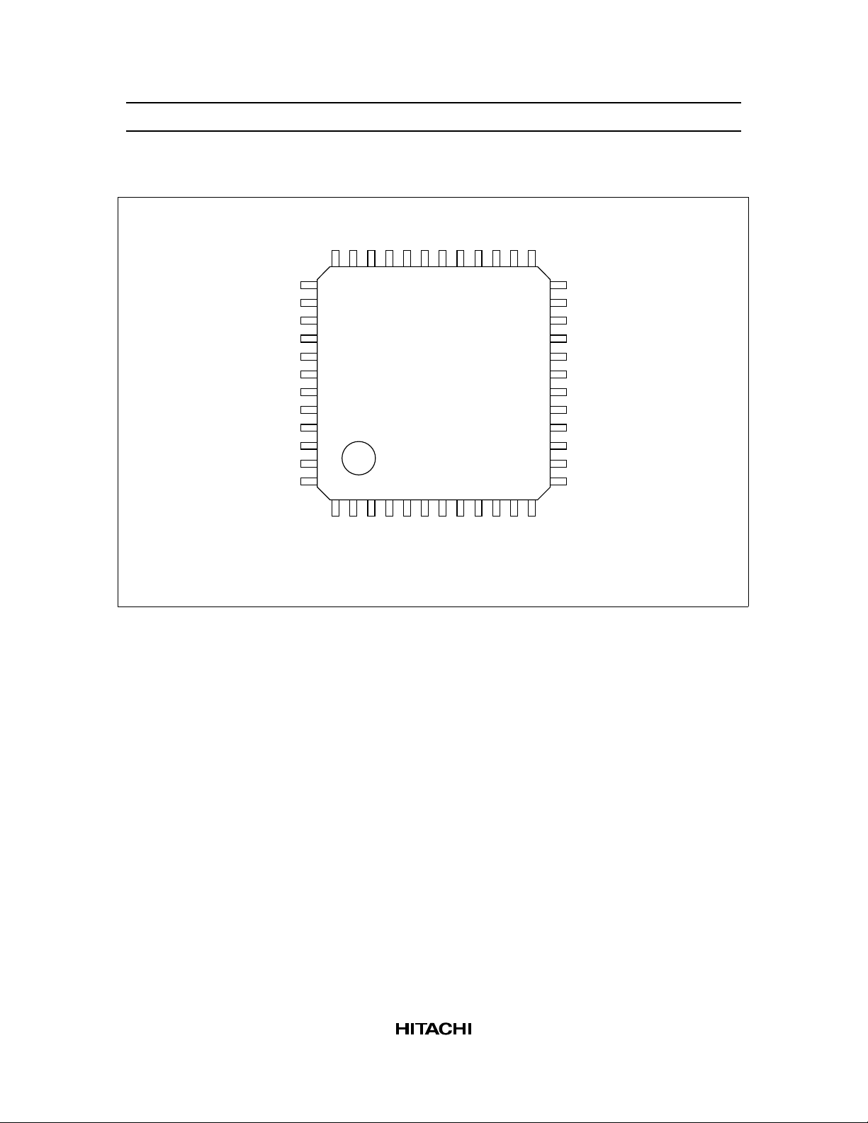
Pin Arrangement
NC
BIAS
VRT
VRM
VRB
AVDDAVSSTESTC
TESTY
CDSIN
AVDDAV
SS
AV
SS
AV
DD
NC
NC
AV
DD
AV
SS
CS
SCK
SDATA
DV
DD
DV
SS
DV
SS
36 35 2734 33 32 31 30 29 28 26 25
37
38
39
40
41
42
43
44
45
46
47
48
12 103456789 1112
D0D1D2D3D4D5D6D7D8
PBLK
(Top view)
D9
24
23
22
21
20
19
18
17
16
15
14
13
NC
VRM2
CLP
NC
AV
DD
AV
SS
SPSIG
SPBLK
OBP
ADCLK
DV
DD
DV
SS
OE
2
Page 3
HD49323AF-01
Pin Description
Analog(A) or
Pin No. Symbol Description I/O
1 PBLK Pre-blanking pin I D
2 D0 Digital output (LSB) O D
3 to 10 D1 to D8 Digital output O D
11 D9 Digital output (MSB) O D
12 NC No connection pin — —
13 OE Digital output enable control pin I D
14 DV
15 DV
SS
DD
Digital ground (0 V) — D
Digital power supply (3 V)
Connect off-chip in common with AV
.
DD
16 ADCLK ADC conversion clock input pin I D
17 OBP Optical black pulse input pin I D
18 SPBLK Black level sampling clock input pin I D
19 SPSIG Signal level sampling clock input pin I D
20 AV
21 AV
SS
DD
Analog ground (0 V) — A
Analog power supply (3 V)
Connect off-chip in common with DV
.
DD
22 NC No connection pin — —
23 CLP Clamp voltage pin
Connect a 0.22 µF or more capacitor between CLP and AV
.
SS
24 VRM2 Reference voltage pin (for CCD offset cancel) — A
25 AV
26 AV
SS
DD
Analog ground (0 V) — A
Analog power supply (3 V)
Connect off-chip in common with DV
.
DD
27 CDSIN CDS input pin I A
28 TESTY Test input pin-Y I A
29 TESTC Test input pin-C I A
30 AV
31 AV
SS
DD
Analog ground (0 V) — A
Analog power supply (3 V)
Connect off-chip in common with DV
.
DD
32 VRB Reference voltage pin 3
Connect a 0.1 µF ceramic capacitor between VRB and AV
.
SS
33 VRM Reference voltage pin 2
Connect a 0.1 µF ceramic capacitor between VRM and AV
.
SS
34 VRT Reference voltage pin 1
Connect a 0.1 µF ceramic capacitor between VRT and AV
.
SS
Digital(D)
—D
—A
—A
—A
—A
—A
—A
—A
3
Page 4
HD49323AF-01
Pin Description (cont)
Analog(A) or
Pin No. Symbol Description I/O
35 BIAS Internal bias pin
Connect a 24 kΩ resistor between BIAS and AVSS.
36 NC No connection pin — —
37 AV
38 AV
SS
DD
Analog ground (0 V) — A
Analog power supply (3 V)
Connect off-chip in common with DV
.
DD
39, 40 NC No connection pin — —
41 AV
42 AV
DD
SS
Analog power supply (3 V)
Connect off-chip in common with DV
.
DD
Analog ground (0 V) — A
43 CS Serial interface control input pin I D
44 SCK Serial clock input pin I D
45 SDATA Serial data input pin I D
46 DV
47, 48 DV
DD
SS
Digital power supply (3 V)
Connect off-chip in common with AV
.
DD
Digital ground (0 V) — D
Digital(D)
—A
—A
—A
—D
4
Page 5
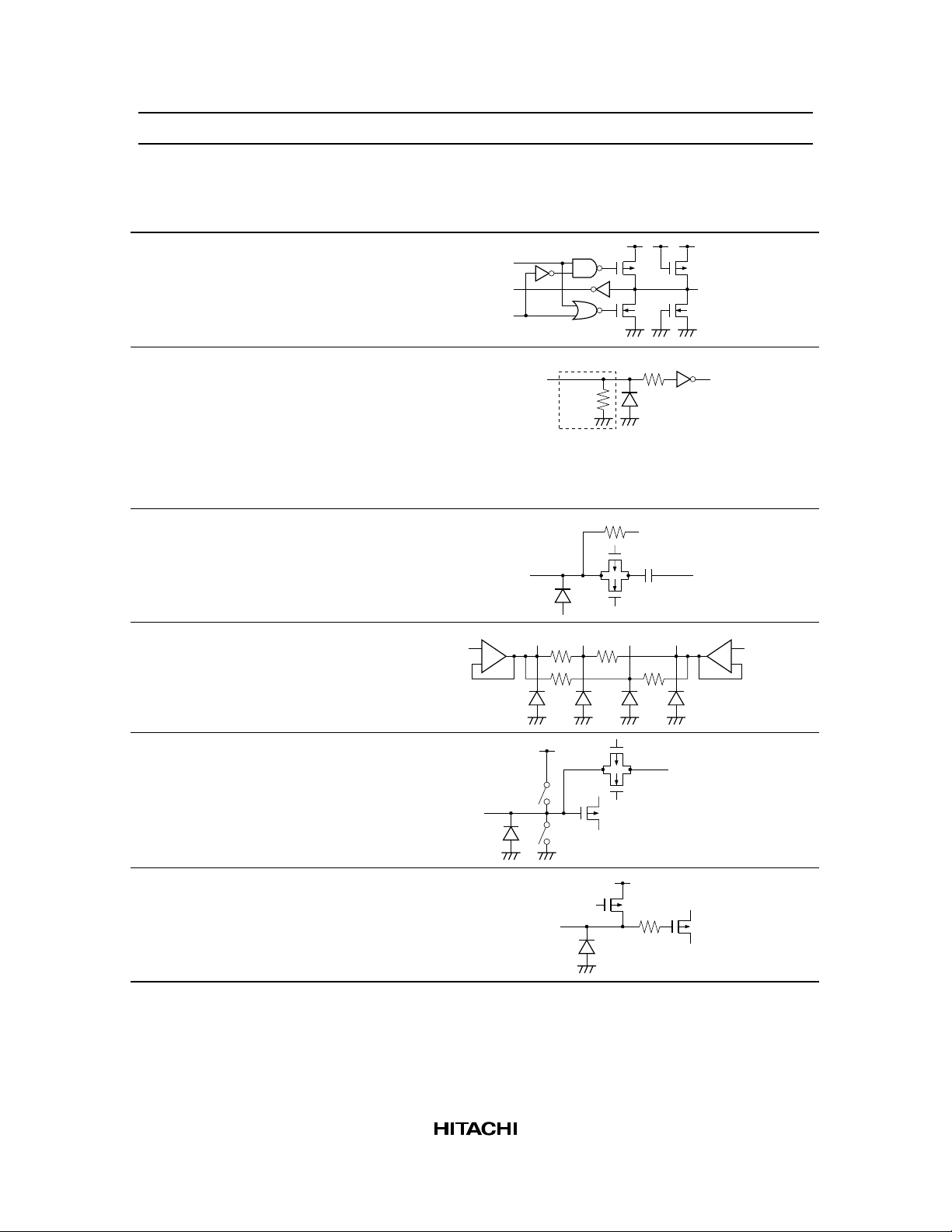
Input/Output Equivalent Circuit
Pin Name Equivalent Circuit
Digital output D0 to D9
DIN
STBY
or
OE
HD49323AF-01
DV
DD
Digital
output
Digital input ADCLK
OBP
SPBLK
SPSIG
CS
SCK
SDATA
PBLK
OE
Analog input CDSIN
Reference voltage input VRT
VRM
VRB
VRM2
Clamp CLP
Digital
input
CDSIN
VRT VRM VRM2
+
−
AV
DD
*1
70kΩ
(Typ)
Connected to
VRM internally
VRB
Connected to
VRM internally
+
−
Internal bias BIAS
Note: 1. Applies to OE and PBLK.
CLP
BIAS
AV
DD
5
Page 6
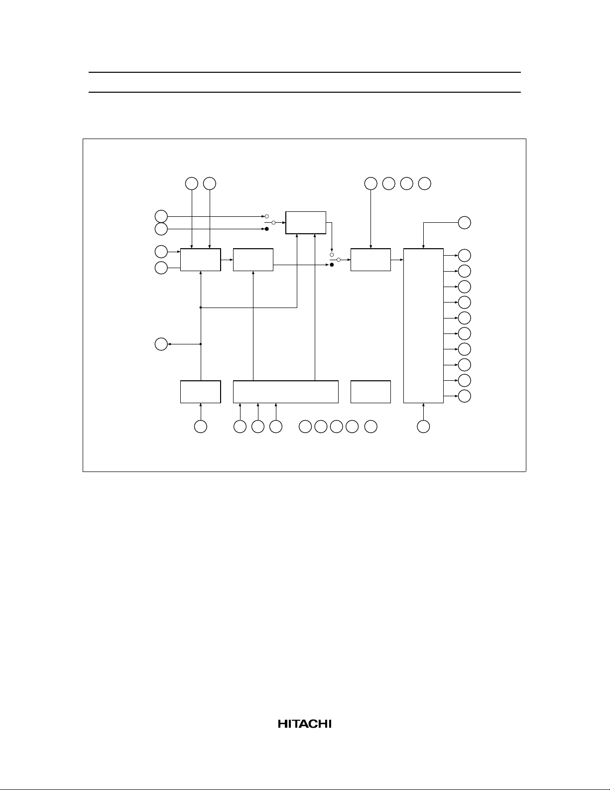
HD49323AF-01
Block Diagram
SPSIG
SPBLK
ADCLK
VRT
VRM
323334161918
VRB
TESTC
TESTY
CDSIN
VRM2
CLP
27
27
27
27
23
Gain
select
CDS AGC
Clamp
circuit
17 44 45 43 35
OBP
Serial interface
SCK
CS
SDATA
DD
AV
DD
DV
SS
AV
10bit
ADC
Bias
ganerator
SS
BIAS
DV
OE11
D9
11
D8
10
D7
9
D6
8
D5
7
D4
6
D3
5
Output latch circuit
17
PBLK
D2
4
D1
3
D0
2
6
Page 7
HD49323AF-01
Internal Functions
Functional Description
• CDS (Correlated Double Sampling) circuit
• AGC gain selection (11-bit digital control) *
AGC gain can be set in the range 0 dB to 34.7 dB on the (+) side, and –3.3 dB to 0 dB on the (–)
side by means of 11-bit serial data.
• Automatic offset adjustment is possible for the IC’s offsets (CDS, AGC, ADC) by means of serial data
control at power-on.*
1
• Digital output enable function
• Pre-blanking function
Digital output can be fixed at 32 LSB
• CDS offset cancel function
Note: 1. Serial data control
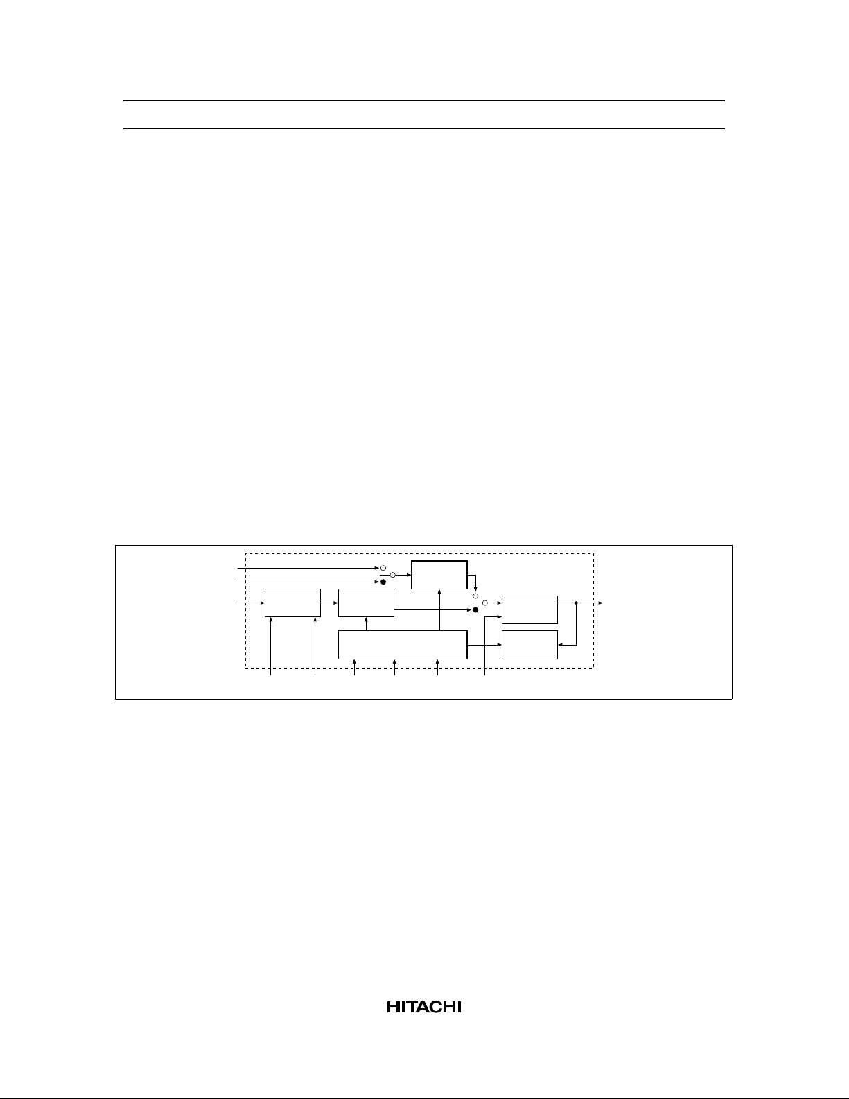
Operating Description
Figure 1 shows CDS/AGC +ADC function block.
1
TESTC
TESTY
CDSIN
CDS
SPBLK ADCLK
SPSIG SDATA
AGC
Serial interface
CS SCK
Gain
select
10bit
ADC
Offset
cancel
D0 to D9
Figure 1 CDS/AGC +ADC Function Block
1. CDS (Correlated Double Sampling) Circuit
The CCD imaging element alternately outputs a black level (A-period signal) and a signal including the
black level (B-period signal). The CDS circuit extracts the differential voltage between the black level
and the signal including the black level (see figure 4).
Black level sampling is performed at the rising edge of the SPBLK pulse, and signal level sampling is
performed at the rising edge of the SPSIG pulse. This sequence of operations extracts the differential
voltage between the black level and the signal including the black level, and supplies this to the nextstage AGC circuit.
2. Feed back clamp function
The clamp level is set by means of 5-bit serial data. The setting range is 32 LSB to 56 LSB, in 1 LSB
steps. A serial data value of 0 gives a 32 LSB setting, and a value of 24 gives a 56 LSB setting.
7
Page 8
HD49323AF-01
3. AGC Circuit
The AGC gain is set by means of 11-bit serial data. The setting range is –3.3 dB to 34.7 dB. Details of
the data are given in the following section.
The (–) side gain setting uses setting codes –81 to 0 in 0.0039-multiple steps, and the (+) side gain
setting uses setting codes 0 to 1023 in 0.034 dB steps.
• Detailed specifications of HD49323AF-01 AGC gain setting codes
(1) To improve S/N, the AD input dynamic range has been extended to 1.4 V from the 1.0 V of the
HD49322BF.
(2) There are two AGC gain ranges: (+) side 0 to 34.7 dB linear gain amp. (0.034 dB/step), and (–) side
0 to –3.3 dB “multiple” linear gain amp. (0.0039 multiple/step).
Range
CDS AGC ADC
Typ 1.4V
0V = 0 code
0.7V = 511 code
1.4V = 1023 code
OutputInput
Considering the case where AGC gain is set so that the ADC output code is 511 when a 150 mV signal is
input:
The HD49322BF AGC gain setting is (code 511)/150 mV multiple = 500 mV/150 mV multiple
The HD49323AF-01 AGC gain setting is (code 511)/150 mV multiple = 700 mV/150 mV multiple
Table 2 AGC Gain (−) Setting Code TableTable 1 AGC Gain (+) Setting Code Table
Code BIN (D10 to D0) dB
0 000 0000 0000 0.000
1 000 0000 0001 0.034
2 000 0000 0010 0.068
3 000 0000 0011 0.102
⋅
⋅
⋅
510 001 1111 1110 17.34
511 001 1111 1111 17.37
512 010 0000 0000 17.41
513 010 0000 0001 17.44
⋅
⋅
⋅
1020 011 1111 1100 34.68
1021 011 1111 1101 34.71
1022 011 1111 1110 34.75
1023 011 1111 1111 34.78
Code BIN (D10 to D0) Multiple
0 000 0000 0000 1.000
−1 111
−2 1111 1110 0.992
−3 111 1111 1101 0.988
⋅
⋅
⋅
−30 111 1110 0010 0.883
−31 111 1110 0001 0.879
−32 111 1110 0000 0.875
−33 111 1101 1111 0.871
⋅
⋅
⋅
−78 111 1011 0010 0.695
−79 111 1011 0001 0.691
−80 111 1011 0000 0.688
−81 111 1010 1111 0.684
1111 1111 0.996
111
dB
0.000
−0.034
−0.068
−0.102
−1.083
−1.121
−1.160
−1.199
−3.156
−3.205
−3.255
−3.304
4. Offset cancel circuit
When power is turned on, offset voltages generated by CDS, AGC, ADC, and other circuits by means
of serial data control are canceled. (Refer to page 24 (Operating Sequence at Power-On).)
8
Page 9
HD49323AF-01
5. Digital output enable function
When the OE pin is driven high, digital output goes to the high-Z state.
OE Pin Digital Output
High High-Z state
Low (or Open, GND) Output enable
6. Pre-blanking function
When the PBLK pin is driven high, digital output is fixed at 32 LSB. However, this is valid only when
the OE pin and serial data output mode settings (LINV, MINV, TEST, STBY) are low.
PBLK Pin Digital Output
High Fixed at 32 LSB
Low (or Open, GND) Active
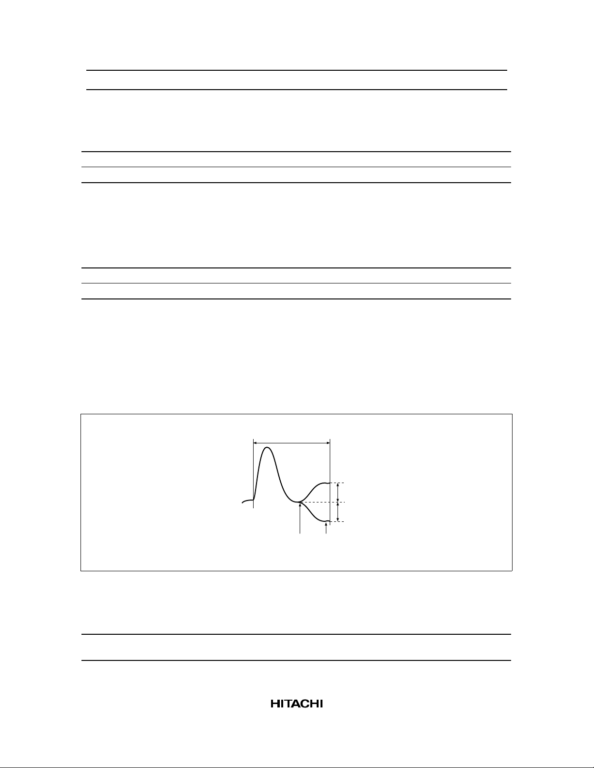
7. CCD offset cancel function
This function cancels the offset voltage (V
element. The definition of the CCD offset voltage (V
) during the optical black period of the CCD imaging
OFCCD
) is given below.
OFCCD
• The difference between the black level sampling voltage and signal level sampling voltage during the
OBP period is designated V
. This value is positive when (signal level sampling voltage) > (black
OFCCD
level sampling voltage).
Input signal for one pixel
(during OBP period)
CDS input
Black level
sampling
point
V
OFCCD
V
OFCCD
Signal level
sampling
point
(at +)
(at −)
Figure 2 Black Level Signal Level Difference during OBP Period
Table 3 Serial Data Settings
V
Cancel Function When Used When Not Used
OFCCD
Serial data settings VOFCON bit set to 1
VOFD0—3 (4 bits) set
VOFCON bit cleared to 0
9
Page 10

HD49323AF-01
• Determining serial set data VOFD0—3
(1) Provisional setting
Serial data VOFD0—3 settings are made according to the value of V
(2) Actual setting
The set data is adjusted so that the CLP pin (pin 23) voltage is closest to 1/2 AVDD when AGC gain
is set to the maximum.
The data obtained in (2) is used as the serial set data.
as shown in table 4.
OFCCD
Table 4 V
V
OFCCD
(mV) VOFD3 VOFD2 VOFD1 VOFD0
–110 0 0 1 0
–900011
–700100
–500101
–300110
–100111
+101000
+301001
+501010
+701011
+901100
+110 1 1 0 1
Serial Setting Data Correspondence Table (For Reference)
OFCCD
Serial Setting Data
10
Page 11

Timing Chart
Figure 3 shows the output timing.
• Sampling timing chart
0123456
HD49323AF-01
CDSIN
SPBLK
SPSIG
ADCLK
D0 to D9
N+1 N+2 N+3 N+4 N+5 N+6N
N−4N−5N−3N−2N−1N
Figure 3 Output Timing
• The ADC output signals (D0 to D9) are output at the rising edge of ADCLK.
• The pipeline delay is 5 clocks.
• Regarding OBP
OBP > 12fs
Note: The phase of OBP is for a low setting of the serial data OBP INV bit.
H period
11
Page 12

HD49323AF-01
Details of Timing Specifications
Details of Timing Specifications
Details of the timing specifications are shown in figure 4, and the timing specifications are summarized in
table 5.
• Serial data SP INV bit "Lo" setting
A period
B period
CDS input
(1)
(2) (3)
SPBLK 1.4V
SPSIG
ADCLK
1.4V
(7)
1.4V
• Serial data SP INV bit "Hi" setting
A period
CDS input
(1)
(2)
SPBLK 1.4V
(6)-1 (6)-2
SPSIG 1.4V
(7) (8)
ADCLK 1.4V
Figure 4 Details of Timing Specifications
(5)
B period
(5)
(4)
(4)
(6)-2(6)-1
(8)
(3)
12
Page 13

HD49323AF-01
Table 5 Each Timing Specifications
No. Timing Symbol Min Typ Max Unit Note
(1) Black level signal read-in time t
(2) SPBLK “Lo” period t
(3) Signal level read-in time t
(4) SPSIG “Lo” period t
(5) SPBLK rise to SPSIG rise t
(6)-1 ADCLK rise to SPBLK rise t
(6)-2 SPSIG rise to ADCLK rise t
(7), (8) ADCLK tWH Min / tWL Min t
CDS1
CDS2
CDS3
CDS4
CDS5
CDS6-1
CDS6-2
CDS7, 8
Note: 1. Negative when data before the rising edge of SPBLK/SPSIG is sampled, and positive when data
after the rising edge is sampled.
2. The polarity of SPBLK and SPSIG is for a low setting of the serial data SP INV bit.
+
−
SPBLK
SPSIG
1.4V
0510ns1
11 1/4f
ADCLK
Typ × 1.2 ns 2
0510ns1
11 1/4f
20 1/2f
ADCLK
ADCLK
Typ × 1.2 ns 2
Typ × 1.15 ns 2
25 — — ns 2
0ns2
22 ns
Detailed Timing Specifications for Digital Output Enable Control
Detailed timing specifications in the case of digital output enable control are shown in figure 5. When the
OE pin is high, output disable mode is entered and output goes to the high-Z state.
tLZ, t
OE
Digital output
(D0 to D9)
DV
DD
1.4V ×
3.0V
DV
DD
/2
DV
DD
V
V
DV
OL
OH
SS
t
LZ
t
HZ
t
ZL
/2
DV
DD
t
ZH
measurement load
measurement load
DV
ZL
DV
DD
2kΩ
10pF
DV
SS
t
, t
HZ
ZH
10pF 2kΩ
DV
SS
SS
Figure 5 Detailed Timing Specifications for Digital Output Enable Control
13
Page 14

HD49323AF-01
Detailed Timing Specifications for Pre-Blanking
Detailed timing specifications for pre-blanking are shown in figure 6. When the PBLK pin is high, digital
output is fixed at 32 LSB. However, the OE pin and serial data output mode settings (LINV, MINV,
TEST, STBY) take precedence.
DV
PBLK
1.4V ×
V
OH
DD
3.0V
Digital output
(D0 to D9)
t
PBLK
t
PBLK
Figure 6 Detailed Timing Specifications for Pre-Blanking
V
OL
14
Page 15

HD49323AF-01
Output Code Table
Table 6 Function Table
Digital Output
OEHSTBY
L
Note: 1. STBY, TEST, LINV, and MINV mode setting is performed by means of serial data.
TEST
X
X
H Hi-ZXXXX
L
L
H
2. OE and PBLK mode setting is performed by means of external input pins.
3. Pre-blanking mode is enabled when the PBLK pin is high and all other pins are low.
LINV
X
MINV
X
Hi-Z
X
In the table 7 below, D9 is inverted
LHL
In the table 7 below, D8 to D0 are inverted
LLH
In the table 7 below, D9 to D0 are inverted
LHH
D6D7D8D9PBLK
Operation Mode
D0D1D2D3D4D5
Output Hi-Z
Low power standby
Normal operationTable 7 as followsLLL
LLLLLHLLLLHLL
Pre-blanking
Test mode
HLHLHLHLHLXLL
HLHLHLHLHHXHL
LHLHLHLHLLXLH
LHLHLHLHLHXHH
Table 7 Output Code Table
511
512
1020
1021
1022
1023
……
0
1
2
3
……
Output
code
Step
……
……
……
……
……
……
……
……
Input LevelOutput Pin
D0D1D2D3D4D5D6D7D8D9
LLLLLLLLLL
→0V
HLLLLLLLLL
LHLLLLLLLL
HHLLLLLLLL
……
→0.7V
HHHHHHHHHL
LLLLLLLLLH
LLHHHHHHHH
HLHHHHHHHH
LHHHHHHHHH
H
→1.4VHHHHHHHHH
15
Page 16

HD49323AF-01
Absolute Maximum Ratings (Ta = 25°C)
Item Symbol Ratings Unit
Power supply voltage V
Power dissipation P
Analog input voltage V
Digital input voltage V
DD(max)
D(max)
IN(max)
I(max)
Operating temperature Topr –10 to +85 °C
Storage temperature Tstg –55 to +125 °C
Note: 1. VDD indicates AVDD and DVDD.
2. Common connection of AV
and DVDD should be made off-chip. If AVDD and DVDD are isolated
DD
by a noise filter, the phase difference should be 0.3 V or less at power-on and 0.1 V or less
during operation.
6.0 V
400 mW
–0.3 to AVDD +0.3 V
–0.3 to 6.0 V
16
Page 17

HD49323AF-01
Electrical Characteristics (Unless othewide specified, Ta = 25°C, AVDD = 3.0 V,
DVDD = 3.0 V, R
Item Symbol Min Typ Max Unit Test Conditions Remarks
Power supply
voltage range
Conversion f
frequency f
Digital input voltage V
Digital output V
voltage V
Digital input current I
Digital output I
current I
ADC resolution RES 10 10 10 bit
ADC integration
linearity error
ADC differentiation DNL+ — 0.3 0.8 LSB f
linearity error DNL– –0.8 –0.3 — LSB
Digital output delay
time
Digital output
hold time
Note: 1. DNL calculate the difference of linearity error between next two codes.
= 24 kΩ)
EXT
V
DD
max 20 — — MHz
CLK
min — — 5.5 MHz
CLK
IH
V
IL
V
IH2
V
IL2
OH
OL
IH
I
IH2
I
IL
OZH
OZL
2.70 3.00 3.60 V f
DV
2.0 ×
0—
DV
2.25 ×
0—
— 5.0 V 5 V
DD
3.0
DV
0.8 ×
— 5.0 V 5 V
DD
3.0
DV
0.6 ×
V Digital
DD
3.0
V CS, SCK,
DD
3.0
DVDD –0.5 — — V IOH = –2 mA
— — 0.5 V IOL = +2 mA
——50µAV
— — 250 µAV
–50 — — µAV
——50µAV
–50 — — µAV
INL — 4 10 LSBp-p f
t
PD
t
HOLD
— — 35 ns CL = 10 pF
10 — — ns
= 20 MHz
CLK
amplitude
input
possible
input pins
except CS,
SCK, and
SDATA
amplitude
input
possible
SDATA
= 5.0 V Digital
IH
input pins
except
PBLK and
OE
= 5.0 V PBLK, OE
IH
= 0 V
IL
= V
OH
DD
= 0 V
OL
= 20 MHz
CLK
= 20 MHz *1
CLK
17
Page 18

HD49323AF-01
C
Electrical Characteristics (Unless othewide specified, Ta = 25°C, AVDD = 3.0 V,
DVDD = 3.0 V, R
Item Symbol Min Typ Max Unit Test Conditions Remarks
Sleep current I
Standby current I
ADC Input range V
Digital output Hi-Z t
delay time t
Digital output PBLK delay
time
Quiescent current I
Timing specification (1) t
Timing specification (2) t
Timing specification (3) t
Timing specification (4) t
Timing specification (5) t
Timing specification (6-1) t
Timing specification (6-2) t
Timing specification (7) t
Timing specification (8) t
Input current IIN
Clamp level CLP(00) — (32) — LSB *2
Note: 2. Items in parentheses are reference values.
3. Refer to page 12 (Details of Timing Specifications).
4. This is not transition current, but static current.
= 24 kΩ) (cont)
EXT
SLP
STBY
INp-p
HZ
LZ
t
ZH
t
ZL
t
PBLK
DD1
CDS1
CDS2
CDS3
CDS4
CDS5
CDS6-1
CDS6-2
CDS7
CDS8
CDS
–100 0 100 µA Digital input pins
— 8 12 mA Digital input pins
— (1.4) — V *2
— — 100 ns RL = 2 kΩ *3
— — 100 ns CL = 10 pF
— — 100 ns
— — 100 ns
— — 100 ns CL = 10 pF *3
—6678 mAf
0 5 10 ns *3
11 1/4f
ADCLK
Typ × 1.2 ns
0 5 10 ns
11 1/4f
20 1/2f
ADCLK
ADCLK
Typ × 1.2 ns
Typ × 1.15 ns
25 — — ns
0——ns
22 — — ns
22 — — ns
–60 — 10 µAf
CLP(16) — (48) — LSB
CLP(24) — (56) — LSB
fixed at 0 V,
output pins open
fixed at 0 V
= 20 MHz CDSIN
CLK
= 20 MHz,
LK
Black/signal level
difference = 1 V,
gain = 0 dB
use
*4
18
Page 19

HD49323AF-01
Electrical Characteristics (Unless othewide specified, Ta = 25°C, AVDD = 3.0 V,
DVDD = 3.0 V, R
Item Symbol Min Typ Max Unit Test Conditions Remarks
AGC gain(–) AGC(–081) –5.3 –3.3 –1.3 dB
AGC gain(+) AGC(0000) –2.0 0 2.0 dB
= 24 kΩ) (cont)
EXT
AGC(0000) –2.0 0 2.0 dB
AGC(0128) 2.4 4.4 6.4 dB
AGC(0256) 6.7 8.7 10.7 dB
AGC(0384) 11.1 13.1 15.1 dB
AGC(0512) 15.4 17.4 19.4 dB
AGC(0640) 19.8 21.8 23.8 dB
AGC(0768) 24.1 26.1 28.1 dB
AGC(0896) 28.5 30.5 32.5 dB
AGC(1023) 32.3 34.8 37.8 dB
19
Page 20

HD49323AF-01
Serial Interface Specification
SDATA latched
CS
at rise of SCK *1
t
1
INT
f
SCK
t
INT
2
*2, 3
SCK
SDATA
Note: 1.
t
su
DI00DI
t
ho
DI02DI03DI04DI05DI06DI07DI08DI09DI10DI11DI12DI13DI14DI
01
SDATA is latched at the rise of SCK.
2.
Input 16 SCK clocks while CS is low. If the number of clocks is more or less than 16,
the data will be invalid.
3.
If data transmission is aborted, the data is invalid.
Figure 7 Serial Interface Specification
Data fixed
at rise of CS
15
20
Page 21

Table 8 Serial Data Functions Table
DI 00
(LSB)
HD49323AF-01
Resister 2Resister 0 Resister 3Resister 1
Hi
LoLo
Hi
DI 01 Hi
DI 02
DI 03
DI 04
DI 05
DI 06
DI 07
DI 08
DI 09
DI 10
DI 11
DI 12
DI 13
DI 14
(MSB)
DI 15
Notes:1.
AGC Gain setting (LSB)
AGC Gain setting
AGC Gain setting
AGC Gain setting
AGC Gain setting
AGC Gain setting
AGC Gain setting
AGC Gain setting
AGC Gain setting
AGC Gain setting
AGC Gain setting (MSB)
Test mode Low setting *
Test mode Low setting *
Output mode setting (STBY) *
STBY: Reference voltage generation circuit is in the operational state.
SP INV SPSIG/SPBLK
inversion
OBP INV
CIF
VOFCON
VOFD0 (LSB)
CCD offset voltage setting
VOFD1
CCD offset voltage setting
VOFD2
CCD offset voltage setting
VOFD3 (MSB)
CCD offset voltage setting
Output mode setting (LINV)
Output mode setting (MINV)
Output mode setting (TEST)
2
RESET
2
OFRST
1
SLP
Lo
Lo→Negative input
Hi→Positive input
CLK
CLK
>10MHz
<10MHz
3
1
Lo→f
Hi→f
Lo→OFF *
Hi→ON
Lo→Reset mode
Hi→Normal operation mode
Lo→Normal operation mode
Hi→Offset cancel mode
Lo→Normal operation mode *
Hi→Sleep mode
Clamp level adjustment (LSB)
Clamp level adjustment
Clamp level adjustment
Clamp level adjustment
Clamp level adjustment (MSB)
SLP: All circuits are in the sleep state.
Test mode is used for IC testing, and so cannot be used.
2.
Register 2 test mode should be set in accordance with the specification at the right of the column.
For other registers, the setting should only be made in the all-low state.
Setting of VOFCON
3.
: Lo→CCD offset cancel function OFF
: Hi→CCD offset cancel function ON
Timing Specifications
Min
f
SCK
t
INT
t
su
t
ho
1, 2
50ns
50ns
50ns
• OBP polarity
OBP INV setting = Lo
Max
3MHz
H period
OBP > 12fs
Negative
HiLo
2
LowTest mode *
Low
Low
Low
High
Low
High
High
High
Test mode *
Use prohibited
ALL Low
2
OBP INV setting = Hi
Positive
H period
OBP > 12fs
21
Page 22

HD49323AF-01
Notice for Use
1. Careful handling is necessary to prevent damage due to static electricity.
2. This product has been developed for consumer applications, and should not be used in non-consumer
applications.
3. As this IC is sensitive to power line noise, the ground impedance should be kept as small as possible.
Also, to prevent latchup, a ceramic capacitor of 0.1 µF or more and an electrolytic capacitor of 10 µF or
more should be inserted between the ground and power supply.
4. Common connection of AVDD and DVDD should be made off-chip. If AVDD and DVDD are isolated by a
noise filter, the phase difference should be 0.3 V or less at power-on and 0.1 V or less during operation.
5. If a noise filter is necessary, make a common connection after passage through the filter, as shown in
the figure below.
Analog
+3.0V
Noise filter
AV
DD
HD49323AF-01
AV
SS
DV
DV
DD
SS
Digital
+3.0V
Noise filter Example of noise filter
DV
DD
HD49323AF-01
DV
SS
AV
AV
DD
0.01µF
SS
100µH
0.01µF
6. Connect AVSS and DVSS off-chip using a common ground. If there are separate analog system and
digital system set grounds, connect to the analog system.
7. When VDD is specified in the delivery specification, this indicates AVDD and DVDD.
8. No Connection (NC) pins are not connected inside the IC, but it is recommended that they be used as
power supply ground pins or left open to prevent crosstalk in adjacent analog pins.
9. To ensure low thermal resistance of the package, a Cu-type lead material is used. As this material is
less tolerant of bending than Fe-type lead material, careful handling is necessary.
10.The infrared reflow soldering method should be used to mount the chip. Note that general heating
methods such as solder dipping cannot be used.
11.Depending on the mounting state, picture quality (crosscut noise, wave pattern, etc.) will be dependent
upon the timing of the SPBLK, SPSIG, and ADCLK signals. Check the mounting state thoroughly
before use.
12.Serial communication should not be performed during the effective video period, since this will result in
degraded picture quality. Also, use of dedicated ports is recommended for the SCK and SDATA
signals used in the HD49323AF-01. If ports are to be shared with another IC, picture quality should
first be thoroughly checked.
13.At power-on, automatic adjustment of the offset voltage generated from CDS, AGC, ADC, etc., must be
implemented in accordance with the power-on operating sequence (see page 24).
22
Page 23

HD49323AF-01
14.If the phase difference between the black level sampling voltage and the signal level sampling voltage
during the CCD imaging element optical black period (the CCD offset voltage) is ±30 mV or greater,
the CCD offset cancel function (page 9, item 7, CCD Offset Cancel Function) must be implemented.
The CCD offset voltage variation after implementation of the CCD offset cancel function should be
within ±20 mV.
15.The CDSIN pin is clamped at VRM (≅ AVDD/2) during operation. The IC may suffer permanent
damage if used with a pin voltage in the range –0.3 V to AVDD + 0.3 V. Careful attention must
therefore be paid to the input signals.
23
Page 24

HD49323AF-01
Operating Sequence at Power-On
V
DD
Must be stabilized within operating
power supply voltage range
0ms
0ms
0ms
or
more
or
more
1V(16ms)
or more
or
more
4V(64ms)
or more
0ms
or
more
TG and
Camera DSP
control start
RESET
OFRST
HD49323AF
data transfer
SPBLK
SPSIG
ADCLK
OBP
etc.
Note:
RESET and OFRST both use serial data transmission.
1.
Stable input of SPBLK, SPSIG, ADCLK, and OBP is assumed before RESET is transmitted.
2.
Numbers in parentheses in the figure show the order of transfer.
3.
(1) RESET = "Lo"
0ms
or more
(2) RESET = "Hi"
(4) OFRST = "Hi"
(3) Data transfer
(5) OFRST = "Lo"
(6) Data
transfer
Figure 8 Operating Sequence at Power-On
Serial data transmission contents are shown in table 9.
“X” indicates data for which the clock polarity, clamp level, etc., can be selected. See page 21 (table 8,
Serial Data Functions Table) for the purpose of the data.
Table 9 Serial Data
Order of Transfer
(1) RESET = "Lo"
(2) RESET = "Hi"
(3) Data transfer
Wait
(4) OFRST = "Hi"
Wait
(5) OFRST = "Lo"
(6) Data transfer
24
b)
c)
d)
Serial Data (DI)MSB LSB
101112131415
000000a)
000100
000100
010111
000110e)
000100g)f)
XXXXX0
Remarks
00010203040506070809
1000000000
1000000000
10XXXXXXXX
01XXXXX000
1 V (16 ms) or more
10XXXXXXXX
4 V (64 ms) or more
10XXXXXXXX
00XXXXXXXX
Page 25

Example of Recommended External Circuit
HD49323AF-01
• CDS/AGC function is used
(OE control and pre-blanking function are not used)
C4
C5
15p
15pC315pC215pC10.1
SS
DD
AV
AV
HA49323AF-01
(CDS/AGC/ADC)
C19
0.1
from
CCD
out
Analog
−
+
C9
1/16
C12 0.1
C13 0.1
C14 0.1
C15 0.1
3.0V
C8
0.1
R5
24k
L1
47µ
25
26
27
28
29
30
31
32
33
34
35
36
C17
47/6
C7
C6
1.0
0.1
23
212224
NC
CLP
VRM2
AV
SS
AV
DD
CDSIN
TESTY
TESTC
AV
SS
AV
DD
VRB
VRM
VRT
BIAS
NC
AVSSAVDDNCNCAVDDAVSSCS
38 45 46 47 4844434241403937
C18
0.1
SPSIG
SPBLK
16 15 14 1317181920
OBP
SCK
DD
DV
ADCLK
SDATA
DVDDDVSSDV
C20
0.1
R1 220
R2 220
R3 220
R4 220
SS
OE
DV
NC
12
11
D9
10
D8
9
D7
8
D6
7
D5
6
D4
5
D3
4
D2
3
D1
2
D0
1
PBLK
SS
C21
47/6
Serial data input
from
Timing generator
to
Camera
signal
processor
L2
47µ
Digital
3.0V
GND
25
Page 26

HD49323AF-01
Package Dimensions
Preliminary
9.0 ± 0.2
7.0
36 25
37
9.0 ± 0.2
48
112
*0.21 ± 0.05
0.19 ± 0.04
0.75 0.75
0.10
*Dimension including the plating thickness
Base material dimension
24
13
0.08
M
1.40
+0.09
−0.05
0.13
0.5
1.70 Max
0.15 ± 0.04
*0.17 ± 0.05
0.50 ± 0.10
Hitachi Code
JEDEC
EIAJ
Weight
1.00
0° − 8°
(reference value)
Unit: mm
FP-48C
Conforms
0.2 g
26
Page 27

HD49323AF-01
Cautions
1. Hitachi neither warrants nor grants licenses of any rights of Hitachi’s or any third party’s patent,
copyright, trademark, or other intellectual property rights for information contained in this document.
Hitachi bears no responsibility for problems that may arise with third party’s rights, including
intellectual property rights, in connection with use of the information contained in this document.
2. Products and product specifications may be subject to change without notice. Confirm that you have
received the latest product standards or specifications before final design, purchase or use.
3. Hitachi makes every attempt to ensure that its products are of high quality and reliability. However,
contact Hitachi’s sales office before using the product in an application that demands especially high
quality and reliability or where its failure or malfunction may directly threaten human life or cause risk
of bodily injury, such as aerospace, aeronautics, nuclear power, combustion control, transportation,
traffic, safety equipment or medical equipment for life support.
4. Design your application so that the product is used within the ranges guaranteed by Hitachi particularly
for maximum rating, operating supply voltage range, heat radiation characteristics, installation
conditions and other characteristics. Hitachi bears no responsibility for failure or damage when used
beyond the guaranteed ranges. Even within the guaranteed ranges, consider normally foreseeable
failure rates or failure modes in semiconductor devices and employ systemic measures such as failsafes, so that the equipment incorporating Hitachi product does not cause bodily injury, fire or other
consequential damage due to operation of the Hitachi product.
5. This product is not designed to be radiation resistant.
6. No one is permitted to reproduce or duplicate, in any form, the whole or part of this document without
written approval from Hitachi.
7. Contact Hitachi’s sales office for any questions regarding this document or Hitachi semiconductor
products.
Hitachi, Ltd.
Semiconductor & Integrated Circuits.
Nippon Bldg., 2-6-2, Ohte-machi, Chiyoda-ku, Tokyo 100-0004, Japan
Tel: Tokyo (03) 3270-2111 Fax: (03) 3270-5109
URL NorthAmerica : http:semiconductor.hitachi.com/
For further information write to:
Hitachi Semiconductor
(America) Inc.
179 East Tasman Drive,
San Jose,CA 95134
Tel: <1> (408) 433-1990
Fax: <1>(408) 433-0223
Europe : http://www.hitachi-eu.com/hel/ecg
Asia (Singapore) : http://www.has.hitachi.com.sg/grp3/sicd/index.htm
Asia (Taiwan) : http://www.hitachi.com.tw/E/Product/SICD_Frame.htm
Asia (HongKong) : http://www.hitachi.com.hk/eng/bo/grp3/index.htm
Japan : http://www.hitachi.co.jp/Sicd/indx.htm
Hitachi Europe GmbH
Electronic components Group
Dornacher Straße 3
D-85622 Feldkirchen, Munich
Germany
Tel: <49> (89) 9 9180-0
Fax: <49> (89) 9 29 30 00
Hitachi Europe Ltd.
Electronic Components Group.
Whitebrook Park
Lower Cookham Road
Maidenhead
Berkshire SL6 8YA, United Kingdom
Tel: <44> (1628) 585000
Fax: <44> (1628) 778322
Hitachi Asia Pte. Ltd.
16 Collyer Quay #20-00
Hitachi Tower
Singapore 049318
Tel: 535-2100
Fax: 535-1533
Hitachi Asia Ltd.
Taipei Branch Office
3F, Hung Kuo Building. No.167,
Tun-Hwa North Road, Taipei (105)
Tel: <886> (2) 2718-3666
Fax: <886> (2) 2718-8180
Copyright © Hitachi, Ltd., 1998. All rights reserved. Printed in Japan.
Hitachi Asia (Hong Kong) Ltd.
Group III (Electronic Components)
7/F., North Tower, World Finance Centre,
Harbour City, Canton Road, Tsim Sha Tsui,
Kowloon, Hong Kong
Tel: <852> (2) 735 9218
Fax: <852> (2) 730 0281
Telex: 40815 HITEC HX
27
 Loading...