

Page 1
HD-4702
March 1997
Features
• HD-4702 Provides 13 Commonly Used Bit Rates
• Uses a 2.4576MHz Crystal/Input for Standard
Frequency Output (16 Times Bit Rate)
• Low Power Dissipation
• Conforms to EIA RS-404
• One HD-4702 Controls up to Eight Transmission
Channels
• Initialization Circuit Facilitates Diagnostic Fault
Isolation
• On-Chip Input Pull-Up Circuit
Ordering Information
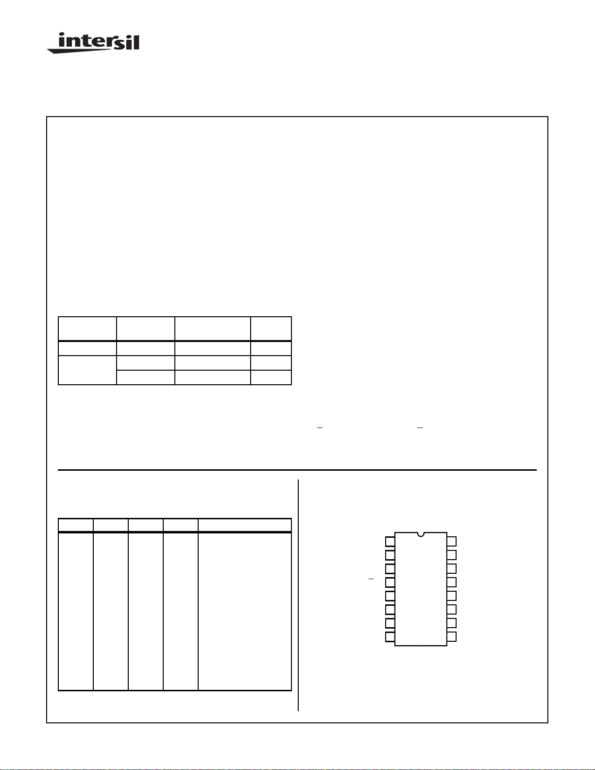
TEMP.
PACKAGE
PDIP -40 to +85 HD3-4702-9 E16.3
CERDIP -40 to +85 HD1-4702-9 F16.3
SMD# -55 to +125 5962-9051801MEA F16.3
RANGE (oC) PART NUMBER PKG. NO.
CMOS Programmable Bit Rate Generator
Description
The HD-4702 Bit Rate Generator provides the necessary clock
signals for digital data transmission systems, such as a UART. It
generates 13 commonly used bit rates using an on-chip crystal
oscillator or an external input. For conventional operation generating 16 output clock pulses per bit period, the input clock frequency must be 2.4576MHz (i.e. 9600 Baud x 16 x 16, since
there is an internal ÷ 16 prescaler). A lower input frequency will
result in a proportionally lower output frequency.
The HD-4702 can provide multi-channel operation with a minimum of external logic by having the clock frequency CO and the
÷ 8 prescaler outputs Q0, Q1, Q2 available externally. All signals
have a 50% duty cycle except 1800 Baud, which has less than
0.39% distortion.
The four rate select inputs (S0-S3) select which bit rate is at the
output (Z). See Truth Table for Rate Select Inputs for select code
and output bit rate. Two of the 16 select codes for the HD-4702 do
not select an internally generated frequency, but select an input
into which the user can feed either a different frequency, or a static
level (High or Low) to gener ate “ZERO BAUD”.
The bit rates most commonly used in modern data terminals
(110, 150, 300, 1200, 2400 Baud) require that no more than one
input be grounded for the HD-4702, which is easily achieved with
a single 5-position switch.
The HD-4702 has an initialization circuit which generates a master reset for the scan counter. This signal is derived from a digital
differentiator that senses the first high level on the CP input after
ECP input goes low. When ECP is high, selecting the crystal
the
input, CP must be low. A high level on CP would apply a continuous reset. See Clock Modes and Initialization below .
Truth Table Pinout
TRUTH TABLE FOR RATE SELECT INPUTS
(Using 2.4576MHz Crystal)
S3 S2 S1 S0 OUTPUT RATE (Z)
L
L
L
L
L
L
L
L
H
H
H
H
H
H
H
H
NOTE: 19200 Baud by connecting Q2 to IM.
CAUTION: These devices are sensitive to electrostatic discharge; follow proper IC Handling Procedures.
http://www.intersil.com or 407-727-9207
L
L
L
L
H
H
H
H
L
L
L
L
H
H
H
H
L
L
H
H
L
L
H
H
L
L
H
H
L
L
H
H
L
MUX Input (IM)
H
MUX Input (IM)
L
50 Baud
H
75 Baud
L
134.5 Baud
H
200 Baud
L
600 Baud
H
2400 Baud
L
9600 Baud
H
4800 Baud
L
1800 Baud
H
1200 Baud
L
2400 Baud
H
300 Baud
L
150 Baud
H
110 Baud
| Copyright © Intersil Corporation 1999
5-1
HD-4702 (CERDIP, PDIP)
TOP VIEW
1
Q0
2
Q1
3
Q2
4
E
CP
5
CP
6
O
X
I
7
X
8
GND
16
V
CC
15
I
M
14
S0
13
S1
12
S2
S3
11
10
Z
9
CO
File Number 2954.1
Page 2
HD-4702
Pin Description
PIN NUMBER TYPE SYMBOL DESCRIPTION
16 V
8 GND GROUND
5 I CP EXTERNAL CLOCK INPUT
4IE
7II
6OO
15 I I
11, 12, 13, 14 I S0 - S3 BAUD RATE SELECT INPUTS
9 O CO CLOCK OUTPUT
1, 2, 3 O Q0 - Q
10 O Z BIT RATE OUTPUT
CLOCK MODES AND INITIALIZATION
IX E
X L Clocked from CP
CP
H L Clocked from I
CP OPERATION
CC
CP
X
X
M
VCC: Is the +5V power supply pin. A 0.1µF capacitor between pins 16 and 8 is
recommended for decoupling.
EXTERNAL CLOCK ENABLE: A low signal on this input allows the baud rate to be
generated from the CP input.
CRYSTAL INPUT
CRYSTAL DRIVE OUTPUT
MULTIPLEXED INPUT
SCAN COUNTER OUTPUTS
2
X
X H H Continuous Reset
X L Reset During 1st CP = High
Time
H = HIGH Level
L = LOW Level
X = Don’t Care
= Clock Pulse
= 1st HIGH Level Clock Pulse after ECP goes LOW
NOTE: Actual output frequency is 16 times the indicated Output
Rate, assuming a clock frequency of 2.4576MHz.
5-2
Page 3
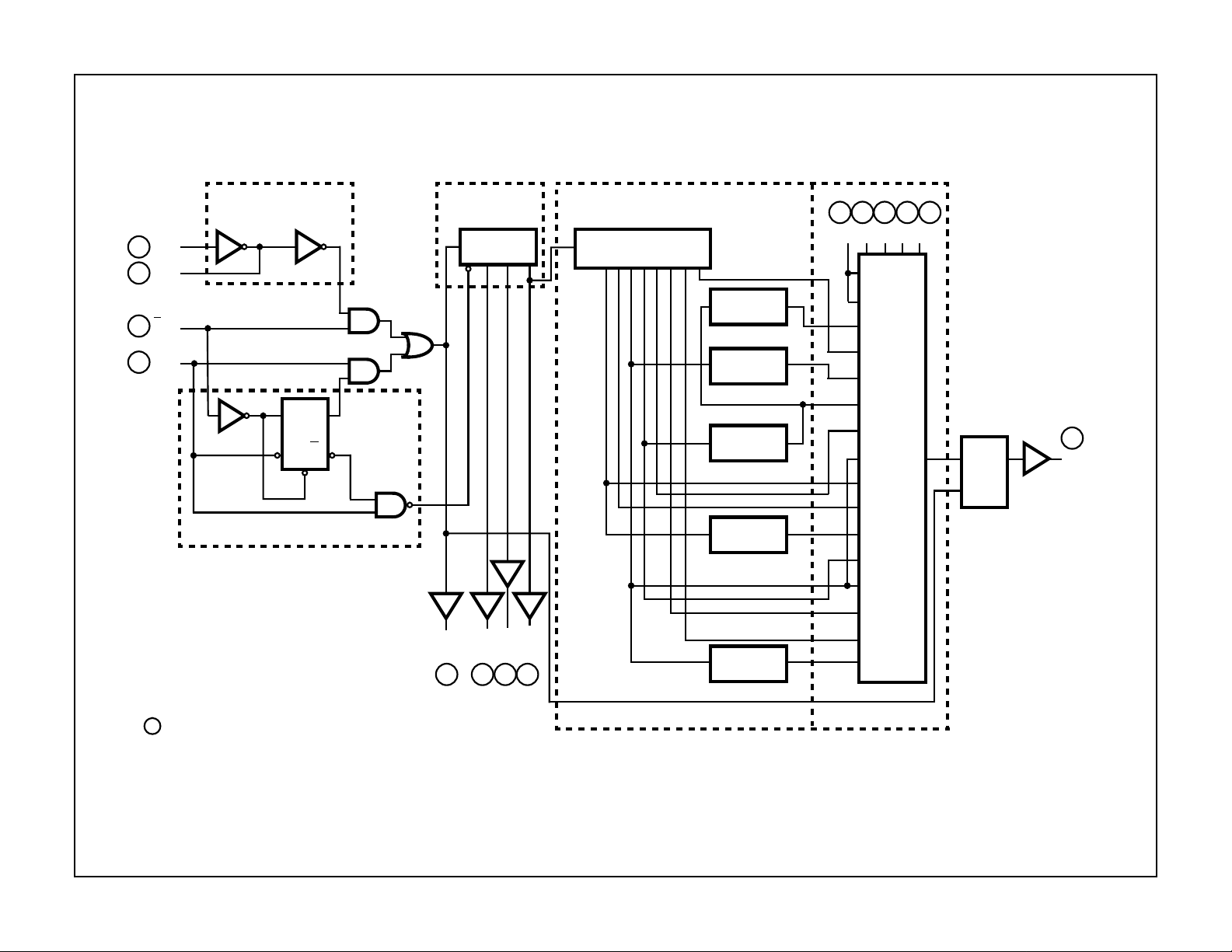
Block Diagram
5-3
MULTIPLEXER
14 13 12 11
15
I
S0 S1 S2 S3
M
0
1
2
3
4
5
6
7
8
9
10
11
12
13
14
15
50
75
134.5
200
600
2400
9600
4800
1800
1200
2400
300
150
110
DQ
FF
CP
MR
10
Z
HD-4702
CIRCUIT
OSCILLATOR
CIRCUIT
DQ
FF
CP Q
MR
MR
CO
9
SCAN
COUNTER
CP 8
÷
MR
Q0Q1Q
1 2 3
COUNTER NETWORK
CP
MR
9600
4800
2400
1200
600
300
150
75
CP 4÷Q
CP 18÷Q
CP 6÷Q
CP 16/3÷Q
2
CP 22÷Q
MR
MR
MR
MR
MR
(NOTE)
I
7
X
O
6
X
E
CP
4
5
CP
INITIALIZATION
=
PIN 16V
DD
V
PIN 8
=
SS
=
PIN NUMBER
NOTE: See Figure 4 in Design Information for Crystal Specifications.
Page 4

HD-4702
Application Information
Single Channel Bit Rate Generator
Figure 1 shows the simplest application of the HD-4702. This
circuit generates one of five possible bit rates asdetermined by
the setting of a single pole, 5-position switch. The Bit Rate Output (Z) drives one standard TTL load or four low pow er Schottky
loads over the full temperature range. The possible output frequencies correspond to 110, 150, 300, 1200, and 2400 Baud.
For many low cost terminals, these five bit r ates are adequate .
56pF
56pF
2.4576 MHz
CRYSTAL
† See Table 1.
10M
1
2
IMS0 S1 S2 S3
C
P
E
CP
I
X
†
O
X
HD-4702
COQ0Q1Q2Z
SPST SWITCH
5
34
OUTPUT
Other bit rate combinations can be generated by changing the
Scan Counter to Selector interconnection or by inserting logic
gates into this path.
IMS0 S1 S2 S3
C
P
56pF
56pF
10M
2.4576 MHz
CRYSTAL
E
CP
I
X
†
O
X
A0
A1
CL Q0 Q1 Q2 Q3 Q4 Q5 Q6 Q7
A2
110
HD-4702
COQ0Q1Q2Z
E
93L34
4800
1800
1200
9600
2400
D
300
150
† See Table 1.
FIGURE 2. BIT RATE GENERATOR CONFIGURATION WITH
EIGHT SIMULTANEOUS FREQUENCIES
SWITCH POSITION HD-4702 BIT RATE
1 110 Baud
2 150 Baud
3 300 Baud
4 1200 Baud
5 2400 Baud
FIGURE 1. SWITCH SELECTABLE BIT RATE GENERATOR
CONFIGURATION PROVIDING FIVE BIT RATES
Simultaneous Generation of Several Bit Rates
Figure 2 shows a simple scheme that generates eight bit rates
on eight output lines, using one HD-4702 and one 93L34 Bit
Addressable Latch. This and the following applications take
advantage of the built-in scan counter (prescaler) outputs. As
shown in the block diagram, these outputs (Q
to Q2) go
0
through a complete sequence of eight states for every halfperiod of the highest output frequency (9600 Baud). Feeding
these Scan Counter Outputs back to the Select Inputs of the
multiplexer causes the HD-4702 to interrogate sequentially
eight different frequency signals. The 93L34 8-bit addressable
Latch, addressed by the same Scan Counter Outputs, re-converts the multiplexed single Output (Z) of the HD-4702 into
eight parallel output frequency signals. In the simple scheme of
Figure 2, input S3 is left open (HIGH) and the following bit rates
are generated:
Q0: 110 Baud Q1: 9600 Baud Q2: 4800 Baud
Q3: 1800 Baud Q4: 1200 Baud Q5: 2400 Baud
Q6: 300 Baud Q7: 150 Baud
19200 Baud Operation
Though a 19200 Baud signal is not internally routed to the multiplexer, the HD-4702 can be used to generate this bit rate by
connecting the Q
output to IM input and applying select code.
2
An additional 2-input NOR gate can be used to retain the “Zero
Baud” feature on select code 1 for the HD-4702 (See Figure 3).
IMS0 S1 S2 S3
C
P
56pF
56pF
10M
2.4576 MHz
CRYSTAL
E
CP
I
X
†
O
X
HD-4702
COQ0Q1Q2Z
OUTPUT
† See Table 1.
FIGURE 3. 19200 BAUD OPERATION
TABLE 1. CRYSTAL SPECIFICATIONS
PARAMETERS TYPICAL CRYSTAL SPEC
Frequency 2.4576MHz “AT” Cut
Series Resistance (Max) 250
Unwanted Modes -6.0dB (Min)
Type of Operation Parallel
Load Capacitance 32pF +0.5
5-4
Page 5

HD-4702
Absolute Maximum Ratings Thermal Information
Supply Voltage . . . . . . . . . . . . . . . . . . . . . . . . . . . . . . . . . . . . .+8.0V
Input, Output or I/O Voltage . . . . . . . . . . . GND -0.5V to VCC+0.5V
ESD Classification . . . . . . . . . . . . . . . . . . . . . . . . . . . . . . . . Class 1
Typical Derating Factor. . . . . . . . . . . . 1mA/MHz Increase in ICCOP
CAUTION: Stresses above those listed in “Absolute Maximum Ratings” may cause permanent damage to the device. This is a stress only rating and operation
of the device at these or any other conditions above those indicated in the operational sections of this specification is not implied.
Operating Conditions
Operating Voltage Range . . . . . . . . . . . . . . . . . . . . . +4.5V to +5.5V Operating Temperature Range
Thermal Resistance (Typical) θ
JA
θ
JC
CERDIP Package . . . . . . . . . . . . . . 78oC/W 23oC/W
PDIP Package. . . . . . . . . . . . . . . . . 90oC/W N/A
Storage Temperature Range. . . . . . . . . . . . . . . . . .-65oC to +150oC
Maximum Junction Temperature . . . . . . . . . . . . . . . . . . . . . . . . . . . .
Ceramic Package . . . . . . . . . . . . . . . . . . . . . . . . . . . . . . . +175oC
Plastic Package. . . . . . . . . . . . . . . . . . . . . . . . . . . . . . . . . +150oC
Maximum Lead Temperature (Soldering 10s) . . . . . . . . . . . .+300oC
Die Characteristics
Gate Count . . . . . . . . . . . . . . . . . . . . . . . . . . . . . . . . . . . .720 Gates
HD-4702-9. . . . . . . . . . . . . . . . . . . . . . . . . . . . . . .-40oC to +85oC
HD-4702-8. . . . . . . . . . . . . . . . . . . . . . . . . . . . . .-55oC to +125oC
DC Electrical Specifications V
= 5V ±10%, TA = -40oC to +85oC (HD-4702-9), TA = -55oC to +125oC (HD-4702-8)
CC
LIMITS
SYMBOL PARAMETER
V
V
V
IH
V
IL
OH1
OL1
I
IH
I
ILX
Input High Voltage VCC 70% - V VCC = 4.5V
Input Low Voltage - VCC 30% V VCC = 4.5V
Output High Voltage VCC-0.1 - V IOH≤ -1µA, VCC = 4.5V, (Note 1)
Output Low Voltage - 0.1 V IOL≤ +1µA, VCC = 4.5V, (Note 1)
Input High Current -1 +1 µAVIN= VCC, All 0ther Pins = 0V, VCC = 5.5V
Input Low Current
-1 +1 µAVIN = 0V, All Other Pins = VCC, VCC = 5.5V
UNITS TEST CONDITIONSMIN MAX
(lX Input)
I
I
OHX
I
OH1
I
OH2
I
OLX
I
OL
I
CC
IL
Input Low Current
(All Other Inputs)
Output High Current
(OX)
Output High Current
(All Other Outputs)
Output High Current
(All Other Outputs)
Output Low Current
(OX)
Output Low Current
(All Other Outputs)
Supply Current
(Static)
- -100 µAVIN = 0V, All Other Pins = VCC, VCC = 5.5V
(Note 2)
-0.1 - mA V
= VCC - 0.5, VCC = 4.5V, Input at 0V
OUT
or VCC per Logic Function or Truth Table
-1.0 - mA V
= 2.5V, VCC = 4.5V, Input at 0V
OUT
or VCC per Logic Function or Truth Table
-0.3 - mA V
= VCC -0.5, VCC = 4.5V, Input at 0V
OUT
or VCC per Logic Function or Truth Table
0.1 - mA V
= 0.4V, VCC = 4.5V, Input at 0V
OUT
or VCC per Logic Function or Truth Table
1.6 - mA V
= 0.4V, VCC = 4.5V Input, at 0V
OUT
or VCC per Logic Function or Truth Table
- 1500 µA ECP = VCC, CP = 0V, VCC = 5.5V,
All Other Inputs = GND, (Note 2)
- 1000 µA ECP = VCC, CP = 0V, VCC = 5.5V,
All Other Inputs = VCC, (Note 2)
NOTES:
1. Interchanging of force and sense conditions is permitted.
2. Input Current and Quiescent Power Supply Current are relatively higher for this device because of active pull-up circuits on all inputs
except IX.
5-5
Page 6

HD-4702
AC Electrical Specifications V
= 5V ±10%, TA = -40oC to +85oC (HD-4702-9), TA = -55oC to +125oC (HD-4702-8)
CC
LIMITS
SYMBOL AC PARAMETER
t
PLH
t
PHL
t
PLH
t
PHL
t
PLH
t
PHL
t
PLH
t
PHL
t
TLH
t
THL
t
s
t
h
t
s
t
h
t
(L) Minimum Clock Pulse Width, Low (Notes 3, 4) 120 - ns
wCP
t
(H) Minimum Clock Pulse Width, High (Notes 3, 4) 120 - ns
wCP
t
(L) Minimum IX Pulse Width, Low (Note 4) 160 - ns
wCP
t
(H) Minimum IX Pulse Width, High (Note 4) 160 - ns
wCP
t
PLH
t
PHL
t
PLH
t
PHL
t
PLH
t
PHL
t
PLH
t
PHL
t
TLH
t
THL
Propagation Delay, IXto CO - 350 ns
- 275 ns
Propagation Delay, CP to CO - 260 ns
- 220 ns
Propagation Delay, CO to Qn - (Note 2) ns
- (Note 2) ns
Propagation Delay, CO to Z - 85 ns
-75ns
Output Transition Time (Except OX) - 160 ns
-75ns
Set-Up Time, Select to CO 350 - ns
Hold Time, Select to CO 0 - ns
Set-Up Time, IM to CO 350 - ns
Hold Time, IM to CO 0 - ns
Propagation Delay IX to CO - 300 ns
- 250 ns
Propagation Delay CP to CO - 215 ns
- 195 ns
Propagation Delay CO to Qn - (Note 2) ns
- (Note 2) ns
Propagation Delay CO to Z - 75 ns
-65ns
Output Transition Time (Except OX) - 80 ns
-40ns
UNITS
CONDITIONSMIN MAX
VCC = 4.5V
CL≤ 7pF on O
VCC = 4.5V
CL≤ 7pF on O
NOTES:
1. Propagation Delays (t
PLH
and t
) and Output T r ansition Times (t
PHL
TLH
and t
) will change with Output Load Capacitance (CL). Setup
THL
Times (ts), Hold Times (th), and Minimum Pulse Widths (tw) do not vary with load capacitance.
2. For multichannel operation, Propagation Delay (CO to Qn) plus Set-Up Time, Select to CO, is guaranteed to be ≤ 367ns.
3. The first High Level Clock Pulse after ECP goes Low must be at least 350ns long to guarantee reset of all Counters.
4. It is recommended that input rise and fall times to the clock inputs (CP, IX) be less than 15ns.
TEST
X
CL = 50pF
(Note 1)
X
CL = 15pF
(Note 1)
5-6
Page 7

HD-4702
Capacitance T
= +25oC; Frequency = 1MHz
A
SYMBOL PARAMETER TYPICAL UNITS CONDITIONS
C
IN
Input Capacitance 7 pF All measurements are referenced the
device GND
C
OUT
Output Capacitance 15 pF
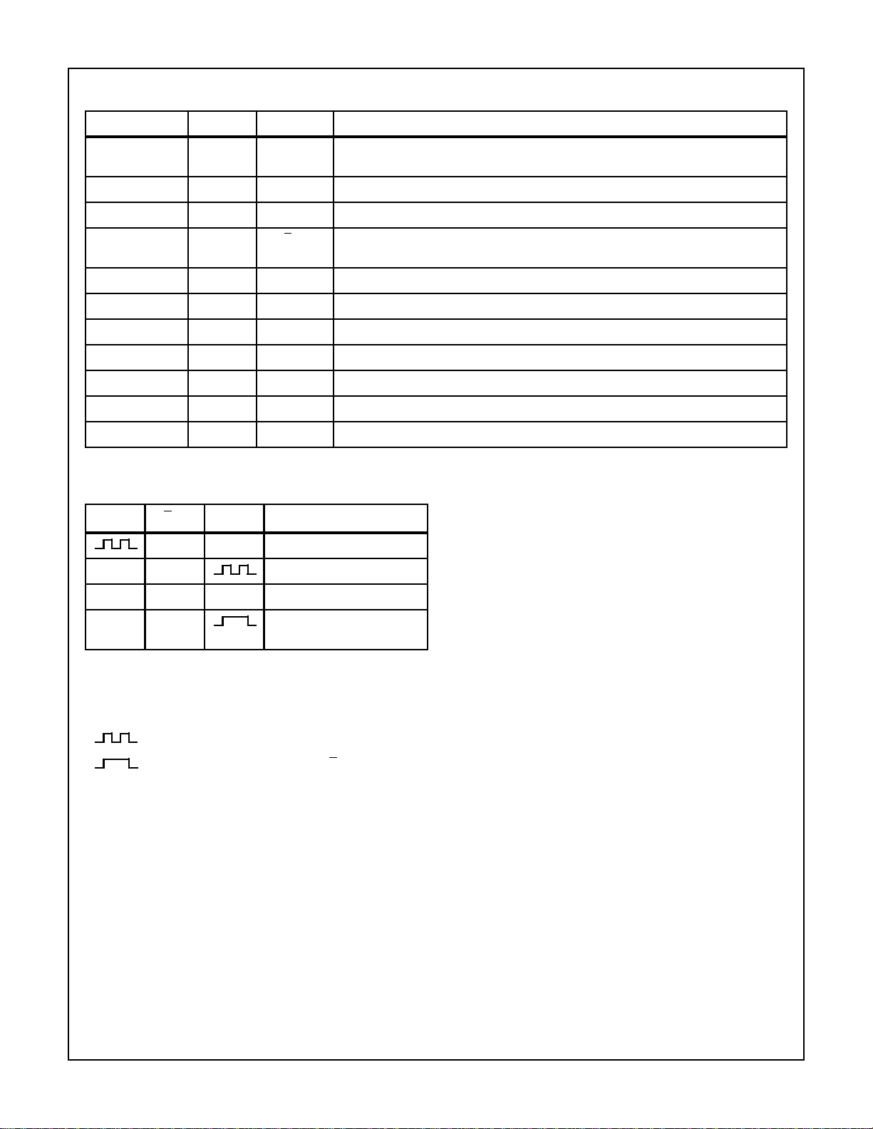
Switching Waveforms
tW(H) tW(L)
CP/I
I
M/SN
CO
X
50%
50%
50%
t
s
t
h
50%
NOTE:
1. Setup and Hold times are shown as positive values but may be specified as negative values.
50%
AC Testing Input, Output Waveform
INPUT
V
IH
V
IL
50%
50%
NOTE:
1. AC Testing: All input signals must switch between VIL and V
Input rise and fall times are driven at 1ns per volt.
IH.
All Intersil semiconductor products are manufactured, assembled and tested under ISO9000 quality systems certification.
Intersil products are sold by description only. Intersil Corporation reserves the right to make changes in circuit design and/or specifications at any time without
notice. Accordingly, the reader is cautioned to verify that data sheets are current before placing orders. Information furnished by Intersil is believed to be accurate
and reliable. However, no responsibility is assumed by Intersil or its subsidiaries for its use; nor for any infringements of patents or other rights of third parties which
may result from its use. No license is granted by implication or otherwise under an y patent or patent rights of Intersil or its subsidiaries.
For information regarding Intersil Corporation and its products, see web site http://www.intersil.com
OUTPUT
V
OH
V
OL
Sales Office Headquarters
NORTH AMERICA
Intersil Corporation
P. O. Box 883, Mail Stop 53-204
Melbourne, FL 32902
TEL: (407) 724-7000
FAX: (407) 724-7240
EUROPE
Intersil SA
Mercure Center
100, Rue de la Fusee
1130 Brussels, Belgium
TEL: (32) 2.724.2111
FAX: (32) 2.724.22.05
ASIA
Intersil (Taiwan) Ltd.
Taiwan Limited
7F-6, No. 101 Fu Hsing North Road
Taipei, Taiwan
Republic of China
TEL: (886) 2 2716 9310
FAX: (886) 2 2715 3029
5-7
 Loading...