

Page 1
HD1750FX
HIGH VOLTAGE NPN POWER TRANSISTOR FOR HIGH
DEFINITION AND NEW SUPER-SLIM CRT DISPLAYS
■ STATE-OF-THE-ART TECHNOLOGY:
DIFFUSED COLLECTOR "ENHANCED
GENERATION" EHVS1
■ WIDER RANGE OF OPTIMUM DRIVE
CONDITIONS
■ LESS SENSITIVE T O OPERATING
TEMPERATURE VARIATION
■ FULLY INSULA TED POWER PACKAGE U .L .
COMPLIANT
APPLICATIONS
■ HORIZONTAL DEFLECTION OUTPUT FOR
DIGITAL TV, HDTV AND HIGH-END
MONITORS
DESCRIPTION
The device is manufactured using Diffused
Collector in Planar technology adopting "Enhance
High Voltage Struc ture" (EHVS1) d eveloped to fit
High-Definition CRT displays.
The new HD product series show improved silicon
efficiency bringing updated performance to the
Horizontal Deflection stage.
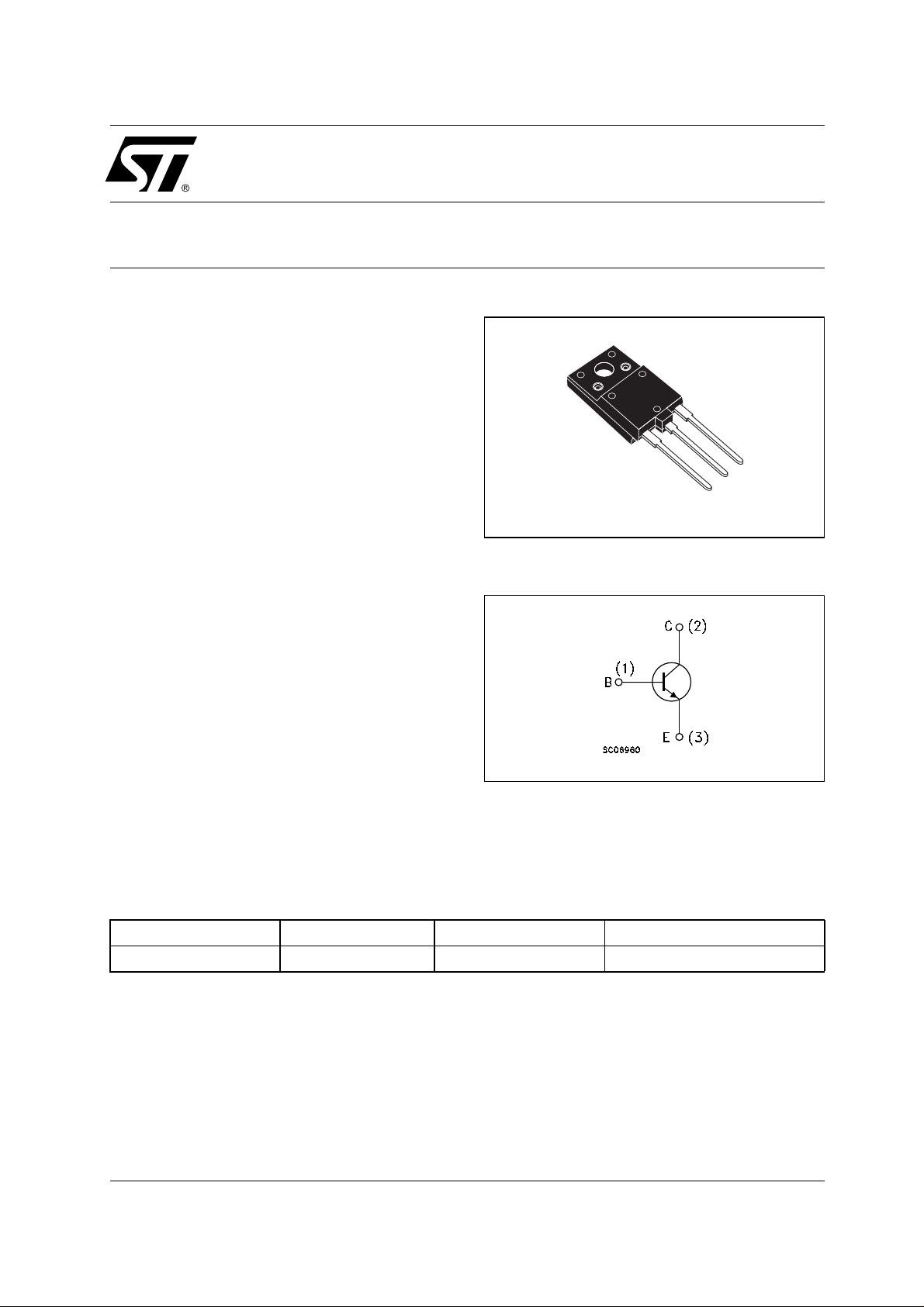
Figure 1: Package
ISOWATT218FX
Figure 2: Internal Schematic Diagram
Table 1: Order Codes
Part Number Marking Package Packaging
HD1750FX HD1750FX ISOWATT218FX TUBE
Rev. 2
1/8December 2005
Page 2
HD1750FX
Table 2: Absolute Maximum Ratings
Symbol Parameter Value Unit
V
CES
V
CEO
V
EBO
I
I
CM
I
I
BM
P
V
T
T
Table 3: Thermal Data
R
thj-case
Collector-Emitter Voltage (VBE = 0)
Collector-Emitter Voltage (IB= 0)
Emitter-Base Voltage (IC= 0)
Collector Current
C
Collector Peak Current (tp < 5ms)
Base Current
B
Base Peak Current (tp < 5ms)
Total Dissipation at TC = 25 oC
tot
Insulation Withstand Voltage (RMS) from All Three Leads to
ins
External Heatsink
Storage Temperature
stg
Max. Operating Junction Temperature
J
Thermal Resistance Junction-Case Max 1.67
1700 V
800 V
10 V
24 A
36 A
12 A
18 A
75 W
2500 V
-65 to 150 °C
150 °C
o
C/W
Table 4: Electrical Characteristics (T
= 25 oC unless otherwise specified)
case
Symbol Parameter Test Conditions Min. Typ. Max. Unit
I
CES
I
EBO
V
CEO(sus)
Collector Cut-off Current
(V
= 0)
BE
Emitter Cut-off Current
(I
= 0)
C
* Collector-Emitter
Sustaining Voltage
= 1700 V
V
CE
= 1700 V TC = 125 oC
V
CE
= 5 V 10 µA
V
EB
IC = 10 mA 800 V
0.2
2
(IB = 0 )
V
V
CE(sat)
V
BE(sat)
h
EBO
Emitter-Base Voltage
(I
= 0 )
C
* Collector-Emitter
Saturation Voltage
* Base-Emitter Saturation
Voltage
DC Current Gain IC = 1 A VCE = 5 V
FE
INDUCTIVE LOAD
t
Storage Time
s
t
Fall Time
f
INDUCTIVE LOAD
t
Storage Time
s
Fall Time
t
f
* Pulsed: P ul sed duratio n = 300 ms, duty cycle ≤ 1.5 %.
= 10 mA 10 V
I
E
IC = 12 A IB = 3 A 3 V
IC = 12 A IB = 3 A 0.95 1.5 V
30
= 12 A VCE = 5 V
I
C
6.5
9.5
IC = 12 A fh = 31250 Hz
= 1.9 A I
I
B(on)
= 1320 V V
V
CE(fly)
= 0.8 µH
L
BB(off)
I
= 6.5 A fh = 100 kHz
C
= 1.2 A I
I
B(on)
= 1220 V V
V
CE(fly)
= 0.25 µH
L
BB(off)
B(off)
BE(off)
B(off)
BE(off)
= -8.1 A
= -5.85 A
= -2.7 V
= -2.7 V
3.1
350
1.7
1802250
3.8
500
mA
mA
µs
ns
µs
ns
2/8
Page 3
HD1750FX
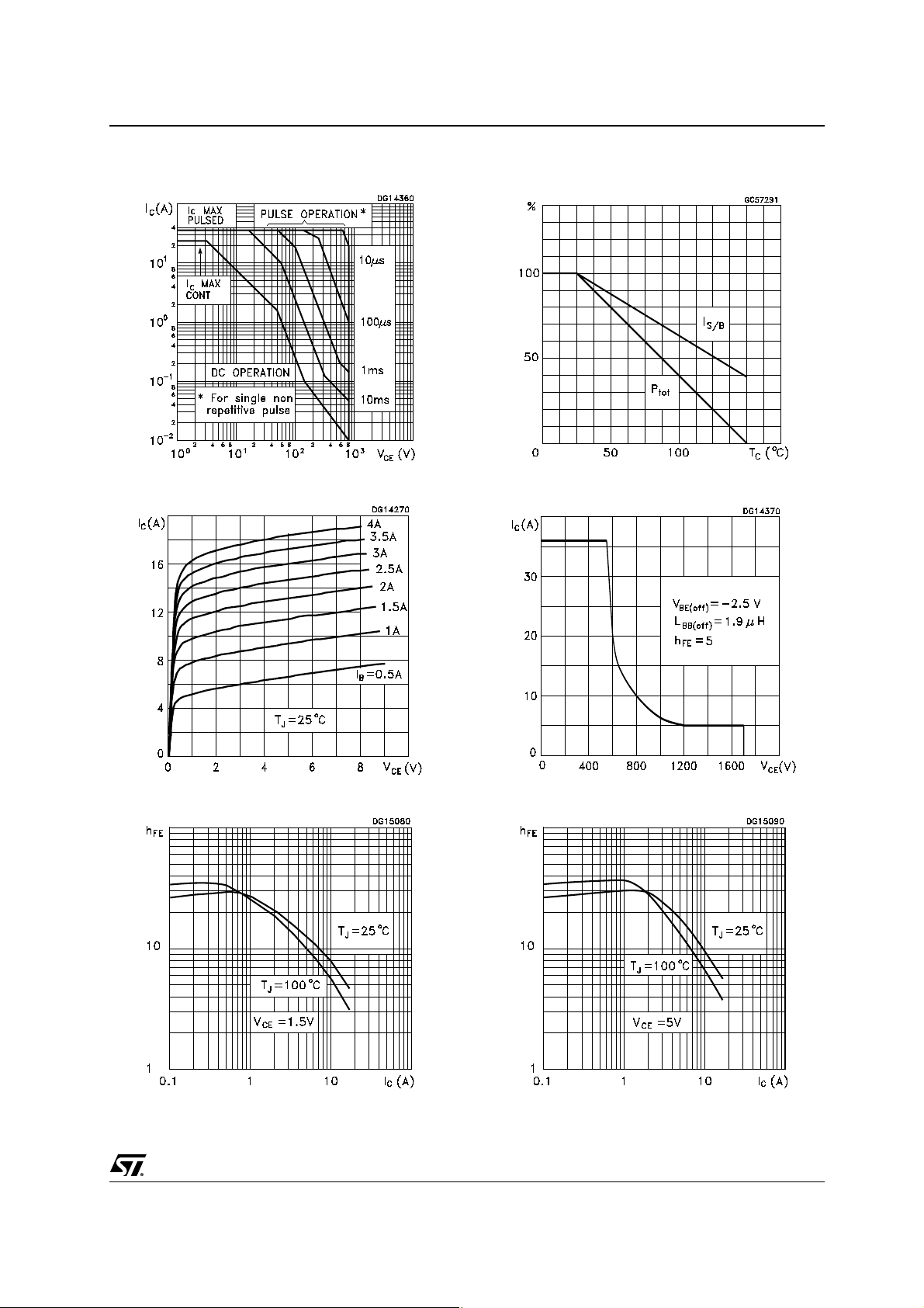
Figure 3: Safe Operating Area
Figure 4: Output Chatacterisctics
Figure 6: Deratin g C urve
Figure 7: Reverse Biased SOA
Figure 5: DC Current Gain
Figure 8: DC Current Gain
3/8
Page 4
HD1750FX
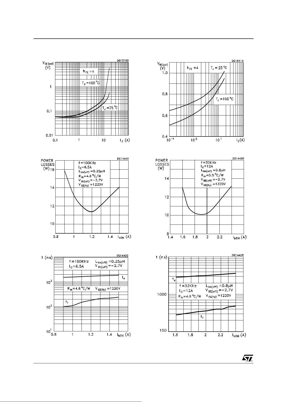
Figure 9: Collector-Emitter Saturation Voltage
Figure 10: Power Los ses
Figure 12: Base-Emitter Saturation Voltage
Figure 13: Power Los ses
Figure 11: Inductive Load Switching Time
4/8
Figure 14: Inductive Load Switching Time
Page 5
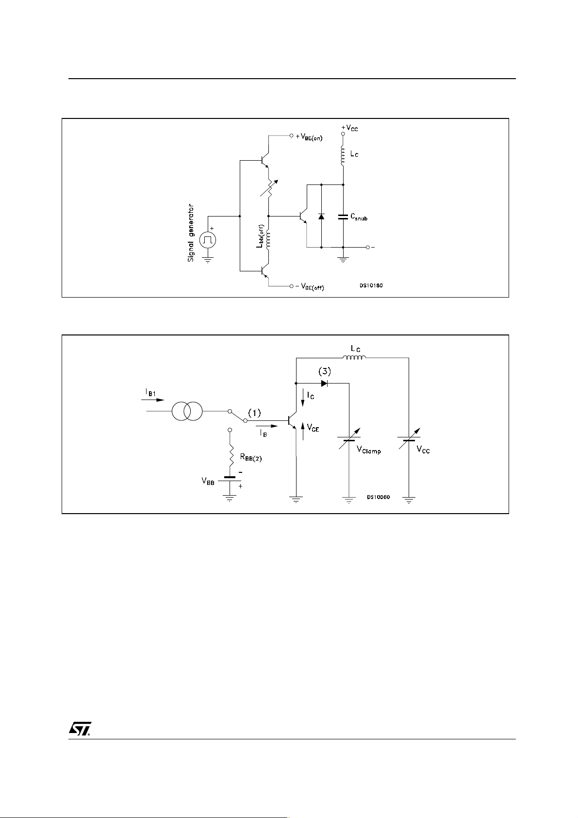
Figure 15: Power Losses and Inductive Load Switching Test Circui t
Figure 16: Reverse Biased Safe Operating Area Test Circuit
HD1750FX
5/8
Page 6
HD1750FX
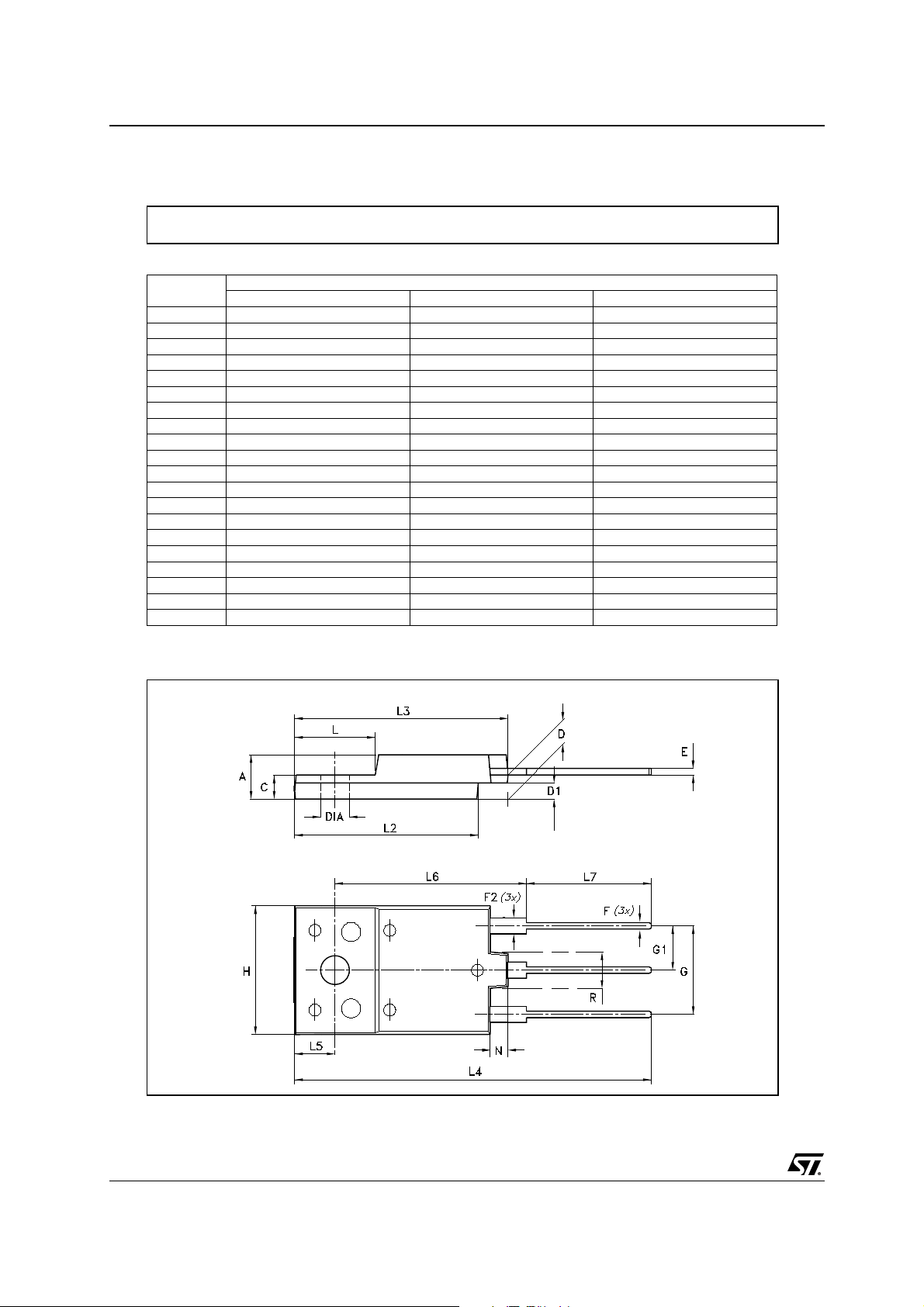
ISOWATT218FX MECHANICAL DATA
DIM.
A 5.30 5.70
C 2.80 3.20
D 3.10 3.50
D1 1.80 2.20
E 0.80 1.10
F 0.65 0.95
F2 1.80 2.20
G 10.30 11.50
G1 5.45
H 15.30 15.70
L9 10.20
L2 22.80 23.20
L3 26.30 26.70
L4 43.20 44.40
L5 4.30 4.70
L6 24.30 24.70
L7 14.60 15
N 1.80 2.20
R 3.80 4.20
Dia 3.40 3.80
MIN. TYP MAX.
mm.
6/8
7627132 B
Page 7
Figure 5: Revision History
Release Date Version Change Designator
30-May-2005 1 Initial Release.
19-Dec-2005 2
New h
value in table 4
FE
HD1750FX
7/8
Page 8

HD1750FX
I
s
o
d
b
t
t
t
a
nformation furnished is believed to be accurate and reliable. However, STMicroelectronics assumes no responsibility for the consequence
f use of such information nor for any infringement of patents or other rights of third parties which may result from its use. No license is grante
y implicat io n or ot h er wis e under an y pat e nt or pa te nt r igh ts of STMi c roe l ec tro ni c s. Sp ec i fi ca ti on s ment i o ne d in th is p ub li c ati on ar e s ub jec
o change without notice. This publication supersedes an d replaces all informat ion previously supplied. STMicroelectronics products are no
uthorized for use as critical components in life support device s or systems without express written approval of STMicroelectronics.
The ST logo is a registered trademark of STMicroelectronics
All other names are the property of their respective owners
© 2005 STMicroelectronics - All Rights Reserved
Australia - Belgium - Brazil - Canada - China - Czech Republic - Finland - France - Germany - Hong Kong - India - Israel - Italy - Japan -
Malaysia - Malta - Morocco - Singapore - Spain - Sweden - Switzerland - United Kingdom - United States of America
STMicroelectronics group of companies
www.st.com
8/8
 Loading...