

HD-15531/883
March 1997
Features
• This Circuit is Processed in Accordance to MIL-STD883 and is Fully Conformant Under the Provisions of
Paragraph 1.2.1.
• Support of MIL-STD-1553
• Data Rate (15531B) . . . . . . . . . . . . . . . 2.5 Megabit/Sec
• Data Rate (15531). . . . . . . . . . . . . . . . 1.25 Megabit/Sec
• Variable Frame Length to 32-Bits
• Sync Identification and Lock-In
• Separate Manchester II Encode, Decode
• Low Operating Power . . . . . . . . . . . . . . . . .50mW at 5V
CMOS Manchester Encoder-Decoder
Description
The Intersil HD-15531/883 is a high performance CMOS
device intended to service the requirements of MIL-STD1553 and similar Manchester II encoded, time division multiplexed serial data protocols. This LSI chip is divided into two
sections, an Encoder and a Decoder. These sections operate independently of each other, except for the master reset
and word length functions. This circuit provides many of the
requirements of MIL-STD-1553. The Encoder produces the
sync pulse and the parity bit as well as the encoding of the
data bits. The Decoder recognizes the sync pulse and identifies it as well as decoding the data bits and checking parity.
The HD-15531/883 also surpasses the requirements of MILSTD-1553 by allowing the word length to be programmable
(from 2 to 28 data bits). A frame consists of three bits for
sync followed b y the data word (2 to 28 data bits) followed by
one bit of parity, thus, the frame length will vary from 6 to 32
bit periods. This chip also allows selection of either even or
odd parity for the Encoder and Decoder separately.
This integrated circuit is fully guaranteed to support the
1MHz data rate of MIL-STD-1553 over both temperature and
voltage. For high speed applications the 15531B will support
a 2.5 Megabit/sec data rate.
The HD-15531/883 can also be used in many party line digital data communications applications, such as a local area
network or an environmental control system driven from a
single twisted pair or fiber optic cable throughout a building.
Ordering Information
PACKAGE TEMPERATURE RANGE 1.25MBIT/SEC 2.5MBIT/SEC PKG. NO.
CERDIP -55oC to +125oC HD1-15531/883 HD1-15531B/883 F40.6
CAUTION: These devices are sensitive to electrostatic discharge; follow proper IC Handling Procedures.
http://www.intersil.com or 407-727-9207
| Copyright © Intersil Corporation 1999
5-170
File Number 2962.1
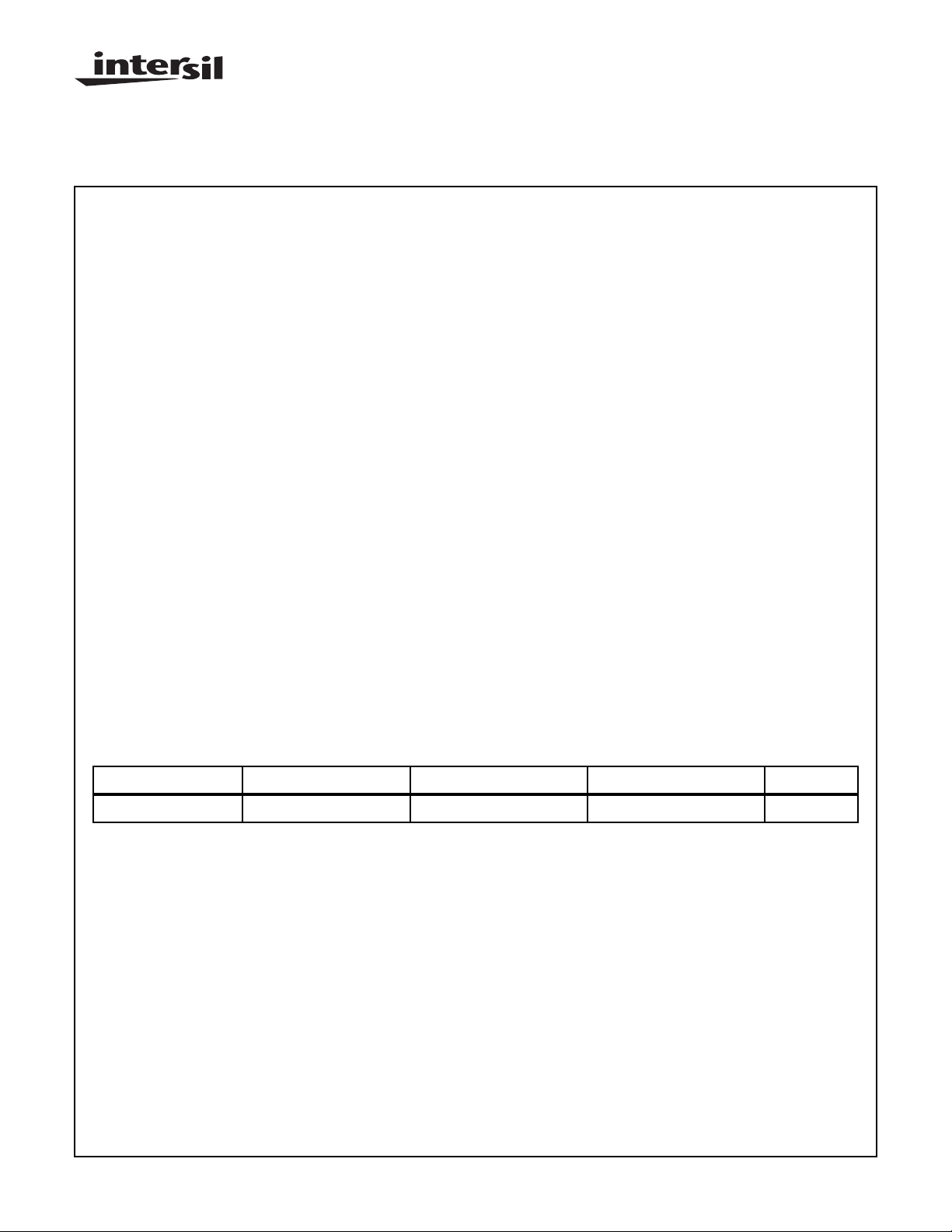
Pinout
VCC
VALID WORD
TAKE DATA’
TAKE DATA
SERIAL DATA OUT
SYNCHR DATA
SYNCHR DATA SEL
SYNCHR CLK
DECODER CLK
SYNCHR CLK SEL
BIPOLAR ZERO IN
BIPOLAR ONE IN
UNIPOLAR DATA IN
DECODER SHIFT CLK
TRANSITION SEL
NC
COMMAND SYNC
DECODER PARITY SEL
DECODER RESET
COUNT C0
HD-15531/883
HD-15531/883 (CERDIP)
TOP VIEW
1
2
3
4
5
6
7
8
9
10
11
12
13
14
15
16
17
18
19
20
40
39
38
37
36
35
34
33
32
31
30
29
28
27
26
25
24
23
22
21
COUNT C1
COUNT C4
DATA SYNC
ENCODER CLK
COUNT C3
NC
ENCODER SHIFT CLK
SEND CLK IN
SEND DATA
ENCODER PARITY SEL
SYNC SEL
ENCODER ENABLE
SERIAL DATA IN
BIPOLAR ONE OUT
OUTPUT INHIBIT
BIPOLAR ZERO OUT
÷ 6 OUT
COUNT 2
MASTER RESET
GND
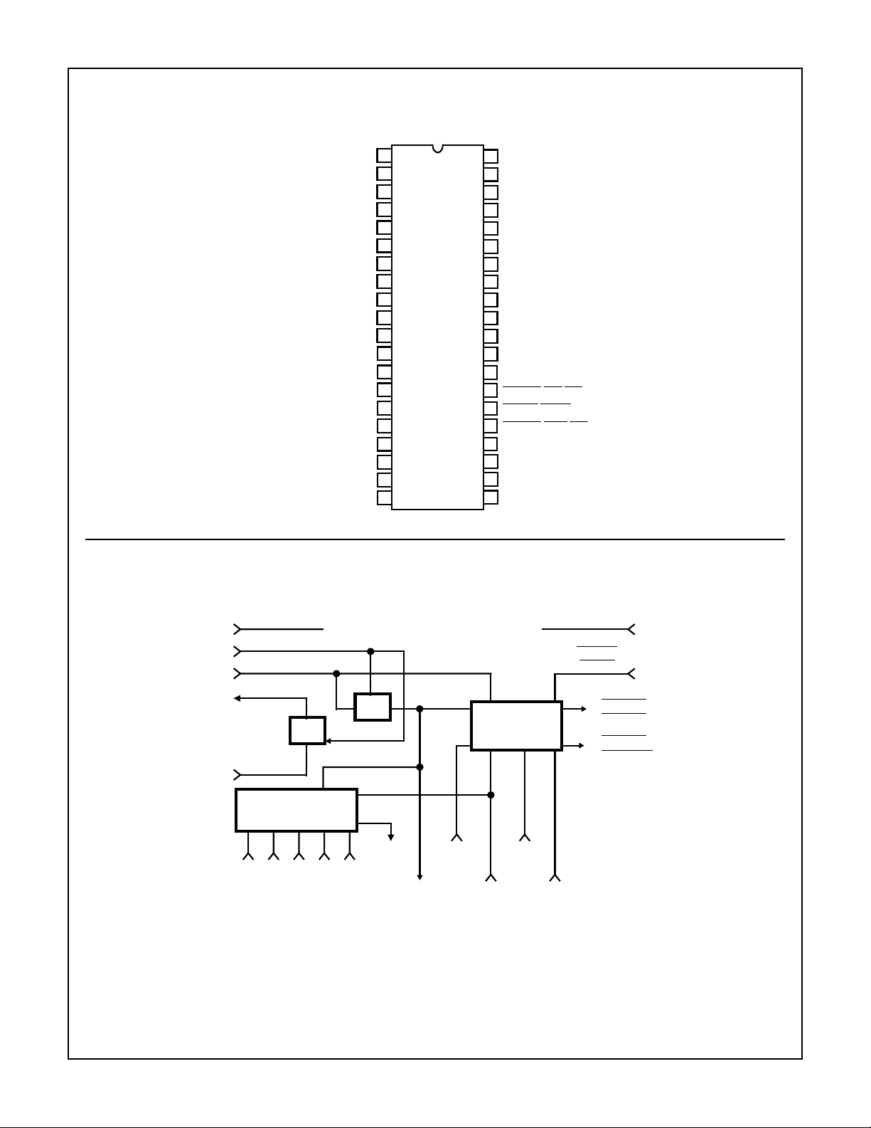
Block Diagrams
GND
21
MASTER RESET
22
SEND CLK IN
33
6 OUT
24
ENCODER
37
CLK
BIT
COUNTER
20 40 23 36 39
C0C1C2C3C
÷ 6
ENCODER
V
CC
1
OUTPUT
INHIBIT
ENCODER
PARITY
SELECT
27
25
÷ 2
CHARACTER
FORMER
34 28 29 31
32
SEND
DAT A
4
ENCODER
SHIFT
CLK
SERIAL
DATA IN
ENCODER
ENABLE
30
SYNC
SELECT
26
BIPOLAR
ONE OUT
BIPOLAR
ZERO OUT
5-171
HD-15531/883
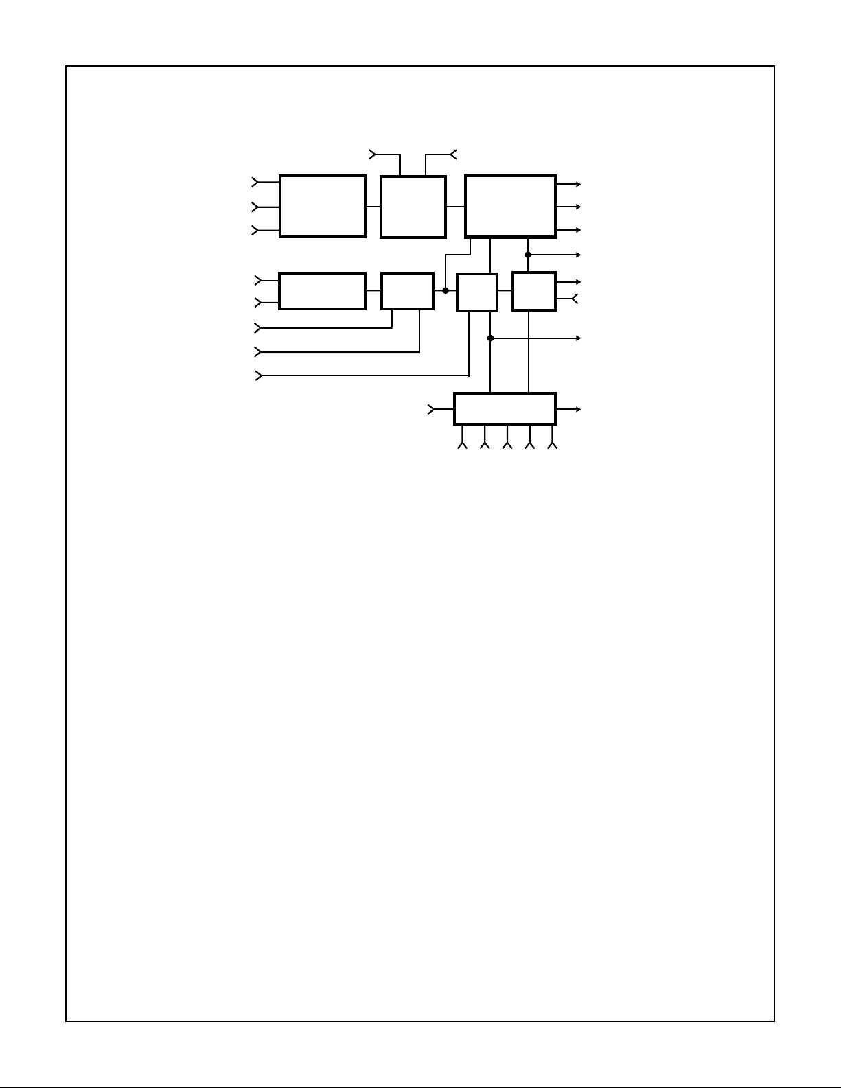
Block Diagrams
CLK SELECT
SYNCHRONOUS
SYNCHRONOUS
CLK SELECT
(Continued)
UNIPOLAR
DATA IN
BIPOLAR
ONE IN
BIPOLAR
ZERO IN
DECODER
CLK
DECODER
CLK
MASTER
RESET
SYNCHRONOUS
DATA SELECT
13
12
TRANSITION
FINDER
11
9
SYNCHRONIZER
15
8
10
22
DECODER
7 8
DAT A
SELECT
GATE
CLOCK
SELECT
DAT A
DECODER
RESET
SYNCHRONOUS
DAT A
CHARACTER
IDENTIFIER
BIT
RATE
CLK
19
20 40 23 36 39
C0 C1 C2 C3 C4
BIT
COUNTER
PARITY
CHECK
4
17
38
5
2
16
14
3
TAKE DATA
COMMAND
DATA SYNC
SERIAL
DATA OUT
VALID WORD
PARITY
SELECT
DECODER
SHIFT CLK
TAKE DATA
5-172

HD-15531/883
Absolute Maximum Ratings Thermal Information
Supply Voltage . . . . . . . . . . . . . . . . . . . . . . . . . . . . . . . . . . . . .+7.0V
Input, Output or I/O Voltage . . . . . . . . . . . GND -0.5V to VCC +0.5V
ESD Classification . . . . . . . . . . . . . . . . . . . . . . . . . . . . . . . . Class 1
CAUTION: Stresses above those listed in “Absolute Maximum Ratings” may cause permanent damage to the device. This is a stress only rating and operation
of the device at these or any other conditions above those indicated in the operational sections of this specification is not implied.
Operating Conditions
Supply Voltage . . . . . . . . . . . . . . . . . . . . . . . . . . . . . +4.5V to +5.5V
Operating Temperature Range (TA) . . . . . . . . . . . . -55oC to +125oC
Encoder/Decoder Clock Rise Time (TECR, TDCR). . . . . . .8ns Max
Encoder/Decoder Clock Fall Time (TECF, TDCF) . . . . . . . .8ns Max
TABLE 1. HD-15531/883, HD-15531B/883 DC ELECTRICAL PERFORMANCE SPECIFICATIONS
P ARAMETER
Input LOW Voltage VIL VCC = 4.5V and 5.5V 1, 2, 3 -55oC ≤ TA ≤ +125oC - 0.2 VCC V
SYMBOL
TEST CONDITIONS
Thermal Resistance θ
CERDIP Package . . . . . . . . . . . . . . . . . . 35oC/W 9oC/W
Maximum Storage Temperature Range . . . . . . . . .-65oC to +150oC
Maximum Junction Temperature. . . . . . . . . . . . . . . . . . . . . .+175oC
Maximum Lead Temperature (Soldering 10s). . . . . . . . . . . .+300oC
JA
θ
Die Characteristics
Gate Count . . . . . . . . . . . . . . . . . . . . . . . . . . . . . . . . . . . .250 Gates
Sync. Transition Span (TD2). . . . . . . . . . . 18 TDC Typical, (Note 1)
Short Data Transition Span (TD4). . . . . . . . 6 TDC Typical, (Note 1)
Long Data Transition Span (TD5) . . . . . . . 12 TDC Typical, (Note 1)
GROUP A
SUBGROUPS TEMPERA TURE
LIMITS
UNITSMIN MAX
JC
Input HIGH Voltage VIH VCC = 4.5V and 5.5V 1, 2, 3 -55oC ≤ TA ≤ +125oC 0.7 VCC - V
Input LOW Clock Voltage VILC VCC = 4.5V and 5.5V 1, 2, 3 -55oC ≤ TA ≤ +125oC - GND +0.5 V
Input HIGH Clock Voltage VIHC VCC = 4.5V and 5.5V 1, 2, 3 -55oC ≤ TA ≤ +125oC VCC -0.5 - V
Output LOW Voltage VOL IOL = +1.8mA,
VCC = 4.5V (Note 2)
Output HIGH Voltage VOH IOH = -3.0mA,
VCC = 4.5V (Note 2)
Input Leakage Current II VI = VCC or GND,
VCC = 5.5V
Standby Supply Current ICCSB VIN = VCC = 5.5V,
Outputs Open
Functional Test FT (Note 3) 7, 8 -55oC ≤ TA ≤ +125oC- - -
NOTES:
1. TDC = Decoder clock period = 1/FDC.
2. Interchanging of force and sense conditions is permitted.
3. Tested as follows: f = 15MHz, VIH = 70% VCC, VIL = 20% VCC, CL = 50pF, VOH ≥ VCC/2 and VOL ≤ VCC/2.
TABLE 2. HD-15531/883, HD-15531B/883 AC ELECTRICAL PERFORMANCE SPECIFICATIONS
GROUP A
P ARAMETER SYMBOL
ENCODER TIMING
Encoder
Clock
Frequency
Send Clock
Frequency
FEC VCC = 4.5V and 5.5V 9, 10, 11 -5 5oC ≤TA≤+125oC - 15 - 30 MHz
FESC VCC = 4.5V and 5.5V 9, 10, 11 -55oC ≤TA≤+125oC - 2.5 - 5.0 MHz
(NOTE 2)
CONDI-TIONS
SUB-
GROUPS TEMPERA TURE
1, 2, 3 -55oC ≤ TA ≤ +125oC - 0.4 V
1, 2, 3 -55oC ≤ TA ≤ +125oC 2.4 - V
1, 2, 3 -55oC ≤ TA ≤ +125oC -1.0 +1.0 µA
1, 2, 3 -55oC ≤ TA ≤ +125oC- 2 mA
HD-15531/883 HD-15531B/883
UNITSMIN MAX MIN MAX
5-173

HD-15531/883
TABLE 2. HD-15531/883, HD-15531B/883 AC ELECTRICAL PERFORMANCE SPECIFICATIONS (Continued)
GROUP A
(NOTE 2)
P ARAMETER SYMBOL
Encoder Data
Rate
Master Reset
Pulse Width
Shift Clock
Delay
Serial Data
Setup
Serial Data
Hold
Enable Setup TE4 VCC = 4.5V and 5.5V 9, 10, 11 -55oC ≤TA≤+125oC90 - 90 - ns
Enable Pulse
Width
Sync Setup TE6 VCC = 4.5V and 5.5V 9, 10, 11 -55oC ≤TA≤+125oC55 - 55 - ns
Sync Pulse
Width
Send Data
Delay
Bipolar Output
Delay
Enable Hold TE10 VCC = 4.5V and 5.5V 9, 10, 11 -55oC ≤TA≤+125oC10 - 10 - ns
Sync Hold TE11 VCC = 4.5V and 5.5V 9, 10, 11 -55oC ≤TA≤+125oC95 - 95 - ns
DECODER TIMING
Decoder
Clock
Frequency
Decoder
Sync Clock
Decoder Data
Rate
Decoder Reset Pulse
Width
Decoder Reset Setup
Time
Decoder Reset Hold Time
Master Reset
Pulse
Bipolar Data
Pulse Width
One Zero
Overlap
Sync Delay
(ON)
FED VCC = 4.5V and 5.5V 9, 10, 11 -55oC ≤TA≤+125oC - 1.25 - 2.5 MHz
TMR VCC = 4.5V and 5.5V 9, 10, 11 -55oC ≤TA≤+125oC 150 - 150 - ns
TE1 VCC = 4.5V and 5.5V 9, 10, 11 -55oC ≤TA≤+125oC - 125 - 80 ns
TE2 VCC = 4.5V and 5.5V 9, 10, 11 -55oC ≤TA≤+125oC75 - 50 - ns
TE3 VCC = 4.5V and 5.5V 9, 10, 11 -55oC ≤TA≤+125oC75 - 50 - ns
TE5 VCC = 4.5V and 5.5V 9, 10, 11 -55oC ≤TA≤+125oC 100 - 100 - ns
TE7 VCC = 4.5V and 5.5V 9, 10, 11 -55oC ≤TA≤+125oC 150 - 150 - ns
TE8 VCC = 4.5V and 5.5V 9, 10, 11 -55oC ≤TA≤+125oC0 50 0 50ns
TE9 VCC = 4.5V and 5.5V 9, 10, 11 -55oC ≤TA≤+125oC - 130 - 130 ns
FDC VCC = 4.5V and 5.5V 9, 10, 11 -55oC ≤TA≤+125oC - 15 - 30 MHz
FDS VCC = 4.5V and 5.5V 9, 10, 11 -55oC ≤TA≤+125oC - 2.5 - 5.0 MHz
FDD VCC = 4.5V and 5.5V 9, 10, 11 -55oC ≤TA≤+125oC - 1.25 - 2.5 MHz
TDR VCC = 4.5V and 5.5V 9, 10, 11 -55oC ≤TA≤+125oC 150 - 150 - ns
TDRS VCC = 4.5V and 5.5V 9, 10, 11 -55oC ≤TA≤+125oC75 - 75 - ns
TDRH VCC = 4.5V and 5.5V 9, 10, 11 -55oC ≤TA≤+125oC10 - 10 - ns
TMR VCC = 4.5V and 5.5V 9, 10, 11 -55oC ≤TA≤+125oC 150 - 150 - ns
TD1 VCC = 4.5V and 5.5V 9, 10, 11 -55oC ≤TA≤+125oC TDC +10
TD3 VCC = 4.5V and 5.5V 9, 10, 11 -55oC ≤TA≤+125oC - TDC-10
TD6 VCC = 4.5V and 5.5V 9, 10, 11 -55oC ≤TA≤+125oC -20 110 -20 110 ns
CONDI-TIONS
SUB-
GROUPS TEMPERA TURE
HD-15531/883 HD-15531B/883
- TDC +10
(Note 1)
(Note 1)
(Note 1)
- TDC-10
UNITSMIN MAX MIN MAX
-ns
ns
(Note 1)
5-174

HD-15531/883
TABLE 2. HD-15531/883, HD-15531B/883 AC ELECTRICAL PERFORMANCE SPECIFICATIONS (Continued)
GROUP A
(NOTE 2)
P ARAMETER SYMBOL
Take Data
Delay (ON)
Serial Data
Out Delay
Sync Delay
(OFF)
Take Data
Delay (OFF)
Valid Word
Delay
Sync Clock to
Shift Clock
Delay
Sync Data
Setup
NOTES:
1. TDC = Decoder Clock Period = 1/FDC.
2. AC Testing as follows: VIH = 70% VCC, VIL = 20% VCC; Input rise/fall times driven at 1ns/V; Timing reference levels: VCC/2;
Output load: CL = 50pF.
TD7 VCC = 4.5V and 5.5V 9, 10, 11 -55oC ≤TA≤+125oC 0 110 0 110 ns
TD8 VCC = 4.5V and 5.5V 9, 10, 11 -55oC ≤TA≤+125oC- 80 - 80ns
TD9 VCC = 4.5V and 5.5V 9, 10, 11 -55oC ≤TA≤+125oC 0 110 0 110 ns
TD10 VCC = 4.5V and 5.5V 9, 10, 11 -55oC ≤TA≤+125oC 0 110 0 110 ns
TD11 VCC = 4.5V and 5.5V 9, 10, 11 -55oC ≤TA≤+125oC 0 110 0 110 ns
TD12 VCC = 4.5V and 5.5V 9, 10, 11 -55oC ≤TA≤+125oC- 75 - 75ns
TD13 VCC = 4.5V and 5.5V 9, 10, 11 -55oC ≤TA≤+125oC75 - 75 - ns
CONDI-TIONS
SUB-
GROUPS TEMPERA TURE
HD-15531/883 HD-15531B/883
UNITSMIN MAX MIN MAX
TABLE 3. HD-15531/883, HD-15531B/883 ELECTRICAL PERFORMANCE SPECIFICATIONS
LIMITS
PARAMETER SYMBOL CONDITIONS NOTES TEMPERATURE
Input Capacitance CI VCC = OPEN, f = 1MHz, All measure-
ments referenced to device GND
Input/Output Capacitance
Operating Power
Supply Current
NOTES:
1. The parameters listed in Table 3 are controlled via design or process parameters are characterized upon initial design and after major
process and/or design changes.
2. Guaranteed but not 100% tested.
CONFORMANCE GROUPS METHOD SUBGROUPS
Initial Test 100%/5004 Interim Test 100%/5004 1, 7, 9
PDA 100%/5004 1
Final Test 100%/5004 2, 3, 8A, 8B, 10, 11
CIO VCC = OPEN, f = 1MHz, All measure-
ments referenced to device GND
ICCOP VCC = 5.5V, f = 1MHz 1, 2 -55oC ≤ TA ≤ +125oC - 10 mA
TABLE 4. APPLICABLE SUBGROUPS
1T
1T
= +25oC - 25 pF
A
= +25oC - 25 pF
A
UNITSMIN MAX
Group A Samples/5005 1, 2, 3, 7, 8A, 8B, 9, 10, 11
Groups C & D Samples/5005 1, 7, 9
5-175

Burn-In Circuit
HD-15531/883
HD1-15531/883 CERDIP
VCC
V
CC
GND
VCC
FO
GND
GND
VCC
NC
GND
GND
VCC
1
A
A
A
A
A
A
R
R
R
R
R
R
R
R
R
R
2
3
4
5
6
7
8
9
10
11
12
13
14
15
16
17
18
19
20
R
40
39
38
37
36
35
34
33
32
31
30
29
28
27
26
25
24
23
22
21
R
R
R
R
R
R
R
R
R
R
R
VCC
VCC
A
FO
GND
NC
A
A
VCC
GND
VCC
GND
VCC
A
VCC
GND
GND
NOTES:
1. VCC = 5.5V ±0.5V.
2. VIH = 4.5V ±10%.
3. VIL = -0.2V to +0.4V.
4. R = 47kΩ±5%.
5. F0 = 100kHz ±10%.
VCC
GND
R
R
A
R
5-176

Die Characteristics
HD-15531/883
DIE DIMENSIONS:
155 x 195 x 19 ±1mils
METALLIZATION:
Type: Si-Al
Thickness: 11k
Å ±2kÅ
Metallization Mask Layout
TAKE DATA
SERIAL DATA OUT
SYNCHR DATA
SYNCHR DATA SEL
GLASSIVATION:
Type: SiO
2
Thickness: 8kű1kÅ
WORST CASE CURRENT DENSITY:
5
2.0 x 10
HD-15531/883
VALID WORD
TAKE DATA’ COUNT C4VCC ENCODER CLK
COUNT C1
A/cm
2
DATA SYNC
COUNT C3
ENCODER SHIFT CLK
SEND CLK IN
SYNCHR CLK
DECODER CLK
SYNCHR CLK SEL
BIPOLAR ZERO IN
BIPOLAR ONE IN
UNIPOLAR DATA IN
DECODER SHIFT CLK
TRANSITION SEL
COMMAND SYNC
DECODER
PARITY SEL
DECODER GND
RESET
SEND DATA
ENCODER PARITY SEL
SYNC SEL
ENCODER ENABLE
SERIAL DATA IN
BIPOLAR ONE OUT
OUTPUT INHIBIT
BIPOLAR ZERO OUT
COUNTMASTERCOUNT
RESETC0
2
÷6 OUT
All Intersil semiconductor products are manufactured, assembled and tested under ISO9000 quality systems certification.
Intersil products are sold by description only. Intersil Corporation reserves the right to make changes in circuit design and/or specifications at any time without
notice. Accordingly, the reader is cautioned to verify that data sheets are current before placing orders. Information furnished by Intersil is believed to be accurate
and reliable. However, no responsibility is assumed by Intersil or its subsidiaries for its use; nor for any infringements of patents or other rights of third parties which
may result from its use. No license is granted by implication or otherwise under an y patent or patent rights of Intersil or its subsidiaries.
For information regarding Intersil Corporation and its products, see web site http://www.intersil.com
5-177
 Loading...