

Page 1

HD155121F
RF Transceiver IC for GSM and PCN Dual band cellular systems
ADE-207-265A (Z)
2nd Edition
May 1999
Description
The HD155121F is a RF transceiver IC for GSM and PCN dual band cellular systems, and integrates most
of the low power silicon functions of a transceiver. The HD155121F incorporates two bias circuits for RF
LNAs, two first mixers, a second mixer, a programmable gain amplifier, and an IQ demodulator for the
receiver, and an IQ modulator and offset PLL for the transmitter. Also, on chip are dividers for the phase
splitter. Moreover the HD155121F includes control circuits to implement power saving modes. These
functions can operate down to 2.7 V and are housed in a 48-pin LQFP SMD package.
Hence the HD155121F can form a small size transceiver handset for dual band by adding a dual PLL
frequency synthesizer IC, power amplifiers and some external components.
The HD155121F is fabricated using a 0.6 µm double-polysilicon Bi-CMOS process.
Functions
Receiver(Rx)
• Low Noise Amplifier (LNA) bias circuit
• First mixer
• IF amplifier and second mixer
• Programmable Gain Amplifier (PGA)
• IQ demodulator with 90 degree phase splitter
Transmitter(Tx)
• IQ modulator with 90 degree phase splitter
• Offset PLL
Down converter
Phase comparator
TXVCO driver
Others
• IF dividers
• Power saving control circuit
• IFVCO
Page 2

HD155121F
Features
• Highly integrated RF processing for hand-portables
• Operating supply voltage
VCC : 2.7 to 3.6 V
Phase comparator and TXVCO driver circuit : 2.7 to 5.25 V
• Current consumption
Rx mode (GSM) : 53 mA + LNA current
Rx mode (PCN) : 52 mA + LNA current
Tx mode (GSM) : 36 mA
Tx mode (PCN) : 37 mA
Idle mode :1 µA
• Operating temperature : –20 to +75 degree
• LQFP 48pin SMD (Low Profile Quad Flat Package)
• Wide operating frequencies
Rx RF GSM : 925 - 960 MHz
PCN : 1805 - 1880 MHz
1st IF : 225 MHz
2nd IF : 45 MHz
Tx RF GSM : 880 - 915 MHz
PCN : 1710 - 1785 MHz
IF GSM : 270 MHz
PCN : 135 MHz
• Offset PLL architecture for Transmitter
• High dynamic range Programmable Gain Amplifier (PGA)
2
Page 3
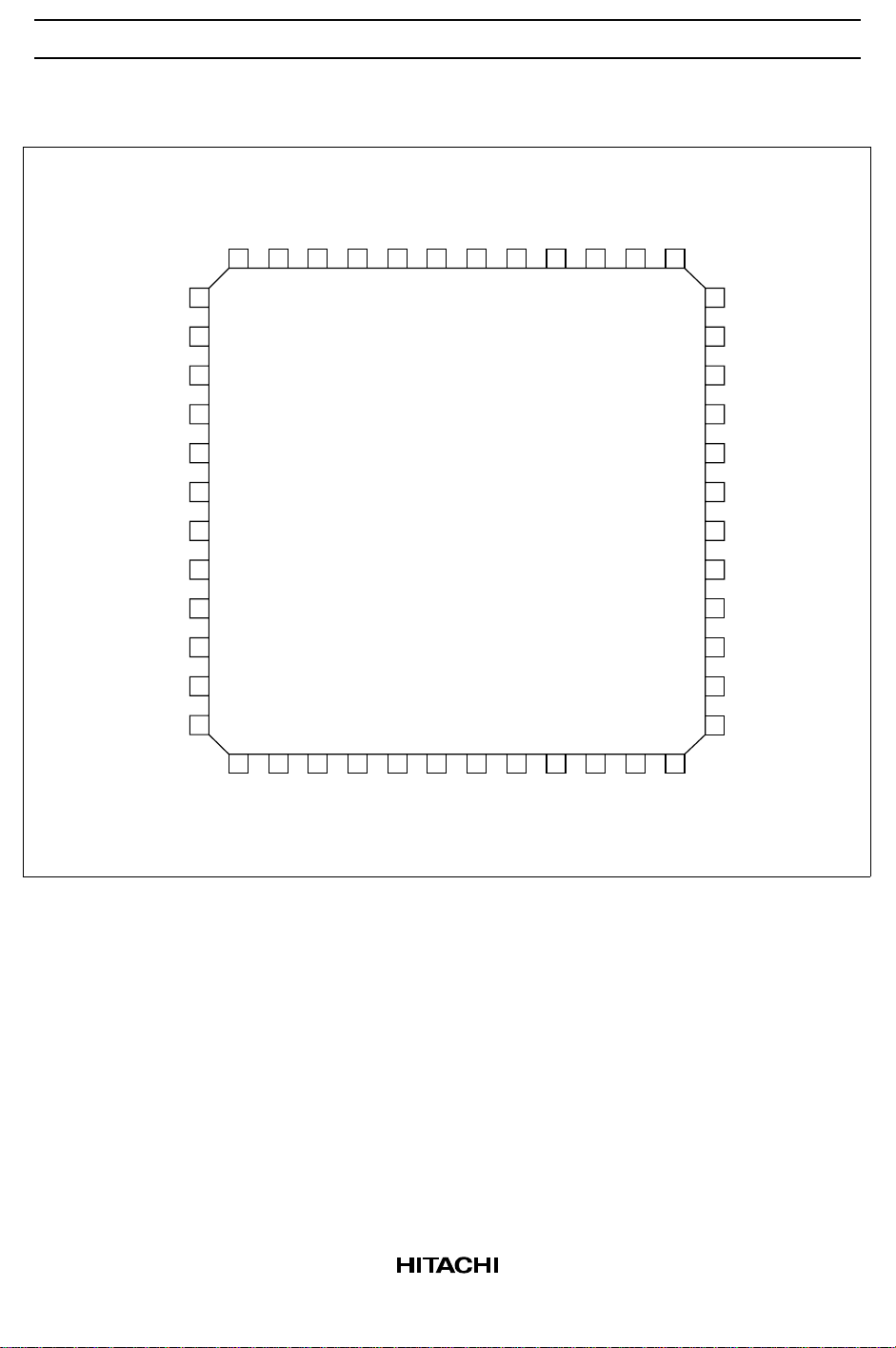
Pin Arrangement
MIX1INB1
1
MIX1IN2
MIX1INB2
POONTX
POONRX2
POONRX1
MIX1OUTB
MIX1OUT
VCCMIX1
GNDMIX1
RFLOIN
VCCDIV
GNDDIV
373839404142434445464748
36
HD155121F
IFLO
MIX1IN1
RFOUT
RFIN1
RFIN2
VCCPLL
GNDPLL
VCOIN2
VCOIN1
VCCCOMP
PLLOUT
ICURAD
2
3
4
5
6
7
8
9
10
11
12
1413 24232221201918171615
QINB
QIN
IINB
IIN
VCCIQ
MODLB
(Top View)
GNDIQ
QOUTB
QOUT
IOUTB
IOUT
35
34
33
32
31
30
29
28
27
26
25
MIX2OB
BAND
IFVCOO
IFVCOI
VCCIF
GNDIF
IFIN
IFINB
LE
SDATA
CLK
MIX2O
3
Page 4

HD155121F
Pin Description
Pin No. Pin Name Description
1 MIX1INB1 Negative input for Mixer1 (GSM)
2 MIX1IN1 Positive input for Mixer1 (GSM)
3 RFOUT Bias for the collector of LNA transistor
4 RFIN1 Bias for the base of LNA transistor (GSM)
5 RFIN2 Bias for the base of LNA transistor (PCN)
6 VCCPLL VCC for OPLL
7 GNDPLL GND for OPLL
8 VCOIN2 TxVCO signal input (PCN)
9 VCOIN1 TxVCO signal input (GSM)
10 VCCCOMP VCC for phase comparator
11 PLLOUT Current output to control and modulate the TxVCO
12 ICURAD Phase comparator output current setting
13 QINB Negative input of Q signal for modulator
14 QIN Positive input of Q signal for modulator
15 IINB Negative input of I signal for modulator
16 IIN Positive input of I signal for modulator
17 MODLB VCC for modulator load bias
18 VCCIQ VCC for IQ modulator and demodulator
19 GNDIQ GND for IQ modulator and demodulator
20 QOUTB Negative output of Q signal for modulator
21 QOUT Positive output of Q signal for modulator
22 IOUTB Negative output of I signal for modulator
23 IOUT Positive output of I signal for modulator
24 MIX2OB Negative output for Mixer2
25 MIX2O Positive output for Mixer2
26 CLK Clock for serial data
27 SDATA Serial data for Gain control
28 LE Load enable for serial data
29 IFINB Negative input for Mixer2
30 IFIN Positive input for Mixer2
31 GNDIF GND for Mixer2 and PGA
32 VCCIF VCC for Mixer2 and PGA
33 IFVCOI Base of IFVCO transistor
34 IFVCOO Emitter of IFVCO transistor
4
Page 5

Pin Description (cont)
Pin No. Pin Name Description
35 BAND Band control (Low: GSM, High: PCN)
36 IFLO Output of IFVCO or Input of IF Local
37 GNDDIV GND for Divider and IFVCO
38 VCCDIV VCC for Divider and IFVCO
39 RFLOIN Input for RF Local
40 GNDMIX1 GND for Mixer1
41 VCCMIX1 VCC for Mixer1
42 MIX1OUT Positive output for Mixer1 (GSM/PCN)
43 MIX1OUTB Negative output for Mixer1 (GSM/PCN)
44 POONRX1 Power save control for LNA and Mixer1
45 POONRX2 Power save control for Mixer2, PGA and demodulator
46 POONTX Power save control for modulator and OPLL
47 MIX1INB2 Negative input for Mixer1 (PCN)
48 MIX1IN2 Positive input for Mixer1 (PCN)
HD155121F
5
Page 6
HD155121F
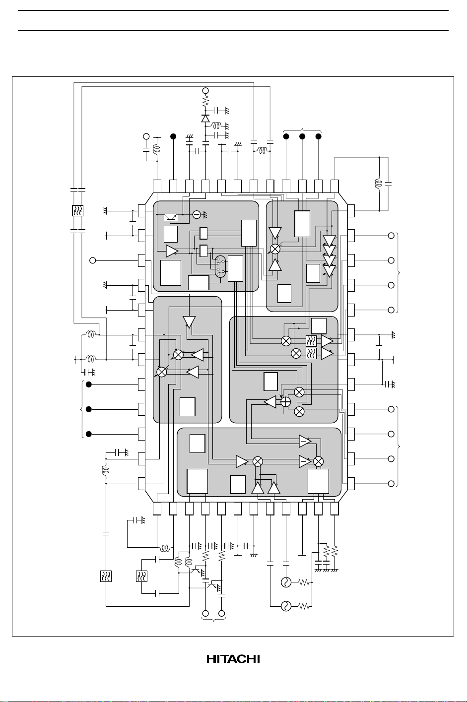
Block Diagram
Tune
GNDDIV
VCCDIV
1172MHz
(Rx: 1580MHz, Tx: 1575MHz)
from VCO
GNDMIX1
VCCMIX1
MIX1OUT
MIX1OUTB
POONRX1
POONRX2
RFLOIN
225MHz
(225MHz)
from
System controller
IFLO
BAND
IFVCOO
36
35
540
MHz
Vref
(IFVCO)
Vref
(Div.Rx)
(Div.Tx)
Vref
34
from
(Mix1)
IFVCOI
33
1/2 1/6
Band
SW
VCCIF
GNDIF
32
1/2
(1580/1575MHz) 1172MHz
GSM: 270MHz
225MHz
(225MHz)
IFIN
IFINB
31
30
1/2
(90deg)
(90deg)
45MHz
270MHz
(135MHz)
PCN: 135MHz
from System controller
LE
SDATA
CLK
29
28
27
26
Serial
interface
Vref
(PGA)
(IF)
Vref
(45MHz)
Vref
(Mod)
45MHz
(45MHz)
Vref
MIX2O
25
(Demod)
MIX2OB
23
IOUT
IOUTB
QOUT
QOUTB
GNDIQ
VCCIQ
MODB
IIN
45MHz
to Base bandfrom Base band
driver
ICURAD
IINB
QIN
13 14 15 16 17 18 19 20 21 22 24
12
RICURAD
from System controller
POONTX
MIX1INB2
MIX1IN2 QINB
(1805MHz)
47 46 45 44 43 42 41 40 39 38 37
48
947MHz
1
2
MIX1IN1
MIX1INB1
Vref
(LNA)
LNA
Bias
circuit
3
4
RFIN1
RFOUT
947MHz
from Antenna
1172MHz
(1580/
1575MHz)
Vref
5
RFIN2
VCCPLL
(1805MHz)
(PLL)
6
7
VCOIN2
GNDPLL
(1710MHz)
8
270MHz
(135MHz)
9
VCOIN1
902MHz
Tx.VCO1Tx.VCO2
mode
Current
10
11
PLLOUT
VCCCOMP
6
Page 7
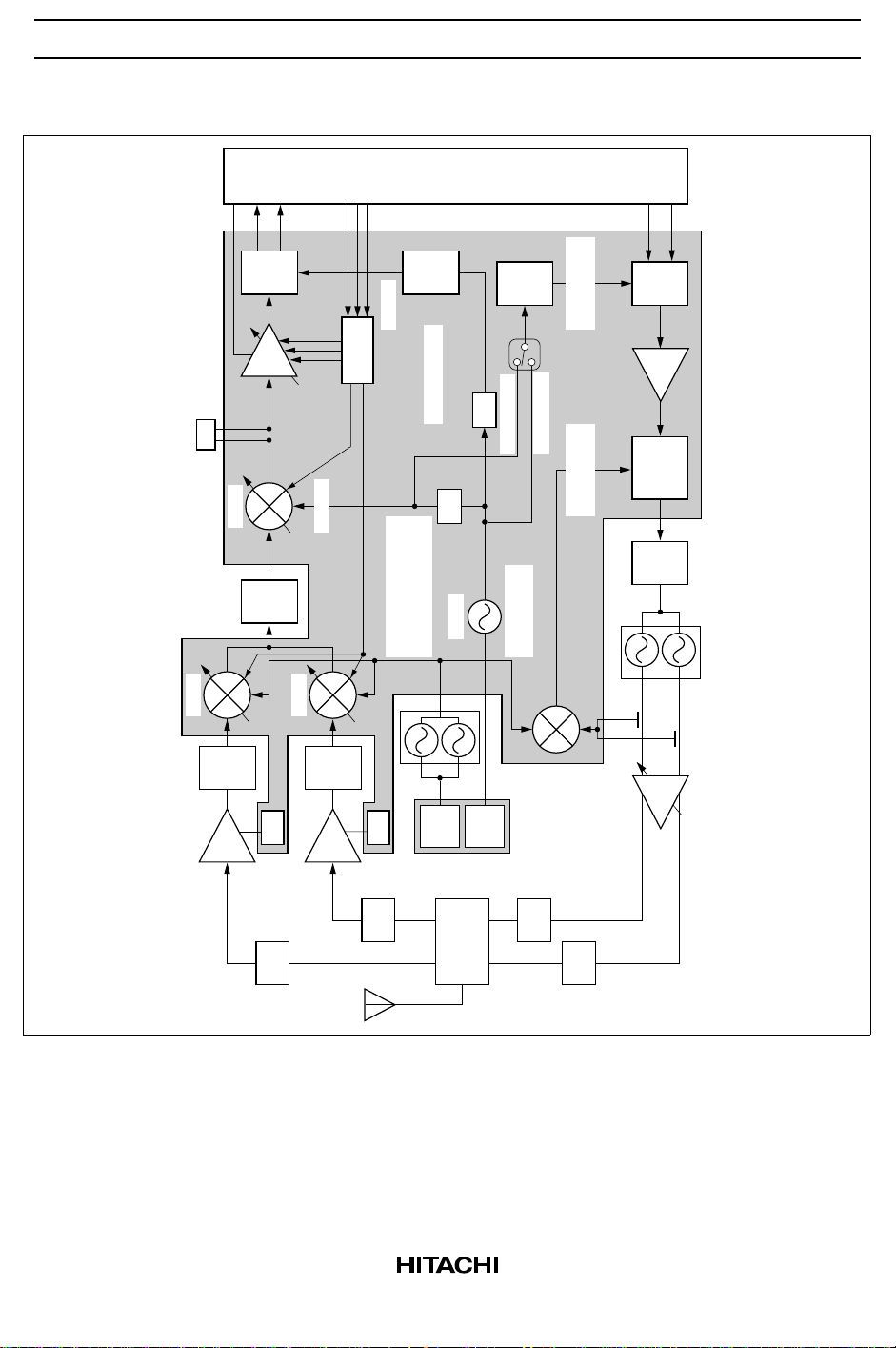
Configuration
HD155121F
B.B.
I
Q
Block
I
Q
LC
45 MHz
Mixer2
225 MHz
Mixer1
RF
SAW
LNA
925 to 960 MHz
filter
IF
I & Q
PGA
SAW
bias
RF
Demo.
filter
Mixer1
circuit
filter
270 MHz
RF
SAW
LNA
1805 to
1880 MHz
45 MHz
interface
Serial data
: 1150 to 1185 MHz
GSM
filter
bias
circuit
RF
filter
÷2
Shift
90 deg
HD155121F
÷2
: Rx. 1580 to 1655 MHz
/Tx. 1575 to 1650 MHz
PCN
RF VCO
PLL1
Dual
synth.
90 deg
÷6
PCN: 270 MHz
IFVCO
GSM: 540 MHz
PLL2
HD155017T
S/W
÷2
Shift
GSM: 270 MHz
PCN: 135 MHz
GSM: 540 MHz
GSM: 270 MHz
PCN: 135 MHz
PCN: 540 MHz
LPF
LPF
Mod
I & Q
Phase
Detector
filter
Loop
880 to 915 MHz
880 to 915 MHz
1710 to 1785 MHz
1710 to 1785 MHz
PA Module
7
Page 8

HD155121F
Functional Operation
The HD155121F has been designed from system stand point and incorporated a large number of the circuit
blocks necessary in the design of a digital cellular handset.
Receiver Operation
The HD155121F incorporates two LNA bias circuits for external RF transistors, whose NF and power gain
can be better selected.
This circuit amplifies the RF signal after selection by the antenna filter before the signal enters the first
mixer section. The RF signal is combined with a local oscillator (LO) signal to generate a wanted first IF
signal in the 130 - 300 MHz range. The first mixer circuit uses a double-balanced Gilbert cell architecture,
which has open collector differential outputs. If, at 225 MHz, a 800 Ω LC load is connected to the mixer’s
outputs then a SSB NF of 9.0 dB (GSM), 9.1 dB (PCN) with a gain of 9.5 dB (GSM), 8.5 dB (PCN) is
realizable. The corresponding input compression point is –10.5 dBm (GSM), –12.5 dBm (PCN), which
allows the device to be used within a GSM and EGSM and PCN system.
A filter is used after the first mixer to provide image rejection and the conditioned signal is then passed
through an intermediate amplifier, before being down converted to a second IF in the range of 26 - 60
MHz.
The second mixer can generate a 45 MHz second IF, if a 270 MHz second local signal is used. The second
mixer also uses the Gilbert cell architecture, but with internal resistive differential outputs of 300 Ω. If
amplifier and second mixer has a SSB NF of 6.0 dB, a power gain of 13 dB and a input compression point
of –22 dBm. In order to improve the blocking characteristics of the device an external LC resonator across
the differential outputs of the second mixer is recommended.
First mixer and second mixer can switch the power gain. Switching gain step of first mixer is 12 dB, and
such step of second mixer is 16 dB.
The signal is then passed to the PGA circuit, which has a dynamic range of more than 80 dB (–42 dB - +56
dB typ.) and is controlled by digital serial data, which is generated by the microprocessor. This gain step is
2 dB.
The signal is then down converted by a demodulator to I and Q. Internal divider circuits convert the IFLO
signal to the same frequency as the second IF before passing this local signal through a phase splitter /
shifter in order to generate the in phase and quadrature phase IQ components. The phase accuracy of the
IQ demodulator is less than +/–1 degree and the amplitude mismatch is less than +/–0.5 dB. In order to
accommodate different baseband interfaces the HD155121F IQ differential outputs have a voltage swing of
1.6 Vpp and DC offset of less than +/–60 mV. Within each output stage a second order Butterworth filter
(fc = 210 kHz) is used to improve the blocking performance of the device.
In order to allow flexibility in circuit implementation the HD155121F can configured to use either a singleended or balanced external circuitry and components.
8
Page 9

HD155121F
Transmitter Operation
The transmitter chain converts differential IQ baseband signals to a suitable format for transmission by a
power amplifier.
The common mode voltage range of the modulator inputs is 0.8 V to 1.2 V and they have 2.0 Vpp
differential swing. The modulator circuit uses double-balanced mixers for the I and Q paths. The Local
signals are generated by dividing the IFLO signals by 2, and then passed to the modulator through a phase
splitter / shifter. The IF signals generated are then summed to produce a single modulated IF signal which
is amplified and fed into the offset PLL block. Carrier suppression due to the mixer circuit is better than 31
dBc. If the common mode DC voltage of the I and Q inputs is adjusted, carrier suppression is better than
40 dBc easily. Side band suppression is better than 35 dBc without adjustment.
Within the offset PLL block there are a down converter, a phase comparator and a VCO driver. The down
converter mixes the first local signal and the TXVCO signal to create a reference local signal for use in the
offset PLL circuit. The phase comparator and the VCO driver generate an error current, which is
proportional to the phase differential between the reference IF and the modulated IF signals. This current is
used in a second order loop filter to generate a voltage, which in turn modulates the TXVCO. In order to
optimize the PLL loop gain, the error current value can be modified by changing the value of an external
resistor - ICURAD. In order to accommodate various control range of TXVCOs, the offset PLL circuit has
been designed to operate with a supply voltage up to 5.25 V.
9
Page 10

HD155121F
Operation Modes
The HD155121F has necessary control circuitry to implement the necessary states within the dual band
system. Also provided is a power saving mode which reduces the current consumption of the device by
powering down unnecessary function blocks. Three pins are assigned for power saving mode control,
POONRX1, POONRX2 and POONTX. Also one pin is assigned for switching operational band, BAND.
Table 1 shows the relationship between the pins and the required operating mode. These pins are
controlled by the system controller.
As per GSM requirements the Tx and Rx sections do not operate simultaneously. For the receiver there is a
calibration mode in which the LNA bias circuit and first mixer are switched off. During this period the
gain of the PGA can be adjusted. Also the DC offsets of the IQ demodulator are measured and
subsequently canceled.
In order to change between the Rx and Tx modes a state called “warm-up” is used to ensure that the local
signals are not unduly affected. This method of switching between Tx and Rx ensures that lock is achieved
first time.
Power saving is implemented through use of the idle mode. All function blocks of the HD155121F are
switched off until such time as the system controller commands the device to power up again.
Table 1 Operating Modes with Power Saving
Mode Receive Calibrate Warm-up Transmit Idle
Band GSM PCN — — GSM PCN —
POONRX1 (44) H H L L L L H
POONRX2 (45) H H H L L L L
POONTX (46) L L L L H H Don’t care
BAND (35) L H Don’t care Don’t care L H Don’t care
Rx block LNA bias (GSM) ON OFF OFF OFF OFF OFF OFF
LNA bias (PCN) OFF ON OFF OFF OFF OFF OFF
1st Mixer (GSM) ON OFF OFF OFF OFF OFF OFF
1st Mixer (PCN) OFF ON OFF OFF OFF OFF OFF
2nd Mixer ON ON ON OFF OFF OFF OFF
PGA ON ON ON OFF OFF OFF OFF
I/Q demodulator ON ON ON OFF OFF OFF OFF
Tx block Offset PLL OFF OFF OFF OFF ON ON OFF
I/Q modulator OFF OFF OFF OFF ON ON OFF
Oscillator IF VCO ON ON ON ON ON ON OFF
block Divider (Rx) ON ON ON OFF OFF OFF OFF
Divider (Tx) OFF OFF OFF OFF ON ON OFF
1st local buffer ON ON ON ON ON ON OFF
IF local buffer ON ON ON ON ON ON OFF
Total current 53 mA 52 mA 34 mA 9.0 mA 36 mA 37 mA 1 µA
10
Page 11

HD155121F
Absolute Maximum Ratings
Any stress in excess of the absolute maximum ratings can cause permanent damage to the HD155121F.
Item Symbol Rating Unit
Power supply voltage (V
Power supply voltage (V
Pin voltage V
Maximum power dissipation P
Operating temperature Topr –20 to +75 °C
Storage temperature Tstg –55 to +125 °C
)VCC–0.3 to +4.0 V
CC
)V
CCCOMP
CCCOMP
T
T
–0.3 to +5.5 V
–0.3 to VCC+0.3 (4.0 Max) V
400 mW
11
Page 12

HD155121F
CCCO
Electrical Characteristics
DC Specifications (VCC = 3 V, Ta = 25°C unless otherwise specified.)
Item Mode Min Typ Max Unit Test Condition Note
Power supply voltage (VCC) 2.7 3.0 3.6 V
Power supply voltage (V
Power supply current (Rx.) GSM — 53.0 74.0 mA VCC = 3.0V, V
Power supply current (Tx.) GSM — 36.0 50.0 mA VCC = 3.0V, V
Power supply current (Warm-up) — 9.0 12.5 mA VCC = 3.0V, V
Power saving mode supply current — 1.0 10.0 µAVCC = 3.0V, V
Power up time (Rx.) — 1.5 5.0 µsec from PS mode 1
Power up time (Tx.) — 0.2 0.5 µsec from PS mode 1
Power on control voltage range
(POONRX1, POONRX2, POONTX)
Power off control voltage range
(POONRX1, POONRX2, POONTX)
I/Q common-mode output voltage 1.15 1.35 1.55 V
I/Q maximum output swing
(Single ended)
I/Q output DC offset voltage –60 0 60 mV VIOUTDC – VIOUTBDC,
I/Q common-mode input voltage 0.8 1.0 1.2 V 1
I/Q input swing (Single ended) 0.8 1.0 1.2 Vp-p VIIN, VIINB, VQIN, VQINB 1
Serial data VH (CLK, SDATA, LE) 2.3 — — V
Serial data VL (CLK, SDATA, LE) — — 0.8 V
Band control VH (BAND) 2.3 — — V
Band control VL (BAND) — — 0.8 V
Input current
(POONRX1, POONRX2, POONTX,
BAND, CLK, SDATA, LE)
Note: 1. These values are not tested in mass production.
2. Power supply current does not include the LNA bias current.
) 2.7 3.0 5.25 V
CCCOMP
PCN — 52.0 73.0 mA Mixer1, 2 = Gain1,
PCN — 37.0 52.0 mA
2.3 — — V
— — 0.8 V
0.8 1.06 — Vp-p VIOUT, VIOUTB,
–10 0 10 µA
= 3.0V, 2
CCCOMP
PGA = bitNo26
= 3.0V 2
CCCOMP
= 3.0V 2
CCCOMP
= 3.0V
MP
High level = VCC, Low level = 0V
at mode control pin and serial
data pin (POONRX1, RX2, TX,
BAND, CLK (no clock signal),
SDATA, LE)
VQOUT, VQOUTB
VQOUTDC, VQOUTBDC
2
12
Page 13

HD155121F
AC Specifications (VCC = 3 V, Ta = 25°C unless otherwise specified.)
• LNA Bias circuit specifications
Item Mode Min Typ Max Unit Test Condition Note
LNA transistor bias current GSM 4.7 5.6 — mA
PCN 4.7 5.6 — mA
Frequency GSM 925 — 960 MHz 1
PCN 1805 1880 MHz
Power gain GSM — 19.4 — dB RF = 940 MHz 1
PCN — 13.4 — dB RF = 1842 MHz
Noise figure GSM — 1.6 — dB RF = 940 MHz 1
PCN — 1.6 — dB RF = 1842 MHz
3rd order input intercept point GSM — –6.0 — dBm 1
PCN — –2.0 — dBm
3rd order output intercept point GSM — 13 — dBm 1
PCN — 11 — dBm
1dB input compression point GSM — –14.5 — dBm 1
PCN — –9.5 — dBm
1dB output compression point GSM — 3.9 — dBm 1
PCN — 2.9 — dBm
Output (RF) Z GSM — 50 — Ω Output (GSM RF) 1
PCN — 50 — Ω Output (PCN RF)
Input (RF) Z GSM — 50 — Ω Input (GSM RF) 1
PCN — 50 — Ω Input (PCN RF)
Note: 1. These AC characteristics are shown for reference only and do not form part of the HD155121F
component specification.
13
Page 14

HD155121F
• Mixer1 specifications (Differential output load between pin42 and pin43 = 800 Ω)
Item Mode Min Typ Max Unit Test Condition Note
Frequency (RF) GSM 925 — 960 MHz 1
PCN 1805 — 1880 MHz
Frequency (LO) GSM 1125 — 1260 MHz 1
PCN 1505 — 1680 MHz
Frequency (IF) — 200 225 300 MHz 1
RFLO input level — –8.0 — — dBm
Conversion gain 1 GSM 6.5 9.5 12.5 dB RF = 940MHz, LO = 1165MHz, IF = 225MHz 2
PCN 5.5 8.5 11.5 dB RF = 1842MHz, LO = 1617MHz, IF = 225MHz
Conversion gain 2 GSM –5.5 –2.5 0.5 dB RF = 940MHz, LO = 1165MHz, IF = 225MHz 2
PCN –6.5 –3.5 –0.5 dB RF = 1842MHz, LO = 1617MHz, IF = 225MHz
Noise figure 1 GSM — 9.0 10.5 dB RF = 940MHz, LO = 1165MHz, IF = 225MHz 1, 2
PCN — 9.1 10.6 dB RF = 1842MHz, LO = 1617MHz, IF = 225MHz
Noise figure 2 GSM — 15.0 16.5 dB RF = 940MHz, LO = 1165MHz, IF = 225MHz 1, 2
PCN — 16.0 17.5 dB RF = 1842MHz, LO = 1617MHz, IF = 225MHz
3rd order input
intercept point 1
3rd order input
intercept point 2
3rd order output
intercept point 1
3rd order output
intercept point 2
1dB input GSM –12.5 –10.5 — dBm RF = 940MHz, LO = 1165MHz, IF = 225MHz 2
compression point 1 PCN –14.5 –12.5 — dBm RF = 1842MHz, LO = 1617MHz, IF = 225MHz
1dB input GSM –8.5 –6.5 — dBm RF = 940MHz, LO = 1165MHz, IF = 225MHz 2
compression point 2 PCN –10.5 –8.5 — dBm RF = 1842MHz, LO = 1617MHz, IF = 225MHz
1dB output GSM –4.0 –2.0 — dBm RF = 940MHz, LO = 1165MHz, IF = 225MHz 1, 2
compression point 1 PCN –7.0 –5.0 — dBm RF = 1842MHz, LO = 1617MHz, IF = 225MHz
1dB output GSM –12.0 –10.0 — dBm RF = 940MHz, LO = 1165MHz, IF = 225MHz 1, 2
compression point 2 PCN –15.0 –13.0 — dBm RF = 1842MHz, LO = 1617MHz, IF = 225MHz
Note: 1. These values are not tested in mass production.
2. The loss (2.2 dB) of test circuit at Mixer1 output is calculated.
GSM –3.0 –1.0 — dBm RF1 = 940.8MHz, RF2 = 941.6MHz,
LO = 1165MHz, IF = 225MHz
PCN –6.0 –4.0 — dBm RF1 = 1842.8MHz, RF2 = 1843.6MHz,
LO = 1617MHz, IF = 225MHz
GSM 1.0 3.0 — dBm RF1 = 940.8MHz, RF2 = 941.6MHz,
LO = 1165MHz, IF = 225MHz
PCN –3.0 –1.0 — dBm RF1 = 1842.8MHz, RF2 = 1843.6MHz,
LO = 1617MHz, IF = 225MHz
GSM 6.5 8.5 — dBm RF1 = 940.8MHz, RF2 = 941.6MHz,
LO = 1165MHz, IF = 225MHz
PCN 2.5 4.5 — dBm RF1 = 1842.8MHz, RF2 = 1843.6MHz,
LO = 1617MHz, IF = 225MHz
GSM –1.5 0.5 — dBm RF1 = 940.8MHz, RF2 = 941.6MHz,
LO = 1165MHz, IF = 225MHz
PCN –6.5 –4.5 — dBm RF1 = 1842.8MHz, RF2 = 1843.6MHz,
LO = 1617MHz, IF = 225MHz
1, 2
1, 2
1, 2
1, 2
14
Page 15

HD155121F
• Mixer2 specifications
Item Mode Min Typ Max Unit Test Condition Note
Frequency (IF1) 200 225 300 MHz 1
Frequency (LO2) 240 270 360 MHz LO2 = IFLO/2 1
Frequency (IF2) 40 45 60 MHz 1
IFLO input level –10 — — dBm
Conversion gain 1 10.5 13.0 15.5 dB IF1 = 225MHz, IFLO = 540MHz, IF2 = 45MHz 2
Conversion gain 2 –5.5 –3.0 –0.5 dB IF1 = 225MHz, IFLO = 540MHz, IF2 = 45MHz 2
Noise figure 1 — 6.0 7.5 dB IF1 = 225MHz, IFLO = 540MHz, IF2 = 45MHz 1, 2
Noise figure 2 — 12.0 13.5 dB IF1 = 225MHz, IFLO = 540MHz, IF2 = 45MHz 1, 2
3rd order input
intercept point 1
3rd order input
intercept point 2
3rd order output
intercept point 1
3rd order output
intercept point 2
1dB input
compression point 1
1dB input
compression point 2
1dB output
compression point 1
1dB output
compression point 2
Isolation 50 — — dB between Mixer1 output and Mixer2 input 1, 2
Note: 1. These values are not tested in mass production.
2. The loss (3.6 dB) of test circuit at Mixer2 output is calculated.
–15.0 –13.0 — dBm IF1 = 225.8MHz, IF2 = 226.6MHz,
LO = 540MHz, 2ndIF = 45MHz
–11.0 –9.0 — dBm IF1 = 225.8MHz, IF2 = 226.6MHz,
LO = 540MHz, 2ndIF = 45MHz
–2.0 0.0 — dBm IF1 = 225.8MHz, IF2 = 226.6MHz,
LO = 540MHz, 2ndIF = 45MHz
–14.0 –12.0 — dBm IF1 = 225.8MHz, IF2 = 226.6MHz,
LO = 540MHz, 2ndIF = 45MHz
–24.0 –22.0 — dBm IF1 = 225MHz, IFLO = 540MHz, IF2 = 45MHz 2
–21.0 –19.0 — dBm IF1 = 225MHz, IFLO = 540MHz, IF2 = 45MHz 2
–12.0 –10.0 — dBm IF1 = 225MHz, IFLO = 540MHz, IF2 = 45MHz 1, 2
–24.0 –22.0 — dBm IF1 = 225MHz, IFLO = 540MHz, IF2 = 45MHz 1, 2
1, 2
1, 2
1, 2
1, 2
15
Page 16

HD155121F
• PGA and IQ Demodulator specifications (terminated by 10 kΩ at IQ demodulator output)
Item Mode Min Typ Max Unit Test Condition Note
Input frequency 40 45 60 MHz 1
Gain range — 98 — dB 1
Gain linearity –0.8 — 0.8 dB (in any 20dB window) 1
Gain step — 2 — dB 1
Noise figure 1 — 10.9 14 dB IF2 = 45MHz, bitNo46 1, 2
Noise figure 2 — 21.2 24 dB IF2 = 45MHz, bitNo26 1, 2
Noise figure 3 — 53.4 60 dB IF2 = 45MHz, bitNo6 1, 2
Gain 1 47.0 51.5 56.0 dB IF2 = 45MHz, bitNo46 2
Gain 2 7.0 11.5 16.0 dB IF2 = 45MHz, bitNo26 2
Gain 3 –33.0 –28.5 –24.0 dB IF2 = 45MHz, bitNo6 2
i/p CP 1 –70.5 –66 — dBm IF2 = 45MHz, bitNo46 2
i/p CP 2 –37 –34 — dBm IF2 = 45MHz, bitNo26 2
i/p CP 3 –14 –11 — dBm IF2 = 45MHz, bitNo6 2
IQ phase accuracy — 0.2 1.0 deg. Baseband = 67.7kHz
IQ amplitude mismatch — 0.1 0.5 dB Baseband = 67.7kHz 2
Output DC offset voltage 0 — | 60 | mV | IOUT–IOUTB | and
| QOUT–QOUTB |
Load out = 10kΩ
IQ maximum output swing
(Single ended)
I/Q common mode
output voltage
Note: 1. These values are not tested in mass production.
2. The loss (3.6 dB) of test circuit at PGA input is calculated.
0.8 1.06 — Vp-p Baseband = 67.7kHz
IOUT, IOUTB,
QOUT, QOUTB
Load out = 10kΩ
1.15 1.35 1.55 V
16
Page 17

HD155121F
• IQ Modulator and Offset PLL specifications (IFLO is supplied by signal generator equipment)
Item Mode Min Typ Max Unit Test Condition Note
Frequency (RF) GSM 880 — 915 MHz 1
PCN 1710 — 1785 MHz
Frequency (LO) GSM 1150 — 1185 MHz 1
PCN 1530 — 1665 MHz
Frequency (IF) GSM — 270 — MHz
PCN — 135 — MHz
RFLO input level –8 — — dBm
IFLO input level –20 –10 — dBm
VCOIN1 & VCOIN2 input level –25 –15 –10 dBm 1
Carrier suppression ratio 31 40 — dBc All ‘1’ GMSK (Differential encode: off)
(Baseband = 67.7kHz)
Side-band suppression ratio 35 40 — dBc I/Q input swing = 1.0Vp-p,
I/Q common mode
input voltage = 1.0Vdc
Phase accuracy GSM — 1.0 2.5 RMS 200kHz BW 1
GSM — 3.0 7.5 peak 200kHz BW
PCN — 1.0 2.4 RMS 200kHz BW
PCN — 3.0 7.0 peak 200kHz BW
Modulation spectrum GSM — –34.0 — dB 200kHz offset 1
PCN — –34.5 — dB 30kHz bandwidth
Spectrum analyzer condition GSM — –68.0 — dB 400kHz offset 1
Detector mode: positive peak PCN — –67.0 — dB 30kHz bandwidth
GSM — –71.0 — dB 600kHz to 1.8MHz offset 1
PCN — –70.0 — dB 30kHz bandwidth
GSM — –71.5 — dB 1.8MHz to 3MHz offset 1
PCN — –72.0 — dB 100kHz bandwidth
GSM — –74.0 — dB 3MHz to 6MHz offset 1
PCN — –74.0 — dB 100kHz bandwidth
GSM — –76.0 — dB 6MHz upward offset 1
PCN — –76.0 — dB 100kHz bandwidth
Isolation of the 1st local input to
TxVCO input
IQ input swing (Single ended) 0.8 1.0 1.2 Vp-p IIN, IINB, QIN, QINB 1
I/Q common mode input voltage 0.8 1.0 1.2 V IIN, IINB, QIN, QINB 1
PLLOUT output current ratio — 1:0.5 — IPLLOUT GSM : IPLLOUT PCN 1
Phase detector
offset current ratio
Note: 1. These values are not tested in mass production.
— 43 — dB 1
0.30 0.35 0.45 offset current / output current
IIN = 1.5V (DC), IINB = 0.5V (DC)
QIN = 1.5V (DC), QINB = 0.5V (DC)
1
17
Page 18

HD155121F
• IQ Modulator and Offset PLL specifications (IFLO is supplied by signal generator equipment) (cont)
Item Mode Min Typ Max Unit Test Condition Note
Tx noise
in Rx band
Lock up time GSM — 35 80 µsec 1
Note: 1. These values are not tested in mass production.
• IFVCO specifications
Item Mode Min Typ Max Unit Test Condition
Bias current 0.9 2.0 2.5 mA
GSM — –155.1 — dBc/Hz 925MHz to 935MHz
- 10MHz up from Txband
GSM — –164.1 — dBc/Hz 935MHz to 960MHz
- 20MHz up from Txband
PCN — –156 — dBc/Hz 1805MHz - 20MHz up from Txband
PCN — –162 — dBc/Hz 1850MHz - 65MHz up from Txband
PCN — 65 80 µsec
1
18
Page 19

HD155121F
Rx Gain Control Stage
The PGA amplifier of the HD155121F is the main Rx gain control stage. However, Mixer1 and Mixer2
gain level can switched as an optional function in order to optimize system performance.
Mixer1
LNA
LNA
bias
circuit
bias
circuit
Mixer1
Bit allocation
Mixer2
X6 X5 X4 X3 X2 X1 X0
X7
Serial data
X7 : for Mixer1 gain
X6 : for Mixer2 gain
X5 :
X4 :
X3 :
for PGA gain
X2 :
X1 :
X0 :
PGA
Decoder
I&Q
Demo.
Figure 1
Table 2 First Mixer Gain Control Table (as optional function)
Item Band Gain (typ) X7
Gain 1 (normal gain) GSM 9.5 dB 0
PCN 8.5 dB 0
Gain 2 (low gain) GSM –2.5 dB 1
PCN –3.5 dB 1
I
Q
CLK (26)
SDATA (27)
LE (28)
Table 3 Second Mixer Gain Control Table (as optional function)
Item Gain (Typ) X6
Gain 1 (normal gain) 13.0 dB 0
Gain 2 (low gain) –3.0 dB 1
19
Page 20

HD155121F
Table 4 PGA and IQ Demodulator Block Gain Control
bitNo
49
48
47
46
45
44
43
42
41
40
39
38
37
36
35
34
33
32
31
30
29
28
27
26
25
24
23
22
21
20
19
18
17
16
15
14
13
12
11
10
9
8
7
6
5
4
3
2
1
0
Gain (dB)
(Typ)
57.5
55.5
53.5
51.5
49.5
47.5
45.5
43.5
41.5
39.5
37.5
35.5
33.5
31.5
29.5
27.5
25.5
23.5
21.5
19.5
17.5
15.5
13.5
11.5
9.5
7.5
5.5
3.5
1.5
−0.5
−2.5
−4.5
−6.5
−8.5
−10.5
−12.5
−14.5
−16.5
−18.5
−20.5
−22.5
−24.5
−26.5
−28.5
−30.5
−32.5
−34.5
−36.5
−38.5
−40.5
X5
Bit Allocation
X4
1
1
1
1
1
1
1
1
1
1
1
1
1
1
1
1
1
1
0
0
0
0
0
0
0
0
0
0
0
0
0
0
0
0
0
0
0
0
0
0
0
0
0
0
0
0
0
0
0
0
1
1
0
0
0
0
0
0
0
0
0
0
0
0
0
0
0
0
1
1
1
1
1
1
1
1
1
1
1
1
1
1
1
1
0
0
0
0
0
0
0
0
0
0
0
0
0
0
0
0
X3
X2
0
0
1
1
1
1
1
1
1
1
0
0
0
0
0
0
0
0
1
1
1
1
1
1
1
1
0
0
0
0
0
0
0
0
1
1
1
1
1
1
1
1
0
0
0
0
0
0
0
0
0
0
1
1
1
1
0
0
0
0
1
1
1
1
0
0
0
0
1
1
1
1
0
0
0
0
1
1
1
1
0
0
0
0
1
1
1
1
0
0
0
0
1
1
1
1
0
0
0
0
X1
X0
0
0
1
1
0
0
1
1
0
0
1
1
0
0
1
1
0
0
1
1
0
0
1
1
0
0
1
1
0
0
1
1
0
0
1
1
0
0
1
1
0
0
1
1
0
0
1
1
0
0
1
0
1
0
1
0
1
0
1
0
1
0
1
0
1
0
1
0
1
0
1
0
1
0
1
0
1
0
1
0
1
0
1
0
1
0
1
0
1
0
1
0
1
0
1
0
1
0
1
0
20
Page 21

Serial Data Interface
HD155121F
tcyc
CLK
thldtstup
X6 X5 X4 X3 X2 X1 X0X7SDATA
LE
tsule
LSBMSB
twle
Figure 2 Three-Wire Bus Timing Diagram
Serial Data Interface Specifications (VCC = 3 V, Ta = 25°C unless otherwise specified)
Item Symbol Min Typ Max Unit Test Condition Note
Cycle time tcyc 50 — — nsec 1
Setup time tstup 10 — — nsec 1
Hold time thld 10 — — nsec 1
LE setup time tsule 25 — — nsec 1
LE width twle 25 — — nsec 1
Note: 1. These values are not tested in mass production.
2. User can program the data for the PGA, while in any state.
21
Page 22

HD155121F
Test Circuit
1000p
0
VHS LO
IN/OUT(J11)
4p
15n
no fit
0
no fit
VTUNE
no fit
no fitno fitno fit
no fit
BAND
VCC
1000p
MIX2 IF
0
INPUT(J5)
IOUT
IOUTB
QOUT
UHF LO
INPUT(J10)
VCC
VCC
MIX1 IF
OUTPUT(J6)
POONRX1POONTX
POONRX2
RFIN(J7)
DCS MIX1
1000p
1000p
1000p
TOKO
617PT-1206
5
4
3p
12n
no fit
8p
8p
100n
1000p
10k
10k
10k
33p
33p 1p
1000p 1000p
100
68
100
560p
10
10k
1000p
MURATA
MQE9P7-897
6800p
33
390
321
OUT VCC
GND GND
456
Kv=30MHz/V
MIX2 OUTPUT
/PGA INPUT(J1)
IOUT
IOUTB
QOUT
QOUTB
VCC
IIN
IINB
QIN
QINB
MOD CON
TX VCO1
47
3635343332313029282726
IFLO
37
38
39
40
(Q>40)
220n
3
2
1
0.5p
1000p
41
42
43
44
45
46
47
48
0.1µ
2p4.7n
BAND
GNDDIV
VCCDIV
RFLOIN
GNDMIX1
VCCMIX1
MIX1OUT
MIX1OUTB
POONRX1
POONRX2
POONTX
MIX1INB2
MIX1IN2
MIX1INB1
MIX1IN1
123456789
IFIN
VCCIF
GNDIF
IFVCOI
IFVCOO
HD155121F
RFOUT
RFIN1
RFIN2
VCCPLL
GNDPLL
6p
47p
47p
10pno fit
10n
820
2p
2p
Siemens: BFP420
22p
6.8n
0 10k
3.3n
2p
1p
10pno fit
2.7n
1p
Siemens: BFP420
10p
0 10k
1000p
IFINB
VCOIN2
no fit
LE
VCOIN1
101112
25
CLK
SDATA
VCCCOMP
PLLOUT
1000p
MIX2O
MIX2OB
IOUT
IOUTB
QOUT
QOUTB
GNDIQ
VCCIQ
MODLB
QINB
ICURAD
33p33p 1p
IINB
24
23
22
21
20
19
18
17
16
IIN
15
14
QIN
13
22k
68
MURATA
10
100 100
1000p
1000p
321
456
Kv=47MHz/V
MQE9P7-1747
TOKO
617DB-1018
3
2
145
0 0 0
0
0 0 0
0
390
OUT VCC
GND GND
MOD CON
TX VCO2
22
RFIN(J3)
GSM MIX1
GSM LNA
RFOUT(J2)
RFIN(J4)
GSM LNA
DCS LNA
RFOUT(J8)
RFIN(J9)
DCS LNA
VCC
VCCCOMP
(J14)
OUTPUT
TX_VCO2
VCCVCO2
(J12)
OUTPUT
TX_VCO1
VCCVCO1
Page 23

Typical Performance
Power Supply Current Typical Performance
6
3
4
Active bias
circuit
5 26
for GSM
for PCN
LNA bias current [mA]
= (Vb − Va) / 10Ω
b
a
b
a
TRS: Siemens
no fit
10
4.7k
no fit
10
4.7k
BFP420
10p
10p
10p
10 17 18 32 38
−+
−+
7 19 31 37 40
41 42 43
POONRX1
POONRX2
POONTX
BAND
LE
SDATA
CLK
HD155121F
ICC [mA]
AVCC = 3.0V
Rx
Unit:
High
Low
High for PCN
Low for GSM
R : Ω
C : F
44
45 High
46
35
28
27 Bit number 26
Tx
Low
Low
High
Figure 3
Power supply current does not include the LNA bias current calculated by below formula.
Power supply current [mA] = ICC [mA] – LNA Bias current [mA]
23
Page 24

HD155121F
Power Supply Current Typical Performance (cont)
Receive mode
Power supply current vs. V
GSM mode, Gain1 (Normal gain), Bit No.26
and Temperature
CC
70
Operating voltage range
65
60
55
50
Power supply current (mA)
45
40
32.52
V
(V)
CC
Transmit mode
Power supply current vs. V
GSM mode
and Temperature
CC
55
50
45
Ta=−40°C
Ta=−25°C
Ta=27°C
Ta=85°C
Ta=100°C
Ta=−40°C
Ta=−25°C
Ta=27°C
Ta=85°C
Ta=100°C
Receive mode
Power supply current vs. V
PCN mode, Gain1 (Normal gain), Bit No.26
70
Operating voltage range
65
and Temperature
CC
Ta=−40°C
Ta=−25°C
Ta=27°C
Ta=85°C
Ta=100°C
60
55
50
Power supply current (mA)
45
40
54.543.5
32.52
V
(V)
CC
54.543.5
Transmit mode
Power supply current vs. VCC and Temperature
PCN mode
55
Operating voltage rangeOperating voltage range
50
Ta=−40°C
Ta=−25°C
Ta=27°C
Ta=85°C
Ta=100°C
45
40
35
Power supply current (mA)
30
25
32.52
24
40
35
Power supply current (mA)
30
25
54.543.5
(V)
V
CC
32.52
V
(V)
CC
54.543.5
Page 25

LNA Bias Circuit Typical Performance
Bias current [mA]
= (Vb − Va) / 10Ω
no fit
no fit
10p
3
4
10p
5 26
10p
for GSM
for PCN
b
10
a
4.7k
b
10
a
4.7k
TRS: Siemens
BFP420
6 17 18 32 38
−+
Active bias
circuit
7 19 31 37 40
41 42 43
POONRX1
POONRX2
POONTX
−+
BAND
SDATA
= 3.0V
V
CC
44
High
45 High
Low
High for PCN
Low for GSM
LE
46
35
28
27 all bit = 0 (no care)
CLK
R : Ω
Unit:
C : F
HD155121F
Figure 4
Bias current vs. V
6.4
Operating voltage range
6.2
6.0
5.8
5.6
5.4
Bias current (mA) @Ext. TRS
5.2
5.0
and Temperature
CC
32.52
V
(V)
CC
Ta=−40°C
Ta=−25°C
Ta=27°C
Ta=85°C
Ta=100°C
4.543.5
25
Page 26

HD155121F
Mixer1 Typical Performance
1000p
Input (GSM_RF)
940MHz: −30dBm
(50Ω)
Input (PCN_RF)
1842MHz: −30dBm
(50Ω)
Input (Lo)
GSM: 1165MHz, −8dBm
PCN: 1617MHz, −8dBm
Note: 1.2.Mixer1 is open collector type.
Please tune this LC resonant circuit to get the maximum conversion gain at 225MHz.
2p
12n
2.5p
6p
4.7n
1.5p
1000p1000p
47
V
= 3.0V
CC
6
10 17 18 32 38
2
1 43
48
47
39
7 46 31 37 40
Mixer1
Mixer1
TOKO 617PT-1206, insertion loss ≅ 2.2dB
800Ω : 50Ω
41 44 45
*1
BAND
CLK
SDATA
Figure 5
LE
42
35
26
27
28
V
= 3.0V
CC
*2
0.5p
220n
(Q>40)
GSM: "Low"
PCN: "High"
Gain1: X7 = 0 for High gain
Gain2: X7 = 1 for Low gain
other bit is no care
1000p
1000p
1000p
Unit: R : Ω
C : F
Output (IF)
225MHz
(50Ω)
Item Mode Min Typ Max Unit Test Condition Note
Input (RF) Z GSM — 50 — Ω RF = 940MHz 1
PCN — 50 — Ω RF = 1842MHz
Differential output load
— — 800 — Ω IF = 225MHz 1
between pin42 and pin43
Output (IF) Z — — 50 — Ω IF = 225MHz 1
Input (LO) Z — — 50 — Ω LO = 1165, 1617MHz 1
Input (RF) VSWR GSM — — 2 RF = 940MHz 1
PCN — — 2 RF = 1842MHz
Input (LO) VSWR GSM — — 2 LO = 1150 to 1185MHz 1
PCN — — 4 LO = 1580 to 1655MHz
Note: 1. These values are not tested in mass production.
26
Page 27

Mixer1 Typical Performance (cont)
• Mixer1 S parameters Port1: pin2 (MIX1IN1) Port2: pin1 (MIX1INB1)
HD155121F
Frequency
(MHz)
895
900
905
910
915
920
925
930
935
940
945
950
955
960
965
970
975
980
985
990
Mag.(mU)
754.62
752.44
752.00
750.32
749.06
748.42
748.51
747.39
747.02
747.44
747.37
747.45
747.73
746.74
745.30
743.28
740.18
737.01
734.02
732.70
Ang.(degree)
−82.557
−82.957
−83.314
−83.658
−84.053
−84.440
−84.849
−85.213
−85.626
−86.053
−86.488
−87.054
−87.535
−88.119
−88.735
−89.301
−89.825
−90.247
−90.646
−90.928
Mag.(mU)
S21S11 S22S12
Ang.(degree)
109.41
111.75
114.04
116.14
117.73
119.37
120.64
121.21
121.81
121.93
121.22
119.98
118.34
116.90
116.23
116.77
118.14
120.72
123.00
124.32
91.89
91.71
91.39
90.76
90.14
89.31
88.41
87.64
86.90
85.90
85.11
84.55
84.32
84.63
85.41
86.34
87.31
87.54
87.15
86.51
Mag.(mU)
107.94
110.03
112.02
113.69
115.37
116.73
118.02
118.93
119.54
119.78
119.74
119.01
117.70
116.32
116.29
116.94
119.06
121.81
124.35
125.87
Ang.(degree)
90.73
90.71
90.57
90.19
89.68
89.03
88.48
87.72
87.08
86.27
85.56
85.13
84.95
85.38
86.13
87.04
87.75
87.96
87.64
86.67
• Mixer1 S parameters Port1: pin48 (MIX1IN2) Port2: pin47 (MIX1INB2)
Frequency
(MHz)
1795
1800
1805
1810
1815
1820
1825
1830
1835
1840
1845
1850
1855
1860
1865
1870
1875
1880
1885
1890
Mag.(mU)
522.87
523.98
525.39
526.77
527.49
528.26
529.92
531.15
532.28
533.43
534.27
535.62
536.47
537.71
538.84
539.18
540.41
541.22
541.78
542.05
Ang.(degree)
−137.31
−137.67
−138.01
−138.39
−138.68
−139.03
−139.36
−139.75
−140.13
−140.54
−140.93
−141.23
−141.66
−142.01
−142.45
−142.85
−143.27
−143.76
−144.18
−144.59
Mag.(mU)
S21S11 S22S12
Ang.(degree)
173.99
174.59
174.84
175.19
175.11
175.97
175.84
175.93
176.03
175.87
175.65
175.01
174.36
173.43
172.32
170.91
169.63
167.87
166.42
164.56
54.38
54.42
54.36
54.40
54.23
54.08
53.85
53.54
53.25
52.85
52.50
52.14
51.65
51.37
51.08
50.76
50.55
50.28
50.26
50.29
Mag.(mU)
179.98
178.85
178.30
177.57
176.49
176.09
175.23
174.88
174.18
173.91
172.74
172.61
171.73
171.48
170.72
170.10
169.55
168.56
168.32
167.81
Ang.(degree)
56.40
56.36
56.29
56.30
56.34
56.40
56.38
56.61
56.57
56.55
56.68
56.61
56.67
56.79
56.84
56.93
56.99
56.99
57.05
57.13
Mag.(mU)
739.46
737.07
735.32
733.45
732.38
731.16
730.91
729.92
729.54
729.38
730.05
730.63
730.78
730.02
728.56
724.68
721.14
717.34
713.39
711.49
Mag.(mU)
601.94
601.55
600.91
600.89
599.30
599.71
598.92
598.29
597.93
597.23
596.37
596.30
594.72
594.24
592.85
592.38
591.02
590.16
589.17
588.64
Ang.(degree)
−79.502
−79.884
−80.164
−80.543
−80.877
−81.223
−81.544
−81.910
−82.283
−82.668
−83.100
−83.532
−84.137
−84.752
−85.411
−86.052
−86.574
−86.974
−87.278
−87.564
Ang.(degree)
−158.40
−158.76
−159.11
−159.53
−159.93
−160.34
−160.88
−161.22
−161.63
−162.11
−162.53
−163.01
−163.49
−163.88
−164.40
−164.88
−165.30
−165.77
−166.18
−166.65
27
Page 28

HD155121F
Mixer1 Typical Performance (cont)
• Mixer1 S parameters Port1: pin42 (MIX1OUT) Port2: pin43 (MIX1OUTB)
Frequency
(MHz)
200
205
210
215
220
225
230
235
240
245
250
255
260
265
270
275
280
285
290
295
Mag.(mU)
979.93
979.30
978.24
977.43
976.58
976.18
975.31
975.16
974.11
973.55
972.26
972.06
970.73
970.76
970.42
969.30
968.44
967.83
967.14
966.09
Ang.(degree)
−21.27
−21.81
−22.34
−22.87
−23.40
−23.92
−24.52
−25.09
−25.63
−26.17
−26.73
−27.26
−27.84
−28.39
−28.96
−29.53
−30.07
−30.62
−31.22
−31.81
Mag.(mU)
S21S11 S22S12
Ang.(degree)
39.05
39.96
40.89
41.69
42.67
43.57
44.53
45.42
46.28
47.20
48.11
49.00
49.94
50.80
51.86
52.79
53.69
54.68
55.62
56.58
71.100
70.994
70.756
70.563
70.378
70.299
70.052
69.956
69.759
69.519
69.336
69.190
68.994
68.729
68.590
68.259
68.041
67.840
67.524
67.183
• Mixer1 S parameters Port1: pin39 (RFLOIN)
Frequency
(MHz)
1120
1125
1130
1135
1140
1145
1150
1155
1160
1165
1170
1175
1180
1185
1190
1195
1200
1205
1210
1215
Mag.(mU)
831.05
829.47
827.93
827.36
825.87
825.65
823.25
823.08
821.69
820.33
820.23
818.66
817.64
816.39
815.89
813.73
813.55
812.42
811.32
810.04
S11 S11
Ang.(degree)
−71.478
−71.805
−72.134
−72.485
−72.816
−73.101
−73.414
−73.701
−74.035
−74.371
−74.659
−75.064
−75.335
−75.674
−76.100
−76.425
−76.784
−77.127
−77.471
−77.885
Frequency
(MHz)
1570
1575
1580
1585
1590
1595
1600
1605
1610
1615
1620
1625
1630
1635
1640
1645
1650
1655
1660
1665
Mag.(mU)
690.53
689.12
686.98
685.49
683.72
682.04
679.93
677.68
675.71
674.24
671.69
669.77
667.97
664.89
663.02
661.31
658.60
656.49
653.78
651.73
Mag.(mU)
39.14
40.15
41.05
41.89
42.91
43.78
44.63
45.54
46.48
47.37
48.19
49.14
50.02
50.89
51.76
52.69
53.58
54.51
55.43
56.32
Ang.(degree)
−101.924
−102.299
−102.703
−103.040
−103.392
−103.758
−104.098
−104.415
−104.781
−105.128
−105.454
−105.790
−106.114
−106.415
−106.713
−107.018
−107.243
−107.590
−107.769
−108.016
Ang.(degree)
71.494
71.345
71.132
70.953
70.816
70.541
70.304
70.236
69.980
69.706
69.524
69.408
69.103
68.995
68.833
68.558
68.427
68.220
67.966
67.699
Mag.(mU)
979.20
978.83
977.99
977.11
977.38
975.97
974.84
974.52
974.24
972.84
972.50
971.62
971.00
970.58
969.11
968.29
967.22
966.67
965.98
965.50
Ang.(degree)
−21.64
−22.17
−22.73
−23.29
−23.85
−24.42
−25.00
−25.58
−26.15
−26.77
−27.34
−27.92
−28.50
−29.05
−29.65
−30.23
−30.82
−31.40
−32.00
−32.63
28
Page 29

Mixer1 Typical Performance (cont)
HD155121F
Conversion gain vs. V
GSM mode. Gain1 (Normal gain)
15
14
Operating voltage range
and Temperature
CC
13
12
11
10
9
8
Conversion gain (dB)
7
6
5
32.52
V
(V)
CC
Conversion gain vs. VCC and Temperature
PCN mode. Gain1 (Normal gain)
15
14
Operating voltage range
13
12
11
Ta=−40°C
Ta=−25°C
Ta=27°C
Ta=85°C
Ta=100°C
Ta=−40°C
Ta=−25°C
Ta=27°C
Ta=85°C
Ta=100°C
Conversion gain vs. V
GSM mode. Gain2 (Low gain)
3
2
Operating voltage range
1
0
and Temperature
CC
Ta=−40°C
Ta=−25°C
Ta=27°C
Ta=85°C
Ta=100°C
−1
−2
−3
−4
Conversion gain (dB)
−5
−6
−7
4.543.5
Conversion gain vs. V
PCN mode. Gain2 (Low gain)
3
2
32.52
V
(V)
CC
and Temperature
CC
Operating voltage range
1
0
4.543.5
Ta=−40°C
Ta=−25°C
Ta=27°C
Ta=85°C
Ta=100°C
−1
10
9
8
Conversion gain (dB)
7
6
5
−2
−3
−4
Conversion gain (dB)
−5
−6
−7
32.52
(V)
V
CC
4.543.5
32.52
V
(V)
CC
4.543.5
29
Page 30

HD155121F
Mixer1 Typical Performance (cont)
Noise figure(SSB) vs. VCC and Temperature
GSM mode. Gain1 (Normal gain)
15
14
Operating voltage range
13
12
11
10
9
NF SSB (dB)
8
7
6
5
32.52
V
(V)
CC
Noise figure(SSB) vs. VCC and Temperature
PCN mode. Gain1 (Normal gain)
15
14
Operating voltage range
13
12
11
Ta=−40°C
Ta=−25°C
Ta=27°C
Ta=85°C
Ta=100°C
Ta=−40°C
Ta=−25°C
Ta=27°C
Ta=85°C
Ta=100°C
Noise figure(SSB) vs. VCC and Temperature
GSM mode. Gain2 (Low gain)
20
19
18
17
Operating voltage range
Ta=−40°C
Ta=−25°C
Ta=27°C
Ta=85°C
Ta=100°C
16
15
14
NF SSB (dB)
13
12
11
10
4.543.5
32.52
V
(V)
CC
4.543.5
Noise figure(SSB) vs. VCC and Temperature
PCN mode. Gain2 (Low gain)
20
19
18
17
Operating voltage range
Ta=−40°C
Ta=−25°C
Ta=27°C
Ta=85°C
Ta=100°C
16
10
9
NF SSB (dB)
8
7
6
5
30
15
14
NF SSB (dB)
13
12
11
10
32.52
(V)
V
CC
4.543.5
32.52
V
(V)
CC
4.543.5
Page 31

Mixer1 Typical Performance (cont)
HD155121F
1dB Input compression point vs.
V
and Temperature
CC
GSM mode. Gain1 (Normal gain)
−5
−6
Operating voltage range
−7
−8
−9
−10
−11
−12
−13
−14
1dB Input compression point (dBm)
−15
32.52
V
(V)
CC
1dB Input compression point vs.
V
and Temperature
CC
PCN mode. Gain1 (Normal gain)
−10
−11
Operating voltage range
−12
−13
−14
Ta=−40°C
Ta=−25°C
Ta=27°C
Ta=85°C
Ta=100°C
1dB Input compression point vs.
VCC and Temperature
GSM mode. Gain2 (Low gain)
0
−1
Operating voltage range
−2
−3
−4
−5
−6
−7
−8
−9
1dB Input compression point (dBm)
Ta=−40°C
Ta=−25°C
Ta=27°C
Ta=85°C
Ta=100°C
−10
4.543.5
32.52
V
(V)
CC
4.543.5
1dB Input compression point vs.
V
and Temperature
CC
PCN mode. Gain2 (Low gain)
−5
−6
Operating voltage range
−7
−8
−9
−15
−16
−17
−18
−19
1dB Input compression point (dBm)
−20
32.52
(V)
V
CC
Ta=−40°C
Ta=−25°C
Ta=27°C
Ta=85°C
Ta=100°C
−10
−11
−12
−13
−14
1dB Input compression point (dBm)
Ta=−40°C
Ta=−25°C
Ta=27°C
Ta=85°C
Ta=100°C
−15
4.543.5
32.52
V
(V)
CC
4.543.5
31
Page 32

HD155121F
Mixer1 Typical Performance (cont)
Delta (Gain1−Gain2) vs. VCC and Temperature
GSM mode.
15
14
Operating voltage range
13
12
11
10
9
8
7
Delta (Gain1−Gain2) gain (dB)
6
5
32.52
V
(V)
CC
Ta=−40°C
Ta=−25°C
Ta=27°C
Ta=85°C
Ta=100°C
Delta (Gain1−Gain2) vs. VCC and Temperature
PCN mode.
15
14
Operating voltage range
13
12
11
10
9
8
7
Delta (Gain1−Gain2) gain (dB)
6
Ta=−40°C
Ta=−25°C
Ta=27°C
Ta=85°C
Ta=100°C
5
4.543.5
32.52
V
(V)
CC
4.543.5
32
Page 33

Mixer2 Typical Performance
High POONRX144
High POONRX2
Low POONTX
50Ω
Input (IF1)
225MHz
−50dBm
Input2 (IFLO)
540MHz
−10dBm
8p
100n NC
8p
50Ω
4p
15n
1000p
6
17 18 32 38 41
45
46
IF Amp MIX2
30
29
36
7 19
300
300
PGA
÷2
DIV
31 37 40
42 43
DEM
BAND
LE
SDATA
CLK
HD155121F
V
= 3.0V
CC
TOKO 617DB1018
(200Ω: 50Ω)
Test circuit insertion loss = 3.6dB
50Ω
25
24
35 Low
28
27
26
X6 = 0 for High gain
X6 = 1 for Low gain
other bit is no care
1000p
1000p
Unit: R : Ω
Output (IF2)
45MHz
C : F
Figure 6
Item Mode Min Typ Max Unit Test Condition Note
Input (IF) Z — 50 — Ω IF1 = 225MHz 1
LO Z — 50 — Ω IFLO = 540MHz 1
i/p VSWR — — 2 IF1 = 225MHz 1
LO VSWR — — 2 IFLO = 540MHz 1
Note: 1. These values are not tested in mass production.
33
Page 34

HD155121F
Mixer2 Typical Performance (cont)
• Mixer2 S parameters Port1: pin30 (IFIN) Port2: pin29 (IFINB)
Frequency
(MHz)
200
205
210
215
220
225
230
235
240
245
250
255
260
265
270
275
280
285
290
295
Mag.(mU)
941.92
940.46
940.85
940.32
938.32
938.11
936.93
936.23
935.61
934.29
933.31
933.20
932.03
931.63
930.97
929.68
928.75
927.72
927.06
925.35
Ang.(degree)
−20.936
−21.513
−22.040
−22.592
−23.094
−23.735
−24.288
−24.863
−25.424
−26.032
−26.599
−27.186
−27.743
−28.351
−28.923
−29.513
−30.038
−30.634
−31.230
−31.837
Mag.(mU)
47.84
47.91
47.97
47.99
48.03
48.05
48.02
48.10
48.15
48.20
48.26
48.29
48.38
48.56
48.57
48.66
48.77
48.92
49.03
49.12
S21S11 S22S12
Ang.(degree)
12.570
12.808
13.024
13.297
13.499
13.659
14.001
14.233
14.539
14.795
15.017
15.299
15.529
15.749
15.992
16.216
16.482
16.685
16.858
17.022
Mag.(mU)
47.77
47.89
47.92
47.92
47.89
47.91
48.00
47.98
48.09
48.04
48.12
48.21
48.26
48.30
48.40
48.50
48.58
48.71
48.84
48.94
Ang.(degree)
12.517
12.829
13.065
13.257
13.489
13.702
13.969
14.257
14.500
14.759
15.039
15.309
15.529
15.751
16.056
16.351
16.598
16.773
17.000
17.193
Mag.(mU)
941.65
941.18
939.92
939.52
938.70
937.66
937.61
936.56
936.05
934.73
934.55
933.47
933.28
931.86
931.63
930.13
929.21
928.79
927.41
926.34
Ang.(degree)
−20.558
−21.073
−21.628
−22.145
−22.689
−23.198
−23.777
−24.355
−24.928
−25.481
−26.039
−26.606
−27.110
−27.702
−28.224
−28.763
−29.315
−29.899
−30.498
−31.043
34
Page 35

Mixer2 Typical Performance (cont)
HD155121F
Conversion gain vs. V
Gain1 (Normal gain)
and Temperature
CC
17
16
Operating voltage range
15
14
13
12
Conversion gain (dB)Noise figure (dB)
11
10
9
32.52
V
(V)
CC
Noise figure vs. VCC and Temperature
Gain1 (Normal gain)
10
9
Operating voltage range
Ta=−40°C
Ta=−25°C
Ta=27°C
Ta=85°C
Ta=100°C
Conversion gain vs. V
Gain2 (Low gain)
and Temperature
CC
1
0
Operating voltage range
−1
−2
−3
−4
Conversion gain (dB)
−5
−6
Ta=−40°C
Ta=−25°C
Ta=27°C
Ta=85°C
Ta=100°C
−7
4.543.5
Noise figure vs. V
Gain2 (Low gain)
32.52
V
(V)
CC
and Temperature
CC
4.543.5
16
15
Operating voltage range
8
7
6
5
4
3
Ta=−40°C
Ta=−25°C
Ta=27°C
Ta=85°C
Ta=100°C
2
32.52
(V)
V
CC
4.543.5
14
13
12
11
Noise figure (dB)
10
9
8
Ta=−40°C
Ta=−25°C
Ta=27°C
Ta=85°C
Ta=100°C
32.52
V
(V)
CC
4.543.5
35
Page 36

HD155121F
Mixer2 Typical Performance (cont)
1dB Input compression point vs.
V
and Temperature
CC
Gain1 (Normal gain)
−10
Operating voltage range
−15
−20
−25
1dB Input compression point (dBm)
Ta=−40°C
Ta=−25°C
Ta=27°C
Ta=85°C
Ta=100°C
−30
32.52
V
(V)
CC
Delta(Gain1−Gain2) vs. VCC and Temperature
18.0
17.5
Operating voltage range
1dB Input compression point vs.
VCC and Temperature
Gain2 (Low gain)
−5
Operating voltage range
Ta=−40°C
−10
Ta=−25°C
Ta=27°C
Ta=85°C
Ta=100°C
−15
−20
1dB Input compression point (dBm)
−25
4.543.5
32.52
4.543.5
VCC (V)
17.0
16.5
16.0
15.5
15.0
Delta(Gain1−Gain2) gain (dB)
14.5
14.0
36
Ta=−40°C
Ta=−25°C
Ta=27°C
Ta=85°C
Ta=100°C
32.52
V
(V)
CC
4.543.5
Page 37

PGA and Demodulator Typical Performance
Serial data
26
27
28
LE
IFLO
36
25
MIX2O
24
MIX2OB
CLK
SDATA
DIV
MIX2
300Ω
300Ω
fin: 540MHz
−10dBm
GMSK modulated wave
Carrier: 45MHz
1000p
1000p
15n
4p
TOKO
617DB-1018
Insertion loss = 3.6dB
6IQ17
OPLL
0,90,180,270
degree
(45MHz)
PGA
Demo.
18IF38 32
MODLB
POONTX
IQ
DIV
IOUT
IOUTB
QOUT
QOUTB
VCC = 3.0V
44POONRX1
45POONRX2
46
23
22
21
20
RX mode
10k
10k
10k
10k
HD155121F
Measurement
equipment
OPLL
7IQ19
Figure 7
DIV37IF31BAND
35
Unit: R : Ω
C : F
37
Page 38

HD155121F
PGA and Demodulator Typical Performance (cont)
Power gain vs. Bit number with Temperature
= 3V
V
CC
60
40
20
0
−20
Power gain (dB)1dB Input compression point (dBm)
−40
−60
Ta=−40°C
Ta=−25°C
Ta=27°C
Ta=85°C
Ta=100°C
20100
Bit number
1dB Input compression point vs. Bit number
V
= 3V, Ta = 25°C
CC
0
−10
Power gain vs. V
and Temperature
CC
60
40
Bit number 46
20
0
Bit number 26
−20
Power gain (dB)
−40
−60
Bit number 6
Operating voltage range
Ta=−40°C
Ta=−25°C
Ta=27°C
Ta=85°C
Ta=100°C
−80
504030
32.52
V
(V)
CC
4.543.5
1dB Input compression point vs.
V
and Temperature
CC
0
Operating voltage range
−10
38
−20
−30
−40
−50
−60
−70
20100
Bit number
−20
−30
−40
−50
Ta=−40°C
Ta=−25°C
Ta=27°C
Ta=85°C
Ta=100°C
−60
1dB Input compression point (dBm)
−70
504030
32.52
V
(V)
CC
4.543.5
Page 39

PGA and Demodulator Typical Performance (cont)
Frequency response of LPF in Demodulator
HD155121F
20
sim.(typical)
sim.(worst)
0
−20
−40
Rejection (dB)IQ offset voltage (mV)
−60
−80
1000 1000010010
Frequency (kHz)
IQ offset voltage vs. VCC and Temperature
GSM mode
60
Operating voltage range
100000
Frequency (kHz)
10
120
200
400
600
800
1600
3000
20000
IQ offset voltage vs. V
PCN mode
60
Operating voltage range
sim.(typ)
0.0
−1.2
−4.0
−14.0
−22.3
−29.2
−49.8
−47.3
−62.3
and Temperature
CC
sim.(worst)
0.0
−0.5
−1.6
−7.9
−14.7
−20.3
−37.6
−46.3
−58.7
40
20
−20
−40
−60
40
20
0
0
−20
I Ta=−40°C
I Ta=−25°C
I Ta=27°C
I Ta=85°C
I Ta=100°C
Q Ta=−40°C
Q Ta=−25°C
Q Ta=27°C
Q Ta=85°C
Q Ta=100°C
IQ offset voltage (mV)
−40
I Ta=−40°C
I Ta=−25°C
I Ta=27°C
I Ta=85°C
I Ta=100°C
Q Ta=−40°C
Q Ta=−25°C
Q Ta=27°C
Q Ta=85°C
Q Ta=100°C
−60
32.52
VCC (V)
32.524.543.5
V
(V)
CC
4.543.5
39
Page 40

HD155121F
IQ Modulator and OffsetPLL Typical Performance
fin: 540MHz
−10dBm
Digital
modulation
signal
generator
Differential encode: off
I
Q
generator
I, Ibar,
Q, Qbar
15n
4p
I
Ibar
Q
Qbar
fin: 1167MHz
−8dBm
36
16
15
14
13
3V
10
COMP
IFLO
IIN
IINB
QIN
QINB
OPLL
7IQ19
DIV
Mod.
DIV37IF
6IQ17
18IF38 32
OPLL
MODLB
0,90,180,270
degree
(270MHz)
IQ
31
1000p1000p
47
VCC = 3.0V
DIV
44POONRX1
45POONRX2
POONTX
PLLOUT
Offset
RFLOIN39ICURAD12BAND
PLL
VCOIN1
VCOIN2
22k
46
11
9
100
8
100
35
GSM "Low"
PCN "High"
560p
33p
33p
TX mode
33
6800p
1p 33p
68
100
1p
68
100
TxVCO
390
MURATA
MQE9P7-897
390
TxVCO
MURATA
MQE9P7-1747
33p
Detector mode:
positive peak
Unit: R : Ω
Spectrum
analyzer
C : F
Figure 8
• Phase detector offset current ratio evaluation circuit
1000p1000p
47
GSM: VCOIN1 = 901MHz, −20dBm
PCN: VCOIN2 = 1746MHz, −20dBm IFLO: 540MHz, −10dBm
Signal generator
Oscillo scope
47
2.5V
22k
1000p
1000p
8
VCOIN2
VCOIN19
PLLOUT11
ICURAD
12
39
RFLOIN
Signal generator
GSM: 1172MHz, −8dBm
PCN: 1612MHz, −8dBm
1000p
36IFLO
16IIN
15IINB
14QIN
13QINB
Signal generator
47
1.5V
0.5V
1.5V
0.5V
Figure 9
40
Unit: R : Ω
C : F
Page 41

IQ Modulator and OffsetPLL Typical Performance (cont)
HD155121F
Tx spectrum vs. Temperature
GSM mode (902MHz)
100
80
60
40
Suppression ratio (dBc)
20
Operating voltage range
0
−60 −20−40
Temperature (°C)
Tx spectrum vs. V
GSM mode (902MHz)
100
80
Carrier suppression ratio
Side-band suppression ratio
CC
Carrier suppression ratio
Side-band suppression ratio
Tx spectrum vs. Temperature
PCN mode (1747MHz)
100
Carrier suppression ratio
Side-band suppression ratio
80
60
40
Suppression ratio (dBc)
20
Operating voltage range
0
12040200 60 80 100
−60 −20−40
12040200 60 80 100
Temperature (°C)
Tx spectrum vs. V
CC
PCN mode (1747MHz)
100
Carrier suppression ratio
Side-band suppression ratio
80
60
40
Suppression ratio (dBc)
20
0
60
40
Suppression ratio (dBc)
20
Operating voltage range Operating voltage range
0
32.52
V
(V)
CC
4.543.5
32.52
V
(V)
CC
4.543.5
41
Page 42

HD155121F
IQ Modulator and OffsetPLL Typical Performance (cont)
Phase error vs. Temperature
GSM mode (902MHz)
10
9
8
Operating voltage range
7
6
5
4
3
Phase error (degree)
2
1
0
−60 −20−40
Temperature (°C)
Phase error vs. V
GSM mode (902MHz)
10
9
8
Operating voltage range Operating voltage range
7
6
5
4
3
Phase error (degree)
2
1
0
32.52
V
CC
CC
(V)
RMS
peak
RMS
peak
Phase error vs. Temperature
PCN mode (1747MHz)
10
9
8
Operating voltage range
RMS
peak
7
6
5
4
3
Phase error (degree)
2
1
0
12040200 60 80 100
−60 −20−40
12040200 60 80 100
Temperature (°C)
Phase error vs. V
CC
PCN mode (1747MHz)
10
9
RMS
peak
8
7
6
5
4
3
Phase error (degree)
2
1
0
4.543.5
32.52
V
(V)
CC
4.543.5
42
Page 43

IQ Modulator and OffsetPLL Typical Performance (cont)
HD155121F
Modulation spectrum vs. Temperature
GSM mode (902MHz)
0
−20
200kHz offset
400kHz offset
600kHz to 1800kHz
1.8MHz to 3MHz
3MHz to 6MHz
6MHz upward offset
−40
−60
Suppression ratio (dB)
−80
Operating voltage range
−100
−60
Temperature (°C)
Modulation spectrum vs. V
GSM mode (902MHz)
0
−20
200kHz offset
400kHz offset
600kHz to 1800kHz
1.8MHz to 3MHz
3MHz to 6MHz
6MHz upward offset
CC
Modulation spectrum vs. Temperature
PCN mode (1747MHz)
0
−20
200kHz offset
400kHz offset
600kHz to 1800kHz
1.8MHz to 3MHz
3MHz to 6MHz
6MHz upward offset
−40
−60
Suppression ratio (dB)
−80
Operating voltage range
−100
12040200 60 80 100
−60−20−40
−60 −20−40
12040200 60 80 100
Temperature (°C)
Modulation spectrum vs. V
CC
PCN mode (1747MHz)
0
−20
200kHz offset
400kHz offset
600kHz to 1800kHz
1.8MHz to 3MHz
3MHz to 6MHz
6MHz upward offset
−40
−60
Suppression ratio (dB)
−80
Operating voltage range Operating voltage range
−100
−40
−60
Suppression ratio (dB)
−80
−100
32.5
V
(V)
CC
4.543.5
32.522
V
(V)
CC
4.543.5
43
Page 44

HD155121F
IQ Modulator and OffsetPLL Typical Performance (cont)
Lock up time vs. Temperature
GSM mode (902MHz)
100
80
60
40
Lock up time (µsec)
20
Operating voltage range
0
−60
Temperature (°C)
Lock up time vs. V
GSM mode (902MHz)
100
CC
Lock up time vs. Temperature
PCN mode (1747MHz)
100
80
60
40
Lock up time (µsec)
20
Operating voltage range
0
12040200 60 80 100
−60 −20−40
−60−20−40
12040200 60 80 100
Temperature (°C)
Lock up time vs. V
CC
PCN mode (1747MHz)
100
44
80
60
40
Lock up time (µsec)
20
80
60
40
Lock up time (µsec)
20
Operating voltage range Operating voltage range
0
32.5
V
(V)
CC
4.543.5
0
32.522
V
(V)
CC
4.543.5
Page 45

IQ Modulator and OffsetPLL Typical Performance (cont)
• Modulation spectrum wave form vs. Temperature
GSM mode (880 MHz)
HD155121F
10dB/
MKR 9.77dBm
880.000MHz
Specification
SWP 50.0ms
ATTEN 20dB
RL 10.3dBm
D
R
CENTER 880.000MHz SPAN 1.000MHz
*RBW 30kHz VBW 30kHz
VAVG 100
ATTEN 20dB
RL 10.7dBm
D
R
CENTER 880.000MHz SPAN 1.000MHz
*RBW 30kHz VBW 30kHz
VAVG 100
10dB/
Ta = −40°C
ATTEN 20dB
RL 12.4dBm
D
R
CENTER 880.00MHz SPAN 20.00MHz
*RBW 100kHz VBW 100kHz
VAVG 100
10dB/
MKR 12.27dBm
880.00MHz
Specification Specification Specification
SWP 50.0ms
ATTEN 20dB
RL 12.7dBm
D
R
CENTER 880.00MHz SPAN 20.00MHz
*RBW 100kHz VBW 100kHz
VAVG 100
10dB/
• Modulation spectrum wave form vs. Temperature
GSM mode (902 MHz)
ATTEN 20dB
RL 10.0dBm
D
R
VAVG 100
10dB/
MKR 9.62dBm
902.000MHz
Specification
ATTEN 20dB
RL 10.2dBm
D
R
VAVG 100
10dB/
MKR 10.20dBm
880.000MHz
Specification Specification
SWP 50.0ms
ATTEN 20dB
RL 10.2dBm
D
R
CENTER 880.000MHz SPAN 1.000MHz
*RBW 30kHz VBW 30kHz
VAVG 100
10dB/
MKR 10.03dBm
880.000MHz
SWP 50.0ms
Ta = 27°C Ta = 100°C
MKR 12.53dBm
880.00MHz
SWP 50.0ms
MKR 10.50dBm
902.000MHz
Specification Specification
ATTEN 20dB
RL 12.2dBm
D
R
CENTER 880.00MHz SPAN 20.00MHz
*RBW 100kHz VBW 100kHz
ATTEN 20dB
RL 9.7dBm
D
R
VAVG 100
10dB/
VAVG 100
10dB/
MKR 12.03dBm
880.00MHz
SWP 50.0ms
MKR 9.37dBm
902.000MHz
CENTER 902.000MHz SPAN 1.000MHz
*RBW 30kHz VBW 30kHz
SWP 50.0ms
Ta = −40°C
ATTEN 20dB
RL 12.3dBm
D
R
CENTER 902.00MHz SPAN 20.00MHz
*RBW 100kHz VBW 100kHz
VAVG 100
10dB/
MKR 12.12dBm
902.00MHz
Specification Specification Specification
SWP 50.0ms
CENTER 902.000MHz SPAN 1.000MHz
*RBW 30kHz VBW 30kHz
SWP 50.0ms
Ta = 27°C Ta = 100°C
ATTEN 20dB
RL 12.7dBm
D
R
CENTER 902.00MHz SPAN 20.00MHz
*RBW 100kHz VBW 100kHz
VAVG 100
10dB/
MKR 12.50dBm
902.00MHz
SWP 50.0ms
CENTER 902.000MHz SPAN 1.000MHz
*RBW 30kHz VBW 30kHz
ATTEN 20dB
RL 11.8dBm
D
R
CENTER 902.00MHz SPAN 20.00MHz
*RBW 100kHz VBW 100kHz
VAVG 100
10dB/
SWP 50.0ms
MKR 12.00dBm
902.00MHz
SWP 50.0ms
45
Page 46

HD155121F
IQ Modulator and OffsetPLL Typical Performance (cont)
• Modulation spectrum wave form vs. Temperature
GSM mode (915 MHz)
ATTEN 20dB
RL 9.9dBm
D
R
CENTER 915.000MHz SPAN 1.000MHz
*RBW 30kHz VBW 30kHz
VAVG 100
10dB/
MKR 9.61dBm
915.000MHz
Specification
SWP 50.0ms
Ta = −40°C
ATTEN 20dB
RL 12.1dBm
D
R
CENTER 915.00MHz SPAN 20.00MHz
*RBW 100kHz VBW 100kHz
VAVG 100
10dB/
MKR 12.28dBm
915.00MHz
Specification Specification Specification
SWP 50.0ms
ATTEN 20dB
RL 10.4dBm
D
R
CENTER 915.000MHz SPAN 1.000MHz
*RBW 30kHz VBW 30kHz
VAVG 100
10dB/
MKR 9.73dBm
915.000MHz
Specification Specification
SWP 50.0ms
Ta = 27°C Ta = 100°C
ATTEN 20dB
RL 12.4dBm
D
R
CENTER 915.00MHz SPAN 20.00MHz
*RBW 100kHz VBW 100kHz
VAVG 100
10dB/
MKR 12.40dBm
915.00MHz
SWP 50.0ms
ATTEN 20dB
RL 9.5dBm
D
R
CENTER 915.000MHz SPAN 1.000MHz
*RBW 30kHz VBW 30kHz
ATTEN 20dB
RL 11.8dBm
D
R
CENTER 915.00MHz SPAN 20.00MHz
*RBW 100kHz VBW 100kHz
VAVG 100
10dB/
VAVG 100
10dB/
MKR 9.67dBm
915.000MHz
SWP 50.0ms
MKR 11.83dBm
915.00MHz
SWP 50.0ms
46
Page 47

IQ Modulator and OffsetPLL Typical Performance (cont)
• Modulation spectrum wave form vs. Temperature
PCN mode (1710 MHz)
HD155121F
10dB/
MKR 8.36dBm
1.710000GHz
Specification
SWP 50.0ms
ATTEN 20dB
RL 9.2dBm
D
R
CENTER 1.710000GHz SPAN 1.000MHz
*RBW 30kHz VBW 30kHz
VAVG 100
10dB/
ATTEN 20dB
RL 8.5dBm
D
R
CENTER 1.710000GHz SPAN 1.000MHz
*RBW 30kHz VBW 30kHz
VAVG 100
Ta = −40°C
ATTEN 20dB
RL 10.9dBm
D
R
CENTER 1.71000GHz SPAN 20.00MHz
*RBW 100kHz VBW 100kHz
VAVG 100
10dB/
MKR 11.03dBm
1.71000GHz
Specification Specification Specification
SWP 50.0ms
ATTEN 20dB
RL 11.2dBm
D
R
CENTER 1.71000GHz SPAN 20.00MHz
*RBW 100kHz VBW 100kHz
VAVG 100
10dB/
• Modulation spectrum wave form vs. Temperature
PCN mode (1747 MHz)
ATTEN 20dB
RL 9.4dBm
D
R
VAVG 100
10dB/
MKR 8.76dBm
1.747000GHz
Specification
ATTEN 20dB
RL 9.4dBm
D
R
VAVG 100
10dB/
MKR 8.90dBm
1.710000GHz
Specification Specification
SWP 50.0ms
ATTEN 20dB
RL 9.4dBm
D
R
CENTER 1.710000GHz SPAN 1.000MHz
*RBW 30kHz VBW 30kHz
VAVG 100
10dB/
MKR 9.23dBm
1.710000GHz
SWP 50.0ms
Ta = 27°C Ta = 100°C
MKR 11.23dBm
1.71000GHz
SWP 50.0ms
MKR 9.58dBm
1.747000GHz
Specification Specification
ATTEN 20dB
RL 11.5dBm
D
R
CENTER 1.71000GHz SPAN 20.00MHz
*RBW 100kHz VBW 100kHz
ATTEN 20dB
RL 9.5dBm
D
R
VAVG 100
10dB/
VAVG 100
10dB/
MKR 11.20dBm
1.71000GHz
SWP 50.0ms
MKR 9.17dBm
1.747000GHz
CENTER 1.747000GHz SPAN 1.000MHz
*RBW 30kHz VBW 30kHz
SWP 50.0ms
Ta = −40°C
10dB/
MKR 11.44dBm
1.74700GHz
Specification Specification Specification
SWP 50.0ms
ATTEN 20dB
RL 11.3dBm
D
R
CENTER 1.74700GHz SPAN 20.00MHz
*RBW 100kHz VBW 100kHz
VAVG 100
CENTER 1.747000GHz SPAN 1.000MHz
*RBW 30kHz VBW 30kHz
SWP 50.0ms
Ta = 27°C Ta = 100°C
MKR 11.58dBm
ATTEN 20dB
RL 11.6dBm
D
R
CENTER 1.74700GHz SPAN 20.00MHz
*RBW 100kHz VBW 100kHz
VAVG 100
10dB/
1.74700GHz
SWP 50.0ms
CENTER 1.747000GHz SPAN 1.000MHz
*RBW 30kHz VBW 30kHz
ATTEN 20dB
RL 11.9dBm
D
R
CENTER 1.74700GHz SPAN 20.00MHz
*RBW 100kHz VBW 100kHz
VAVG 100
10dB/
SWP 50.0ms
MKR 11.87dBm
1.74700GHz
SWP 50.0ms
47
Page 48

HD155121F
IQ Modulator and OffsetPLL Typical Performance (cont)
• Modulation spectrum wave form vs. Temperature
PCN mode (1785 MHz)
ATTEN 20dB
RL 8.8dBm
D
R
CENTER 1.785000GHz SPAN 1.000MHz
*RBW 30kHz VBW 30kHz
VAVG 100
10dB/
MKR 8.44dBm
1.785000GHz
Specification
SWP 50.0ms
Ta = −40°C
ATTEN 20dB
RL 11.3dBm
D
R
CENTER 1.78500GHz SPAN 20.00MHz
*RBW 100kHz VBW 100kHz
VAVG 100
10dB/
MKR 10.94dBm
1.78500GHz
Specification Specification Specification
SWP 50.0ms
ATTEN 20dB
RL 8.7dBm
D
R
CENTER 1.785000GHz SPAN 1.000MHz
*RBW 30kHz VBW 30kHz
VAVG 100
10dB/
MKR 8.91dBm
1.785000GHz
Specification Specification
SWP 50.0ms
Ta = 27°C Ta = 100°C
ATTEN 20dB
RL 11.4dBm
D
R
CENTER 1.78500GHz SPAN 20.00MHz
*RBW 100kHz VBW 100kHz
VAVG 100
10dB/
MKR 11.41dBm
1.78500GHz
SWP 50.0ms
ATTEN 20dB
RL 9.4dBm
D
R
CENTER 1.785000GHz SPAN 1.000MHz
*RBW 30kHz VBW 30kHz
ATTEN 20dB
RL 11.8dBm
D
R
CENTER 1.78500GHz SPAN 20.00MHz
*RBW 100kHz VBW 100kHz
VAVG 100
10dB/
VAVG 100
10dB/
MKR 9.57dBm
1.785000GHz
SWP 50.0ms
MKR 11.66dBm
1.78500GHz
SWP 50.0ms
48
Page 49

IQ Modulator and OffsetPLL Typical Performance (cont)
HD155121F
Tx spectrum vs. Common mode voltage
GSM mode (902MHz)
0
−10
Carrier suppression ratio
Side-band suppression ratio
−20
−30
−40
−50
−60
−70
Suppression level (dBc)
−80
−90
Operating range
−100
Tx spectrum vs. Common mode voltage
PCN mode (1747MHz)
0
−10
Carrier suppression ratio
Side-band suppression ratio
−20
−30
−40
−50
−60
−70
Suppression level (dBc)
−80
−90
Operating range
−100
1.751.000.75 1.25 1.500.25 0.50
Common mode voltage (V)
Tx spectrum vs. Input swing level
GSM mode (902MHz)
0
−10
Carrier suppression ratio
Side-band suppression ratio
−20
−30
−40
−50
−60
−70
Suppression level (dBc)
−80
−90
Operating range Operating range
−100
0.40 0.60 1.601.000.80 1.20 1.40
1.601.000.80 1.20 1.40
0
−10
−20
−30
−40
−50
−60
−70
Suppression level (dBc)
−80
−90
−100
0.40 0.60
Input swing level (Vpp) (single)
Common mode voltage (V)
Tx spectrum vs. Input swing level
PCN mode (1747MHz)
Carrier suppression ratio
Side-band suppression ratio
Input swing level (Vpp) (single)
1.751.000.75 1.25 1.500.25 0.50
49
Page 50

HD155121F
IQ Modulator and OffsetPLL Typical Performance (cont)
Phase comparator output current (I1, I3) vs.
V
and Temperature
CC
1.5
RICURAD = 22kΩ at pin12
I1
1.2
0.9
I1 or I3 (mA)
0.6
0.3
Operating voltage range
32.52
V
(V)
CC
I3/I1
I3
0.45
0.4
0.35
0.3
0.25
54.543.5
I3/I1 (mA)
I1,I3 Ta=−40°C
I1,I3 Ta=−25°C
I1,I3 Ta=27°C
I1,I3 Ta=85°C
I1,I3 Ta=100°C
I3/I1 Ta=−40°C
I3/I1 Ta=−25°C
I3/I1 Ta=27°C
I3/I1 Ta=85°C
I3/I1 Ta=100°C
OPLL phase detector output current value is controlled by RICURAD(pin12).
Following figure is for determining phase detector output current.
6
IPLLOUT (GSM)
IPLLOUT (PCN)
5
4
3
2
IPLLOUT(Pin11) (mA)
1
0
1
10010
RICURAD(Pin12) (kΩ)
50
Page 51

Package Dimensions
HD155121F
Preliminary
9.0 ± 0.2
7.0
36 25
37
9.0 ± 0.2
48
112
*0.21 ± 0.05
0.19 ± 0.04
0.75 0.75
0.10
*Dimension including the plating thickness
Base material dimension
24
13
0.08
M
1.40
+0.09
−0.05
0.13
0.5
1.70 Max
0.15 ± 0.04
*0.17 ± 0.05
0.50 ± 0.10
Hitachi Code
JEDEC
EIAJ
Weight
1.00
0° − 8°
(reference value)
Unit: mm
FP-48C
Conforms
0.2 g
51
Page 52

HD155121F
Appendix A
Transmitter Architecture (offset PLL architecture)
The HD155121F generates a modulated signal at IF with a quadrature modulator and converts it to a final
frequency with an Offset Phase Locked Loop (OPLL).
The Offset Phase Locked Loop is simply a PLL with a down conversion mixer in the feedback path.
Using a down converter in the feed back path acts as an up converter in the forward path, which allows the
output frequency to be different from the comparison frequency without affecting the normal operation of
the loop. Phase / frequency changes in the reference signal are not scaled, as they would be if a divider
were used in the feed back path, and hence the modulation is faithfully reproduced at the final frequency.
The main advantage of the OPLL in this application is that it forms a tracking band pass filter around the
modulated signal. This is because the loop cannot respond to phase variations at the reference that are
outside its closed loop bandwidth. Thus the broad band phase noise from the quadrature modulator is
shaped by the frequency response of the closed loop allowing the TX noise specifications to be met without
further filtering.
A secondary advantage of the OPLL is that the output signal, coming from a VCO, is truly constant
envelope. This removes the problem of spectral spreading caused by AM to AM and AM to PM
conversion in the power amplifier.
The OPLL is formed from an on-chip Gilbert cell down converter, limitters and phase detector with an offchip passive loop filter and VCO. The phase detector is implemented as a Gilbert cell with a current source
output stage, which allows an integrator to be included in the passive loop filter. This is similar to the
technique commonly used in PLL synthesizers.
As is well known, when out of lock, a mixer type phase detector does not provide any frequency
discrimination. This means that the under normal circumstances, a loop of this type is not guaranteed to
lock. However in the HD155121F, a well defined offset current is added to the phase detector output, so
that when the loop is out of lock, this offset current linearly charges the capacitors in the loop filter. This
has the effect of sweeping the VCO across the band. When the down converted signal from the VCO
approaches the reference frequency, the Gilbert cell begins to operate as a phase detector and the loop
acquires in the normal way. The presence of the offset current in lock is unimportant, as it only results in a
static phase offset between the final signal and the reference signal.
At the end of the transmit burst, when the transmitter is disabled, a switch closes to discharge the loop filter
capacitors. This resets the acquisition process in preparation for the start of the next burst.
The closed loop bandwidth of the OPLL should be designed to be around 1.2 to 1.5 MHz, which should be
large enough to allow rapid locking and accurate tracking of the modulation. If the bandwidth is too large,
the OPLL will not reject the noise from the modulator sufficiently. The ideal bandwidth will be a
compromise dependant on the noise performance of the VCO and amplifier chain.
52
Page 53

HD155121F
Phase detector VCO
C1
R3
C2
C3
R2
Figure A-1 Loop Filter Circuit of OPLL
The following equations provide a good starting point for the design of the OPLL.
Let:
=
f Closedloop unity gainfrequency Hz Closedloop bandwidth
0
/()
==
f f Closed loopresonant frequency Hz
2
n
0
ωπ
=⋅
f
2
nn
=
k VCO gain Hz V
v
=⋅⋅
k k rad V
2
vr v
== =
k Peak phase dotector current mA inGSM e at RICURAD k
d
==⋅=
k Phase ector gain k
dr d
DampingFactor
=≅
(/)
π
( / sec)
det ( ) / . /
.
()( )
. ( ) mod ( )
12 22
π
217
ππξ(/)( )
mA rad atRICURAD k
Then:
Ckk
2
=⋅
vr dr n
RkkC C
22 1 2 2 2
=⋅⋅ ⋅ ⋅ = ⋅ ⋅
ξξω
CC
1215
=
/
RC
33110
⋅≅ ⋅
/( )
2
/
ω
/( ) ( )/( )
vd n
ω
n
=
Ω
2209Ω
Note that many VCO modules have up to 100 pF capacitance on the control line. This can be very
significant when designing high bandwidth loops.
The phase detector peak output current is centered around 1.2 mA which is set by an 22 kΩ resistor
RICURAD on pin 12.
For example, the f
= 1.2 MHz loop filter using the VCO of kv = 30 MHz / V (GSM) should be designed in
0
the following method.
Let:
09
.
5
6
( /sec)
6
6
5
( / sec)
Ω))
−
3
53
f MHz Hz
12 12 10
==×
.( ) . ( )
0
f f kHz Hz
n
ωπ π
k MHz V Hz V
k k rad V
k mA at RICURAD k
k mA rad A rad at RICURAD k
2 600 6 10
== =×
/() ()
0
f rad
22610
=⋅=⋅×
nn
30 30 10
==×
(/) (/)
v
2 2 30 10
=⋅=××
ππ
vr v
12 22
==
.( )(
d
==× =
17 17 10 22
ππξΩ
./ ( / ) . )/ ( / )( )
dr
=≅
Damping Factor
Page 54

HD155121F
Then:
.
.
52
.
−
72 10 72
=× =
−
−
9
..
66
=
Ω
23010 1710
×× ××
Ckk nF
2
=⋅ =
vr dr n
RC
22 2
=⋅ ⋅ =
()/( )
ξω
CC pF
1 2 15 7 2 10 15 480
==× =
/(. )/
RC
3
⋅
33110
≅⋅=
/
ω
n
/( )ω
2
2 6 10 7 2 10
−
9
n
2610
π
63
2610
××
()
π
209
×
59
×× × ×
π
1
××
6
When the VCO modules have 33 pF capacitance on the control line, C3 is 33 pF.
CpF
333
=
R
3 804
=Ω
The result of the calculations for the PLL loop characteristic,based on the following block diagram (figure
A-2), is showed in figure A-3 and figure A-4. The offset PLL will be stable if the component values shown
are used.
VCO module
k
C3
33p
/S
vr
VCO
Unit: R : Ω
C : F
k
+
dr
Phase
detector
Input phase Output phase
−
R3
804
C2
7.2n
C1
480p
R2
66
54
= 2π ⋅ kv = 2π × 30 × 106 (rad / Vsec)
k
vr
= (1.7 × 10⁻³) / π (A / rad)
k
dr
Figure A-2 Block Diagram for OPLL Simulation
VCO module example
GSM: MURATA MQE9P7-897
C3 = 33pF
k
= 30MHz/V
PCN: MURATA MQE9P7-1747
v
C3 = 22pF
k
= 47MHz/V
v
Page 55

The open loop transfer function, Hol(S), of OPLL as shown in figure A-2 is given below.
HD155121F
Hol S
()
=
133 2
CCR S S S
CC C
=
ω
p
12323
CC C RR
⋅⋅⋅⋅
ω
22
CR
{}
p
ς
=
ω
ωωςς
ωωςς
1
=
z
⋅
CR
22
=−−
pp
pp
()
1
=+−
()
2
kk S
⋅⋅⋅⋅ +⋅+
123
++
(
⋅
CCC CRCC
13 3312
++⋅ +
()
CC C
21 2 3
2
1
2
()
⋅⋅+
vr dr z
22
ω
()
ωω
pp
)()
++
1
Let:
CpF
1 480
=
CnF
272
=
.
C pF VCOinput capci ce on the control line
333
=
R
266
=
R
3 804
=
( tan )
Ω
Ω
Then:
ωπ
=×=×
35 70 10 2 5 68
..()
p
ς
=
1 036
.
ωπ
=×=×
2 104 10 2 335
.()
z
ωπ
=×=×
27 32 10 2 4 348
p
1
ωπ
=×=×
46 65 10 2 7 425
2
p
k rad V
π
=××
23010
vr
k A rad
=×
17 10
(. )/ ( / )
dr
6
6
..()
6
3
−
6
6
( / sec)
π
..()
MHz
kHz
MHz
MHz
=
22
CCR S S S
kk S
133
⋅⋅⋅⋅+ +
()
⋅⋅+
vr dr z
ω
()()
ωω
pp
12
The magnitude, | Hol(jω) |, and the phase, Φ(jω), of Hol(S) are as shown in the following equations. When
the above constants from ωp to kdr are substituted in the equations, then | Hol(jω) | and Φ(jω) in figure A-3
can be obtained.
2
kk
⋅⋅ +
Hol j
()
ω
=
133
CCR
⋅⋅⋅⋅ + ⋅ +
−− −
j
( ) tan ( / ) tan ( / ) tan ( / ) (deg)
ωωω ωω ωω
1111
=− − −
vr dr p
22
ωωω ωω
zp p
2
ωω
1
2
pp
1
2
2
2
2
180Φ
55
Page 56

HD155121F
100
| Hol (jω) |
−50
−100
designed for 1.2MHz bandwidth loop filter designed for 1.2MHz bandwidth loop filter
50
0
GSM
PCN
−80
−130
−180
GSM, PCN
Φ (jω)
−230
10
4
10
5
10
6
10
7
10
8
Frequency (Hz)
−280
10
4
10
5
10
6
Frequency (Hz)
10
7
10
8
Figure A-3 The Magnitude, | Hol(jω) |, and the Phase, Φ(jω),
of Open Loop Transfer Function Hol(jω)
Moreover, the closed loop transfer function, Hcl(jw) is the following equation, and the magnitude
characteristic, Hcl(jω), of he closed loop is shown is figure A-4.
Hol j
()
Hcl j
()
ω
=
+1
Hol j
ω
()
ω
designed for 1.2MHz bandwidth loop filter
20
GSM
0
−20
PCN
−40
| Hcl (jω) |
−60
−80
−100
10
4
10
5
10
6
10
7
10
8
Frequency (Hz)
Figure A-4 The Magnitude, | Hcl(jω) | of Closed Loop Transfer Function Hcl(jω)
56
Page 57

HD155121F
Cautions
1. Hitachi neither warrants nor grants licenses of any rights of Hitachi’s or any third party’s patent,
copyright, trademark, or other intellectual property rights for information contained in this document.
Hitachi bears no responsibility for problems that may arise with third party’s rights, including
intellectual property rights, in connection with use of the information contained in this document.
2. Products and product specifications may be subject to change without notice. Confirm that you have
received the latest product standards or specifications before final design, purchase or use.
3. Hitachi makes every attempt to ensure that its products are of high quality and reliability. However,
contact Hitachi’s sales office before using the product in an application that demands especially high
quality and reliability or where its failure or malfunction may directly threaten human life or cause risk
of bodily injury, such as aerospace, aeronautics, nuclear power, combustion control, transportation,
traffic, safety equipment or medical equipment for life support.
4. Design your application so that the product is used within the ranges guaranteed by Hitachi particularly
for maximum rating, operating supply voltage range, heat radiation characteristics, installation
conditions and other characteristics. Hitachi bears no responsibility for failure or damage when used
beyond the guaranteed ranges. Even within the guaranteed ranges, consider normally foreseeable
failure rates or failure modes in semiconductor devices and employ systemic measures such as failsafes, so that the equipment incorporating Hitachi product does not cause bodily injury, fire or other
consequential damage due to operation of the Hitachi product.
5. This product is not designed to be radiation resistant.
6. No one is permitted to reproduce or duplicate, in any form, the whole or part of this document without
written approval from Hitachi.
7. Contact Hitachi’s sales office for any questions regarding this document or Hitachi semiconductor
products.
Hitachi, Ltd.
Semiconductor & Integrated Circuits.
Nippon Bldg., 2-6-2, Ohte-machi, Chiyoda-ku, Tokyo 100-0004, Japan
Tel: Tokyo (03) 3270-2111 Fax: (03) 3270-5109
URL NorthAmerica : http:semiconductor.hitachi.com/
For further information write to:
Hitachi Semiconductor
(America) Inc.
179 East Tasman Drive,
San Jose,CA 95134
Tel: <1> (408) 433-1990
Fax: <1>(408) 433-0223
Europe : http://www.hitachi-eu.com/hel/ecg
Asia (Singapore) : http://www.has.hitachi.com.sg/grp3/sicd/index.htm
Asia (Taiwan) : http://www.hitachi.com.tw/E/Product/SICD_Frame.htm
Asia (HongKong) : http://www.hitachi.com.hk/eng/bo/grp3/index.htm
Japan : http://www.hitachi.co.jp/Sicd/indx.htm
Hitachi Europe GmbH
Electronic components Group
Dornacher Straße 3
D-85622 Feldkirchen, Munich
Germany
Tel: <49> (89) 9 9180-0
Fax: <49> (89) 9 29 30 00
Hitachi Europe Ltd.
Electronic Components Group.
Whitebrook Park
Lower Cookham Road
Maidenhead
Berkshire SL6 8YA, United Kingdom
Tel: <44> (1628) 585000
Fax: <44> (1628) 778322
Hitachi Asia Pte. Ltd.
16 Collyer Quay #20-00
Hitachi Tower
Singapore 049318
Tel: 535-2100
Fax: 535-1533
Hitachi Asia Ltd.
Taipei Branch Office
3F, Hung Kuo Building. No.167,
Tun-Hwa North Road, Taipei (105)
Tel: <886> (2) 2718-3666
Fax: <886> (2) 2718-8180
Copyright © Hitachi, Ltd., 1998. All rights reserved. Printed in Japan.
Hitachi Asia (Hong Kong) Ltd.
Group III (Electronic Components)
7/F., North Tower, World Finance Centre,
Harbour City, Canton Road, Tsim Sha Tsui,
Kowloon, Hong Kong
Tel: <852> (2) 735 9218
Fax: <852> (2) 730 0281
Telex: 40815 HITEC HX
57
 Loading...