

Page 1

HD155111F
RF Single-chip Linear IC for PCN Cellular Systems
ADE-207-257 (Z)
1st Edition
August 1998
Description
The HD155111F was developed for PCN (DCS1800) cellular systems, and integrates most of the functions
of a transceiver. The HD155111F incorporates the bias circuit for a RF LNA, a 1st mixer, 1st-IF amplifier,
2nd mixer, AGC amplifier and an IQ quadrature demodulator for the receiver, and an IQ quadrature
modulator and offset PLL for the transmitter. Also, on chip are the dividers for the 1st & 2nd local
oscillator signals and 90˚ phase splitter. Moreover the HD155111F includes control circuits to implement
power saving modes. These functions can operate down to 2.7 V and are housed in a 48-pin LQFP SMD
package.
Hence the HD155111F can form a small size transceiver handset for PCN by adding a PLL frequency
synthesizer IC, a power amplifier and some external components. See page 7 “Configuration”.
The HD155111F is fabricated using a 0.6 µm double-polysilicon Bi-CMOS process.
Functions
Receiver (RX)
• Low Noise Amplifier (LNA) bias circuit
• 1st mixer
• IF amplifier
• 2nd mixer
• Automatic gain control amplifier (AGC)
• IQ demodulator with 90° phase splitter
Transmitter (TX)
• IQ modulator with 90° phase splitter
• Offset PLL
Down converter
Phase comparator
TX VCO driver
Page 2

HD155111F
Others
• IF dividers
• Power saving circuit
• IFVCO
Features
• Highly integrated RF processing for hand-portables
• Wide operating frequency
RX:
RF: 1805 to 1880 MHz
1st IF: 130 to 300 MHz
2nd IF: 26 to 60 MHz
TX:
RF: 1710 to 1785 MHz
IF: 120 to 180 MHz
• Offset PLL architecture reduces TX spurious
• Low current consumption (Vcc = 3 V)
RX mode: 42.5 mA Typ (including IFVCO current (2.5 mA Typ)) + LNA transistor current (5.6 mA
Typ)
TX mode: 38.0 mA Typ (including IFVCO current (2.5 mA Typ))
Idle mode: 1 µA Typ
• Operating supply voltage:
Phase comparator and TX VCO driver circuits: 2.7 to 5.25 V
Other blocks: 2.7 to 3.6 V
• Operating temperature range: –20 to +75°C
• 48 pin SMD Low Profile Quad Flat Package (LQFP): FP-48
Page 3

HD155111F
Pin Arrangement
The HD155111F is housed in a 48-pin LQFP SMD package to which is suitable for applications where
space is limited. “Pin Functions” shows the arrangement and roles assigned for each pin of the
HD155111F.
MIX1IN
MIX1INB
GNDMIX1
VCCMIX1
RFLOIN
MIX1OUTB
MIX1OUT
VCCIF
GNDIF
IFIN
IFINB
MIX2O
373839404142434445464748
POONRX1
1
36
MIX2OB
POONRX2
RFOUT
VCCLNA
GNDLNA
RFIN
POONTX
VCCPLL
GNDPLL
VCOIN
VCCCOMP
PLLOUT
2
3
4
5
6
7
8
9
10
11
12
QINB
ICURAD
QIN
IINB
181716151413
IIN
MODB
(Top View)
MOD
VCCIQ
IFLO
GNDIQ
35
34
33
32
31
30
29
28
27
26
25
242322212019
IFVCOI
IFVCOO
GNDAGC
VCCAGC
AGCOUT
AGCOUTB
VCCDIV
GNDDIV
VCONT
IOUT
IOUTB
QOUT
QOUTB
Page 4
HD155111F
Pin Functions
Pin
No. Symbol
1 POONRX1 Input PO wer ON for RX1 If ‘H’, LNA and MIX1 are active.
2 POONRX2 Input PO wer ON for RX2 LNA and MIX1 don’t care.
3 RFOUT Output RF signal OUT put Open collector type output of LNA.
4 VCCLNA Vcc VCC of LNA block Power supply of LNA
5 GNDLNA Gnd GND of LNA block Ground of LNA
6 RFIN Input RF signal IN put Input of LNA.
7 POONTX Input PO wer ON for TX If ‘H’, the blocks for transmitter are active.
8 VCCPLL Vcc VCC of O PLL block Power supply for offset PLL except phase
9 GNDPLL Gnd GND of O PLL block Ground of offset PLL
10 VCOIN Input VCO signal IN put Input of Tx. VCO signal
11 VCCCOMP Vcc VCC of phase
12 PLLOUT Output O PLL OUT put Current output to control and modulate Tx. VCO
13 ICURAD Input I CUR rent AD just This pin should be connected an external R to
14 QINB Input Q signal IN put B ar Q negative signal input of IQ quadrature modulator
15 QIN Input Q signal IN put Q positive signal input of IQ quadrature modulator
16 IINB Input I signal IN put B ar I negative signal input of IQ quadrature modulator
17 IIN Input I signal IN put I positive signal input of IQ quadrature modulator
18 MODB Output MOD ulator output B ar Negative output of IQ quadrature modulator
19 MOD Output MOD ulator output Positive output of IQ quadrature modulator
20 VCCIQ Vcc VCC of IQ block Power supply of IQ block
21 IFLO Input/
22 GNDIQ Gnd GND of IQ block Ground of IQ block
23 IFVCOO Output IFVCO O utput Emitter of IFVCO transistor
24 IFVCOI Input IFVCO I nput Base of IFVCO transistor
Input/
Output Meaning of symbol Function
Other receiver blocks don’t care.
If ‘H’, Other receiver blocks are active.
The collector of LNA transistor.
The base of LNA transistor
The reciver blocks don’t care.
comparator
Power supply for just phase comparator of offset
Output
COMP arator
IF LO cal signal
input/output
PLL
This pin should be connected external loop filter.
determine charge pump current of phase
comparator
IF local signal input to be fed to divider
Page 5
Pin Function (cont)
HD155111F
Pin
No. Symbol
25 QOUTB Output Q signal OUT put B ar Q negative signal output of IQ quadrature
26 QOUT Output Q signal OUT put Q positive signal output of IQ quadrature
27 IOUTB Output I signal OUT put B ar I negative signal output of IQ quadrature
28 IOUT Output I signal OUT put I positive signal output of IQ quadrature
29 VCONT Input V oltage of AGC
30 GNDDIV Gnd GND of DIV ider block Ground of divider to make IF local signals
31 VCCDIV Vcc VCC of DIV ider block Power supply of divider to make IF local signals
32 AGCOUTB Output AGC OUT put B ar AGC negative signal output to be fed to IQ
33 AGCOUT Output AGC OUT put AGC positive signal output to be fed to IQ
34 VCCAGC Vcc VCC of AGC block Power supply of AGC
35 GNDAGC Gnd GND of AGC block Ground of AGC
36 MIX2OB Output MIX2 O utput B ar 2nd mixer (MIX2) negative signal output to be fed
37 MIX2O Output MIX2 O utput 2nd mixer (MIX2) positive signal output to be fed to
38 IFINB Input 1st IF signal IN put B ar IFAMP negative signal input for 1st IF signal
39 IFIN Input 1st IF signal IN put IFAMP positive signal input for 1st IF signal
40 GNDIF Gnd GND of IF MIX2 block Ground of IFAMP and 2nd mixer (MIX2)
41 VCCIF Vcc VCC of IF MIX2 block Power supply of IFAMP and 2nd mixer (MIX2)
42 MIX1OUT Output MIX1 O utput 1st mixer (MIX1) positive signal output
43 MIX1OUTB Output MIX1 O utput B ar 1st mixer (MIX1) negative signal output
44 RFLOIN Input RF LO cal signal IN put RF 1st local signal input to be fed to 1st mixer
45 VCCMIX1 Vcc VCC of MIX1 block Power supply of 1st mixer (MIX1)
46 GNDMIX1 Gnd GND of MIX1 block Ground of 1st mixer (MIX1)
47 MIX1INB Input MIX1 I nput B ar 1st mixer (MIX1) negative signal input
48 MIX1IN Input MIX1 I nput 1st mixer (MIX1) positive signal input
Input/
Output Meaning of symbol Function
demodulator
demodulator
demodulator
demodulator
The DC voltage input to control the power gain of
CONT rol
AGC
quadrature demodulator
quadrature demodulator
to AGC
AGC
(MIX1) and the down converter of offset PLL
Page 6
HD155111F
Block Diagram
225 MHz
MIX2OB
GNDAGC
36
45 MHz
MIX2O
IFINB
IFIN
GNDIF
Vref
VCCIF
Vref
MIX1OUT
MIX1OUTB
Rx. 1617 MHz
Tx. 1612 MHz
RFLOIN
VCCMIX1
GNDMIX1
35
)
Mix2
(
(IF)
Vref
*2
(Mix1)
45 MHz
VCCAGC
AGOUT
34
1617 MHz
AGCOUTB
33
32
45 MHz
)
AGC
Vref
(
Bias generator
*2
VCCDIV
GNDDIV
31
Linearizer
÷2÷2
÷3
Vref
1612 MHz
30
Vref
÷2
(90 deg)
)
Div, Tx
(
÷2(90 deg)
VCONT
IOUT 0 to 100 kHz
29
28
)
Div, Rx
(
÷2, ÷12
÷2
(90 deg)
)
Vref
Demod
(
135 MHz
Vref
135 MHz
100 kHz
100 kHz
to
to
QOUT 0
IOUTB 0
27
)
Mod
(
100 kHz
to
QOUTB 0
26
540 MHz
25
23
IFVCOI
IFVCOO
GNDIQ
IFLO
VCCIQ
MOD
MODB
Vtune
IFLO
To Synth.
0 to 100 kHz IIN
0 to 100 kHz IINB
0 to 100 kHz QIN
Notes: 1. H = Active, L = Off
0 to 100 kHz QINB
All biases are H active
When Bias generator is off, all circuits will be off.
2. When POONRX1 = ‘H’ and POONRX2 = ‘L’, bias generator will be off.
1842 MHz
1842 MHz
MIX1INB
48 47 46 45 44 43 42 41 40 39 38 37
MIX1IN
1
*1
POONRX1
Vref
(LNA)
LNA
Bias
2
*1
POONRX2
Circuit
3
RFOUT
4
VCCLNA
GNDLNA
Vref
(PLL)
5
6
7
1747 MHz
8
RFIN
GNDPLL
VCCPLL
POONTX
9
Phase
10
VCOIN
detector
11
12
PLLOUT
VCCCOMP
ICURAD
13 14 15 16 17 18 19 20 21 22 24
*1
Page 7
Configuration
HD155111F
• Frequency Plan1
1805 to 1880 MHz
RF
filter
TCXO
13 MHz
LPF
HPA Module
• Frequency Plan2
1805 to 1880 MHz
RF
filter
TCXO
13 MHz
LPF
HPA Module
LNA
bias
circuit
Rx. 1580 to 1655 MHz
Tx. 1575 to 1650 MHz
HD155017T
LNA
bias
circuit
1580 to 1655 MHz
HD155017T
RF
SAW
filter
Dual
synth.
RF
SAW
filter
Dual
synth.
buffer
buffer
225 MHz
IF
SAW
filter
RF VCO
PLL2PLL1
1710 to 1785 MHz
225 MHz
IF
SAW
filter
RF VCO
PLL2PLL1
1710 to 1785 MHz
270 MHz
IFVCO
540 MHz
Loop
filter
Rx. 270 MHz
IFVCO
Rx. 540 MHz
Tx. 520 MHz
Loop
filter
÷2
135 MHz
Phase
Detector
÷2
130 MHz
Phase
Detector
45 MHz
LC
filter
135 MHz
45 MHz
LC
filter
130 MHz
AGC
HD155111F
÷6
AGC
HD155111F
÷6
Tx. 260 MHz
45 MHz
90 deg
Shift
135 MHz
45 MHz
90 deg
Shift
130 MHz
I & Q
I & Q
Demo.
90 deg
Shift
÷2
÷2
I & Q
Mod
I & Q
Demo.
90 deg
Shift
÷2
÷2
Mod
I
Q
B.B.
Block
I
Q
I
Q
B.B.
Block
I
Q
Page 8
HD155111F
A GSM Application Example
225 MHz
Rx. 1617 MHz
Tx. 1612 MHz
1842 MHz
45 MHz
MIX2O
38
IFINB
39 37
IFIN
40
GNDIF
41
VCCIF
42
MIX1OUT
MIX1OUTB
44
RFLOIN
VCCMIX1
GNDMIX1
MIX1INB
48 47 46 45 43
MIX1IN
1842 MHz
MIX2OB
GNDAGC
36
Vref
Vref
Vref
Vref
LNA
1
POONRX2
POONRX1
DAC
35
(Mix2)
(IF)
(Mix1)
(LNA)
Bias
2
DAC
10 bit
VCCAGC
34
1617 MHz
Circuit
3
RFOUT
10 bit
Base Band
45 MHz
AGOUT
33
4
VCCLNA
System
Controller
&
Base Band
Interface
ADC
12 bit
AGCOUTB
VCCDIV
32
Linearizer
45 MHz
Vref
(AGC)
*2
Bias generator
5
RFIN
GNDLNA
1842 MHz
Physical
Layer
Processor
Processing
DAC
GNDDIV
31
÷2÷2
÷3
÷2
Vref
1612 MHz
Vref
(PLL)
6
POONTX
ADC
10 bit
VCONT
30
Vref
(Div, Rx)
÷2
(90 deg)
(Div, Tx)
÷2(90 deg)
7
VCCPLL
12 bit
IOUT
29
÷2, ÷12
(90 deg)
135 MHz
1747 MHz
8
GNDPLL
DAC
10 bit
IOUTB
28
Vref
(Demod)
135 MHz
Vref
(Mod)
9
VCOIN
PA
QOUT
27
Phase
detector
10
VCCCOMP
Tx.VCO
ALC
13 MHz
QOUTB
26
540 MHz
11
PLLOUT
1747 MHz
Dual PLL synth.
VHF(IF)
PLL Synth.
UHF(RF)
PLL Synth.
25
12
IFVCOI
IFVCOO
GNDIQ
IFLO
VCCIQ
MOD
MODB
IIN
IINB
QIN
QINB
ICURAD
13 14 15 16 17 18 19 20 21 22 23 24
Page 9

HD155111F
Functional Operation
The HD155111F has been designed from system stand point and incorporated a large number of the circuit
blocks necessary in the design of a digital cellular handset.
Receiver Operation
The HD155111F incorporates a LNA bias circuit for an external RF transistor, whose NF and power gain
can be better selected.
This circuit amplifies the RF signal after selection by the antenna filter before the signal enters the first
mixer section. The RF signal is combined with a low side local oscillator (LO) signal to generate a wanted
first IF signal in the 130 to 300 MHz range. The 1st mixer circuit uses a double-balanced Gilbert cell
architecture, which has open collector differential outputs. If, at 225 MHz, a 800 Ω LC load is connected
to the mixer’s outputs then a SSB NF of 10 dB with a gain of 8.0 dB is realizable. The corresponding input
compression point is –13 dBm, which allows the device to be used within a PCN system.
A filter is used after the 1st mixer to provide image rejection and the conditioned signal is then passed
through an intermediate amplifier, before being down converted to a second IF in the range of 26 to 60
MHz.
The second mixer can generate a 45 MHz 2nd IF, if a 270 MHz 2nd LO signal is used. The 2nd LO is
obtained by dividing the IFLO signal by 2. The 2nd mixer also uses the Gilbert cell architecture, but with
internal resistive differential outputs of 300 Ω. IF amplifier and second mixer has a SSB NF of 5.6 dB, a
power gain of 12 dB and an input compression point of –25 dBm. In order to improve the blocking
characteristics of the device an external LC resonator across the differential outputs of the second mixer is
recommended.
The signal is then passed to the AGC circuit, which has a dynamic range of more than 80 dB (–42 dB to
+55 dB Typ) and is controlled by a DC voltage, which is generated by the microprocessor. This DC
control range is from 0.15 V to 2.3 V. The AGC, which is designed for the PCN system, provides a
linearity of ±1.0 dB in any 20 dB window. The outputs of the AGC are 2 kΩ differential and are connected
the external supply via inductors.
The signal is then down converted by a demodulator to I and Q. Internal divider circuits convert the IFLO
signal to the same frequency as the 2nd IF before passing this local signal through a phase splitter / shifter
in order to generate the in phase and quadrature IQ components. The phase accuracy of the IQ
demodulator is < ±1° and the amplitude mismatch is < ±0.5 dB. In order to accommodate different
baseband interfaces the HD155111F IQ differential outputs have a voltage swing of 2.4 Vp-p and a DC
offset of < 60 mV Max. Within each output stage a 2nd order Butterworth filter (fc = 210 kHz), is used to
improve the blocking performance of the device.
In order to allow flexibility in circuit implementation the HD155111F can configured to use either a singleended or balanced external circuitry and components.
Page 10
HD155111F
LNA
Vref
LNA
bias
circuit
Pinput
Poutput
RFOUT
3
VCCLNA
4Vcc
GNDLNA
5
RFIN
6
Figure 1 LNA Bias Circuit
Transmitter Operation
The transmitter chain converts differential IQ baseband signals to a suitable format for transmission by a
power amplifier.
The common mode DC voltage range of the modulator inputs is 0.8 to 1.2 V and they have 2.4 Vp-p Max
differential swing. The modulator circuit uses double-balanced mixers for the I and Q paths. The LO
signals are generated by dividing the IFLO signal by 2 and then passing them through a phase splitter /
shifter. The IF signals generated are then summed and produce a single modulated IF signal which is
amplified and fed into the offset PLL block. Carrier suppression due to the mixer circuit is better than 31
dBc. However, if the common mode DC voltage of the I and Q inputs is adjusted, carrier suppression can
be improved better than 40 dBc easily. In addition, upper side-band suppression is better than 35 dBc.
Within the offset PLL block there is a down converter, a phase comparator and a VCO driver. The down
converter mixes the 1st LO signal and the TX VCO to create a reference LO signal for use in the offset
PLL circuit. The phase comparator and the VCO driver generate an error current, which is proportional to
the phase difference between the reference IF and the modulated IF signals. This current is used in a 2nd
order loop filter to generate a voltage, which in turn modulates the TX VCO. In order to optimize the PLL
loop gain, the error current value can be modified by changing the value of an external resistor - ICURAD.
In order to accommodate a range of TX VCO, the offset PLL circuit has been designed to operate with a
supply voltage of up to 5.25 V.
Operating Modes
The HD155111F has the necessary control circuitry to implement the necessary states within the PCN
system. Also provided is a power save mode which reduces the current consumption of the device by
powering down unnecessary function blocks. Three pins are assigned for mode control, POONRX1,
POONRX2 and POONTX. Table 1 shows the relationship between the pins and the required operating
mode. Control of these pins are by the system controller.
As per PCN requirements the TX and RX sections are not on at the same time. For the receiver there is a
calibration mode for which the LNA bias circuit and 1st mixer are switched off. During this period the
gain of the AGC can be adjusted. Also the DC offsets of the IQ demodulator are measured and
subsequently canceled.
In order to change between the RX and TX modes a state called “warm-up” is used to ensure that the LO
Page 11
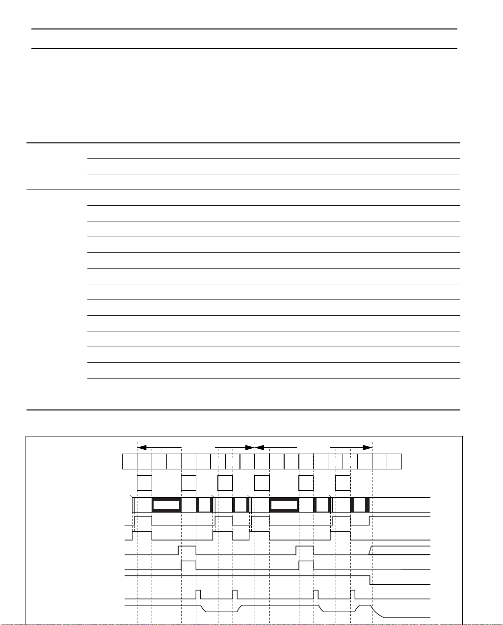
HD155111F
Power saving is implemented through use of the idle mode. All function blocks of the HD155111F are
switched off until such time as the system controller commends the device to power up again.
Table 1 Operating Modes with Power Saving
Receive
(Rx)
Calibrate
(Cal)
Warm-up
(Lo-ON)
Transmit
(Tx)
Idle
(PS)
Mode POONRX1 (pin 1) H L L L H
switch POONRX2 (pin 2) H H L L L
POONTX (pin 7) L L L H Don’t care
HD155111F LNA bias ON OFF OFF OFF OFF
circuit status 1st mixer ON OFF OFF OFF OFF
IF AMP ON ON OFF OFF OFF
2nd mixer ON ON OFF OFF OFF
AGC ON ON OFF OFF OFF
IO demodulator ON ON OFF OFF OFF
Divider (Rx.) ON ON OFF OFF OFF
Divider (Tx.) OFF OFF OFF ON OFF
IO modulator OFF OFF OFF ON OFF
Offset PLL OFF OFF OFF ON OFF
RF 1st local buffer ON ON ON ON OFF
IF local buffer ON ON ON ON OFF
IFVCO ON ON ON ON OFF
Total current 42.5 mA Typ 32 mA Typ 10.5 mA Typ 38 mA Typ 1 µA Typ
The slots of
PCN system
Operating modes
of the HD155111F
POONRX1(pin 1)
POONRX2(pin 2)
POONTX (pin 7)
Power Amplifier ON
UHF PLL synth. ON
UHF PLL synth. load
VCO control voltage
of UHF PLL synth.
4.615ms
7012345670123456701
Rx RxTx Tx
Cal Cal Cal Cal
Rx Rx Rx Rx
Tx Tx
Lo-ON Lo-ON
Mon Mon
LoON
LoON
4.615ms
LoON
Lo-
ON
Idle(PS) mode don't care
PS
Page 12
HD155111F
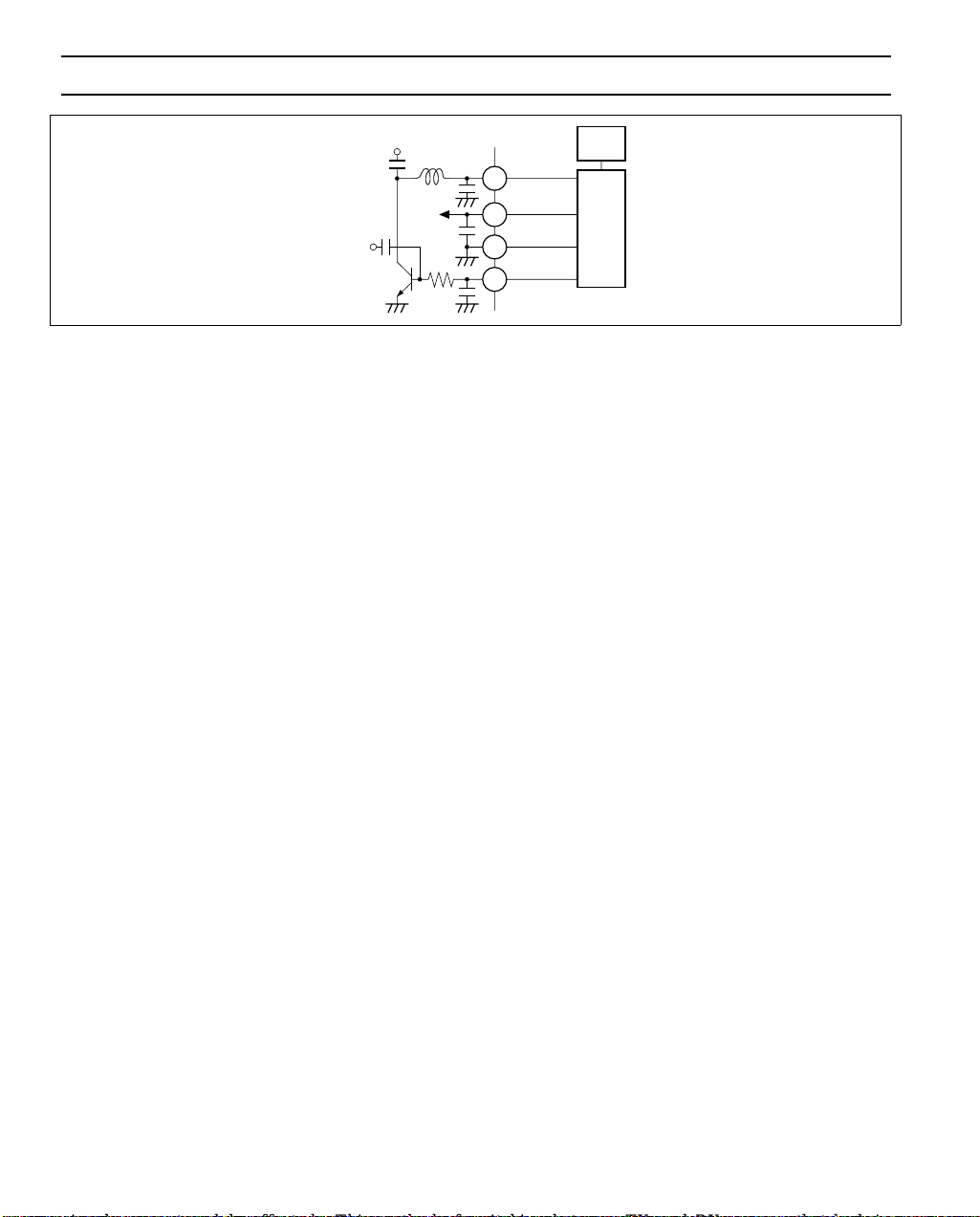
IFVCO Operation
The HD155111F incorporates an IFVCO circuit. The IFVCO circuit consists of an IFVCO transistor and a
bias circuit for it, whose current are 2.0 mA and 0.5 mA respectively. If an internal IFVCO is used, treat
pin 23 (IFVCOO), pin 24 (IFVCOI) and pin 21 (IFLO) as shown figure 3-(a).
Using an external IFVCO, pin 23 (IFVCOO) and pin 24 (IFVCOI) cannot be connected any pattern and
component, and any component to feed direct current must be also removed from pin 21 (IFLO).
If pin 23 (IFVCOO), pin 24 (IFVCOI) and pin 21 (IFLO) are treated as shown figure 3-(b), current
consumption will decrease 2.0 mA.
Moreover, there is the other external IFVCO solution using only an IFVCO bias circuit as shown figure 3(c). The IFVCO bias circuit has an internal power save function. Therefore, if figure 3-(c) is adopted, an
internal power save function can be used as well as figure 3-(a).
IFVCO
bias circuit
IFVCO
bias circuit
IFVCOI
HD155111F
IFVCOI
Vtune
IFLO
HD155111F
PLL
synth.
Vtune
IFLO
PLL
synth.
23
21 24
IFLO
IFVCOO
External
IFVCO
23
21 24
IFLO
IFVCOO
Vcc
(a) using an internal IFVCO (b) using an external IFVCO
23
21 24
IFLO
IFVCOO
Vcc
(c) using only an IFVCO bias circuit
Figure 3 IFVCO Circuits
IFVCO
bias circuit
HD155111F
IFVCOI
Vtune
IFLO
PLL
synth.
Page 13

HD155111F
Absolute Maximum Ratings
Any stresses in excess of the absolute maximum ratings can cause permanent damage to the HD155101BF.
Item Symbol Rating Unit
Power supply voltage (VCC) VCC –0.3 to +4.0 V
Power supply voltage (VCCCOMP) VCCCOMP –0.3 to +5.5 V
Pin voltage V
Maximum power dissipation P
Operating temperature Topr –20 to +75 °C
Storage temperature Tstg –55 to +125 °C
T
T
–0.3 to VCC + 0.3 (6.0 Max) V
400 mW
Page 14

HD155111F
Oco
C
C
Electrical Characteristics (Ta = 25°C)
Specifications
Item Symbol Min Typ Max Unit Test Conditions
Power supply voltage (1) V
Power supply voltage (2) V
Power supply current (Rx.) I
Power supply current (Tx.) I
Power supply current
CC
CCCOMP
CC(Rx.)
CC(Tx.)
I
CC(Lo-ON)
(Lo-ON)
Power saving mode supply
I
CC(PS)
current
Power up time (Rx.) t up
Power up time (Tx.) t up
Power on control voltage
range (Rx1, Rx2, Tx)
Vthon
Vthon
Vthon
Power off control voltage
range (RX1, Rx2, Tx)
Vthoff
Vthoff
Vthoff
I/Q common-mode output
voltage
I/Q differential output swing V
I/Q output offset voltage V
I/Q common-mode input
voltage
I/Q differential input swing V
V
I
V
QOcom
IOsw
V
QOsw
IOoffset
V
QOoffset
V
IIcom
V
QIcom
IIsw
V
QIsw
Note: ( ) : These data are actual spread, not guaranteed.
2.7 3.0 3.6 V 4, 8, 20, 31,
2.7 3.0 5.25 V 11
— 42.5 60.0 mA VCC = 3.0V
V
= 3.0V
CCCOMP
— 38.0 55.0 mA VCC = 3.0V
V
= 3.0V
CCCOMP
— 10.5 15.0 mA VCC = 3.0V
V
= 3.0V
CCCOMP
— 1.0 10.0 µAVCC = 3.0V
V
= 3.0V
CCCOMP
— 1.5 (5.0) µsec VCC = 3.0V
(Rx.)
— 0.2 (0.5) µsec VCC = 3.0V
(Tx.)
2.3 — — V VCC = 3.0V 1
RX1
RX2
TX
— — 0.8 V VCC = 3.0V 1
RX1
RX2
TX
/
1.1 1.3 1.5 V VCC = 3.0V 25, 26
m
/
2.4 3.0 — Vp-p VCC = 3.0V
/
–60 0 +60 mV VCC = 3.0V
/
(0.8) 1.0 (1.2) V VCC = 3.0V 14, 15
/
— 2.0 (2.4) Vp-p VCC = 3.0V
V
CCCOMP
V
CCCOMP
V
IOUT
V
QOUT
V
IOUTD
V
QOUTDC
V
IIN
V
QIN
– V
– V
– V
= 3.0V
= 3.0V
– V
– V
– V
IINB
QINB
IOUTB
QOUTB
IOUTBD
QOUTBDC
Applicable
pins Note
34, 41, 45
4, 8, 20, 31,
34, 41, 45, 11
4, 8, 20, 31,
34, 41, 45, 11
4, 8, 20, 31,
34, 41, 45, 11
4, 8, 20, 31,
34, 41, 45, 11
from PS
mode
from PS
mode
2
7
2
7
27, 28
25, 26
27, 28
25, 26
27, 28
16, 17
14, 15
16, 17
Page 15

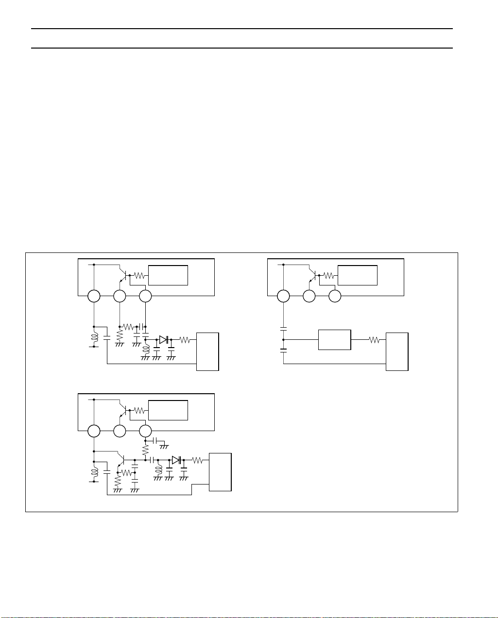
HD155111F
Block Specifications
• Specifications of BRIGHT LNA
Item Min Typ Max Unit Test Conditions
Frequency (RF) 1805 1840 1880 MHz
Power gain — 13.0 — dB RF = 1840MHz , Pin = –50dBm
Noise figure — 2.0 — dB RF = 1840MHz
i/p IP3 — –0.5 — dBm RF1 = 1840.8MHz, RF2 = 1841.6MHz
o/p IP3 — 12.5 — dBm RF1 = 1840.8MHz, RF2 = 1841.6MHz
i/p CP — –10.5 — dBm RF = 1840MHz
o/p CP — 1.4 — dBm RF = 1840MHz
Load Z — 50 — Ω 50Ω Typ
i/p Z — 50 — Ω 50Ω Typ
i/p VSWR — 1.5 — RF = 1840MHz, 50Ω
o/p VSWR — 1.5 — RF = 1840MHz, 50Ω
ICC @LNA Trs. 4.7 5.6 6.8 mA Only Trs. current
Note: These AC characteristics are shown for reference only and do not form part of the HD155111F
component specification.
• Specifications of BRIGHT Mixer 1 (Output Load = 400Ω + 400Ω balanced)
Item Min Typ Max Unit Test Conditions
Frequency (RF) 1805 1840 1880 MHz
Frequency (LO) 1505 1617 1750 MHz
Frequency (IF) (130) 225 (300) MHz
RFLO input level –10 — — dBm
Conversion gain 5.5 8.0 10.0 dB RF = 1840MHz/Pin = –50dBm,
LO = 1615MHz/Pin = –10dBm, IF = 225MHz
Noise figure (7.0) 9.0 (11.0) dB RF = 1840MHz,
LO = 1615MHz/Pin = –10dBm, IF = 225MHz
i/p IP3 (–8.0) –5.0 (–2.5) dBm RF1 = 1840.8MHz, RF2 = 1841.6MHz,
LO = 1615MHz/Pin = –10dBm
o/p IP3 (–2.0) 3.0 (7.0) dBm RF1 = 1840.8MHz, RF2 = 1841.6MHz,
LO = 1615MHz/Pin = –10dBm
i/p CP –16.5 –13.5 (–11.0) dBm RF = 1840MHz,
LO = 1615MHz/Pin = –10dBm, IF = 225MHz
o/p CP (–11.5) –6.5 (–2.5) dBm RF = 1840MHz,
LO = 1615MHz/Pin = –10dBm, IF = 225MHz
RF i/p VSWR — 1.5 (2.0) RF = 1840MHz, 50Ω
LO i/p VSWR — 1.5 (2.0) RF = 1615MHz, 50Ω
IF o/p VSWR — 1.5 (2.0) RF = 225MHz, 800Ω (400Ω + 400Ω Balanced)
Page 16

HD155111F
• Specifications of BRIGHT IFAmp + Mixer 2
Item Min Typ Max Unit Test Conditions
Input frequency (IF1) (130) 225 (300) MHz
Frequency (LO2) (156) 270 (360) MHz LO2 = IFLO/2
Output frequency (IF2) (26) 45 (60) MHz
IFLO input level –10 — — dBm
Conversion gain 9.0 12.0 14.5 dB IF1 = 225MHz/Pin = –40dBm,
IFLO = 540MHz/Pin = –10dBm, IF2 = 45MHz
Noise figure (4.5) 5.6 (7.0) dB IF1 = 225MHz,
IFLO = 540MHz/Pin = –10dBm, IF2 = 45MHz
i/p IP3 — –16.0 — dBm IF11 = 225.8MHz, IF2 = 226.6MHz,
IFLO = 540MHz/Pin = –10dBm
o/p IP3 — –4.0 — dBm IF11 = 225.8MHz, IF2 = 226.6MHz,
IFLO = 540MHz/Pin = –10dBm
i/p CP –27.5 –25 (–23.0) dBm IF1 = 225MHz,
IFLO = 540MHz/Pin = –10dBm, IF2 = 45MHz
o/p CP (–18.0) –14.0 (–11.0) dBm IF1 = 225MHz,
IFLO = 540MHz/Pin = –10dBm, IF2 = 45MHz
Isolation — 60 — dB Between mixer 1 outputs and IFAmp inputs
Note: ( ) : These data are actual spread, not guaranteed.
• Specifications of BRIGHT AGC
Item Min Typ Max Unit Test Conditions
Input frequency (26) 45 (60) MHz
Control voltage range 0.15 — 2.3 V
Gain range 89 98 107 dB Gain 1 – Gain 3
Gain linearity (–1.0) — (1.0) dB in any 20dB window
Gain 1 45 55 65 dB Vcont = 2.3V
Gain 2 13 23 33 dB Vcont = 1.5V
Gain 3 –55 –40 –35 dB Vcont = 0.15V
i/p CP 1 (–64) –59 — dBm Gain = 50dB
i/p CP 2 (–34) –29 — dBm Gain = 10dB
i/p CP 3 (–22) –17 — dBm Gain = –30dB
Note: ( ) : These data are actual spread, not guaranteed.
Page 17

HD155111F
• Specifications of BRIGHT IQ Demodulator
Item Min Typ Max Unit Test Conditions
Power gain –0.5 1.4 3.5 dB IF2 = 45MHz, Pin = –25dBm, Rout = 10kΩ,
IFLO = 540MHz, Pin = –10dBm
i/p CP (–17.5) –16.0 (–14.0) dBm IF2 = 45MHz, Baseband = 67.7kHz,
IFLO = 540MHz, Pin = –10dBm
o/p CP (–19.0) –15.6 (–12.0) dBm IF2 = 45MHz, Baseband = 67.7kHz,
IFLO = 540MHz, Pin = –10dBm
IQ phase accuracy –1.0 0 1.0 deg. Baseband = 67.7kHz
IQ amplitude mismatch (–0.5) 0.1 (0.5) dB Baseband = 67.7kHz
Output DC offset voltage –60 0 60 mV |IOUT – IOUTB| and |QOUT – QOUTB|
IQ differential output
swing
I/Q common mode
output voltage
Note: ( ) : These data are actual spread, not guaranteed.
2.4 3.0 — Vp-p Baseband = 67.7kHz
|IOUT – IOUTB| and |QOUT – QOUTB|
1.1 1.3 1.5 V VCC = 3.0V
Page 18

HD155111F
• Specifications of BRIGHT IQ Modulator and Offset PLL
Item Min Typ Max Unit Test Conditions (Loop bandwidth = 1.4MHz)
Frequency (RF) 1710 1747 1785 MHz
Frequency (LO) 1530 1612 1665 MHz
Frequency (IF) (120) 135 (180) MHz
Power up time — 0.3 (0.5) µsec from PS mode
Lock up time — 20 (80) µsec from PS mode to 1880MHz
IFLO input level –10 — — dBm
VCOIN input level –10 — — dBm
Carrier suppression ratio 31 40 — dBc All ‘1’ GMSK (Baseband = 67.7kHz)
Upper side-band
suppression ratio
Phase accuracy — 0.98 (2.5) deg. rms 200kHz Bandwidth
(PN9, GMSK) — 2.74 (6.0) deg. peak 200kHz Bandwidth
Modulation spurious — –36.0 (–33.0) dBc 200kHz offset / 30kHz Bandwidth
(PN9, GMSK) — –68.5 (–63.0) dBc 400kHz offset / 30kHz Bandwidth
Tx noise in RX band — –156 (–153) dBc/Hz 1805MHz to 20MHz up from Tx band
(Tx power = 0dBc = 30dBm) — –162 (–153) dBc/Hz 1850MHz to 65MHz up from Tx band
Isolation of the 1st local
input to TXVCO input
IQ differential input swing — 2.0 (2.4) Vp-p |IIN – IINB| and |QIN – QINB|
I/Q common mode input
voltage
Note: ( ) : These data are actual spread, not guaranteed.
35 45 — dBc I/Q differential input swing = 2.0Vp-p
I/Q common mode input voltage = 1.0V
— –73.0 (–63.0) dBc 600kHz to 1.8MHz offset / 30kHz Bandwidth
— –73.5 (–66.0) dBc 1.8MHz to 3MHz offset / 100kHz Bandwidth
— –75.5 (–68.0) dBc 3MHz to 6MHz offset / 100kHz Bandwidth
— –77.0 (–74.0) dBc 6MHz upwards offset / 100kHz Bandwidth
(40) 43 — dB
(0.8) 1.0 (1.2) V
Page 19

Test Circuit
HD155111F
R701
SMA
J702 (MIX2RF)
C805
SMA
J801 (MIX1IF)
C807
VCCJ803 (MIX1RF)
SMA
J802 (MIX1LO)
SMA
0
1000p
5
4
1000p
T801
617PT-1206
16
1
2
2
34
3
C808
C809
C811
4p
C813
3p
C706
7p
C803
1000p
100p
1000p
L802
J701 (MIX2IF/AGCIN)
C704
T701
C702
6p
C705
100n
L701
100n
L801
C801
C810
1000p
1.5n
2p
C812
3.3n
L803
SMA
C703
3300p
4
5
34216
321
617DB-1018
C701
1000p
3p
VCC
J601 (AGCOUT)
SMA
C610
3300p
C608
C609
3300p
3300p
4
5
T601
34216
321
617DB-1018
1000p
3635343332313029282726
MIX2OB
MIX2O
VCCAGC
GNDAGC
37
IFINB
38
IFIN
39
GNDIF
40
VCCIF
41
MIX1OUT
42
MIX1OUTB
43
RFLOIN
44
VCCMIX1
45
GNDMIX1
46
MIX1INB
47
MIX1IN
48
POONRX1
POONRX2
RFOUT
123456789
C202
10p
3.3n
L201
Q201
BPF420
C203
27p
3300p
C607
3300p
AGCOUT
AGCOUTB
VCCLNA
GNDLNA
R201
L202
VCC
VCCDIV
IC001
RFIN
C205
4.7k
C206
3.3n
C207
10p
0.5p
0.5p
VCONT
IOUT
IOUTB
QOUT
C606
47p
IOUT
QOUT
IOUTB
VCONT
GNDDIV
HD155111F
POONTX
VCCPLL
GNDPLL
VCOIN
VCCCOMP
101112
C301
47p
QOUTB
25
QOUTB
PLLOUT
C302
120p
C601
1000p
IFVCOI
IFVCOO
GNDIQ
IFLO
VCCIQ
MOD
MODB
IIN
IINB
QIN
QINB
CURAD
VTUNE
C508
2.7k
R502
C507
L502
HVU355
VARICAP1
C506
6p
C505
C503
24
23
22
21
20
19
18
17
16
15
14
13
22k
R307
VCC
C909
C908
C907
1000p
8p
8.2n
3p
6p
C303
VCCCOMP
100000n
C906
100n
C905
27p
C904
C504
3p
100
R501
C304
R304
R301
100p
VCCVCOEXT
100000n
C903
100n
C902
27p
C901
L501
0.75p
18
R303
0
R302
100000n
100n
27p
C502
1000p
15n
13p
C405
0
VCO1
0
VTUNE
POONRX1
POONRX2
POONTX
QINB
QIN
IINB
IIN
VCONT
QOUTB
QOUT
IOUT
IOUTB
120p
C501
C406
1000p
39n
L402
39n
L401
C305
1000p
R305
321
OUT VCC
456
Kv=11MHz/V
MQE601-902
MQE502-902 or
GND
26
VCC
25
VCCCOMP
24
POONRX
23
VCCVCOEXT
22
SLEEP
21
VTUNE
20
POONRX1
19
GND
18
POONRX2
17
GND
16
POONTX
15
QINB
14
QIN
13
IINB
12
GND
11
GND
10
IIN
9
VCONT
8
GND
7
QOUTB
6
GND
5
GND
4
QOUT
3
IOUT
2
IOUTB
1
SMA
J501 (IFLO)
VCC
IIN
IINB
QIN
QINB
C308
3300p
R306
130
C307
220p
220
GND GND
MOD CON
C201
SMA
2p
C204
1000p
SMA
SMA
Page 20

HD155111F
Measurement Results
LNA Measurement Results (for reference only)
Conditions:
Vcc = 3.0 V
POONRX1 (pin 1) = 3.0 V
POONRX2 (pin 2) = 3.0 V
POONTX (pin 7) = 0 V
50 Ω
Output(RF)
1000 p
Input(RF)
1840 MHz,
−50 dBm
50 Ω
20
15
10
3.0 V
1000 p
132 4 8 11 20 31 34 41 45
10 p
Rbias
100
Ic
6
5 7 9 22 30 35 40 46
TRS:
Siemens BFP420
2 p
3.3 n
3.3 n
0.5 p0.5 p
4.7 k
10 p
Figure 4 Evaluation Circuit for LNA
Vbias
0.56 V
Active bias circuit
HD155111F
3.5
3
2.5
5
Vcc=3.0V
0
Pin=−50dBm
Ta=27°C
−5
Gain [dB], ICP [dBm]
Gain [dB]
ICP [dBm]
NF [dB]
−10
−15
1780 1800 1820 1840 1860 1880 2000 2020
Frequency [MHz]
Figure 5 Gain, NF, ICP vs. Frequency
2
1.5
1
0.5
0
NF [dB]
Page 21

HD155111F
40
Vcc=3.0V
Freq.=1840MHz
20
0
−20
−40
Pout [dBm]
Interfere(1)=1840.8MHz
−60
Interfere(2)=1841.6MHz
Ta=27°C
−80
−100
−120
−60 −50 −40 −30 −20 −10 0 10
Pin [dBm]
Pout [dBm]
IM3 [dBm]
Gain [dB]
Figure 6 Gain, Pout vs. Pin
15
Freq.=18940MHz
Pin=−50dBm
14
15
14
13
12
11
10
9
8
7
Gain [dB]
13
Gain [dB]
12
11
10
2 2.5 3 3.5 4 4.5
Vcc [V]
−40
−20
27
80
100
Figure 7 Gain vs. Supply Voltage
Page 22

HD155111F
3
Freq.=1840MHz
2.5
2
1.5
NF [dB]
1
0.5
0
2 2.5 3 3.5 4 4.5
Vcc [V]
Figure 8 NF vs. Supply Voltage
−40
−20
27
80
100
−6
Freq.=1840MHz
−8
−10
−12
ICP [dBm]
−14
−16
2 2.5 3 3.5 4 4.5
Vcc [V]
Figure 9 ICP vs. Supply Voltage
−40
−20
27
80
100
Page 23

8
7.5
7
6.5
6
5.5
Icc@TRS [mA]
5
4.5
4
2 2.5 3 3.5 4 4.5
Vcc [V]
Figure 10 LNA Transistor Current vs. Supply Voltage
HD155111F
−40
−20
27
80
100
Page 24

HD155111F
1st Mixer Measurement Results
Conditions:
Vcc = 3.0 V
POONRX1 (pin 1) = 3.0 V
POONRX2 (pin 2) = 3.0 V
POONTX (pin 7) = 0 V
1615 MHz, −10 dBm
Input (LO)
Input (RF)
1840 MHz, −50 dBm
50 Ω
50 Ω
10
5
Load: 400 ohm Balanced
TOKO: 617PT-1206
800 Ω: 50 Ω
Insertion loss: 1.5 dB@225 MHz
Gilbert
Cell Mix
4 p
3 p
3.0 V
1000 p
1000 p
1.5 n
3.3 n
2 p
1
2 4 8 11 20 31 34 41 45
Lo Buff2
44
Lo Buff
47
48
5 7 9 22 30 35 40 46
Figure 11 Evaluation Circuit for 1st Mixer
43
42
Vcc
100 n
3 p
Output (IF)
1000 p
1000 p
225 MHz
50 Ω
16
14
Vcc=3.0V
Pin=-50dBm
0
Pin(LO)=−10dBm
Freq.IF=225MHz
C.G. [dB]
ICP [dBm]
NF SSB [dB]
Ta=27°C
-5
C.G. [dB], ICP [dBm]
-10
-15
1780 1800 1820 1840 1860 1880 1900 1920
Frequency [MHz]
Figure 12 Gain, NF, ICP vs. Frequency
12
10
8
6
NF SSB [dB]
Page 25

HD155111F
40
20
Interfere(1)=1840.8MHz
0
Interfere(2)=1841.6MHz
Ta=27°C
−20
−40
Pout [dBm]
Vcc=3.0V
Freq.RF=1840MHz
−60
Freq.LO=1615MHz
Pin(LO)=−10dBm
−80
Freq.IF=225MHz
−100
−120
−60 −50 −40 −30 −20 −10 0 10
Pin [dBm]
Pout [dBm]
IM3 [dBm]
Gain [dB]
Figure 13 Gain, Pout vs. Pin
10
8
7
8
7
6
5
4
3
2
25
C.Gain [dB]
5
Freq.RF=1840MHz
Freq.LO=1615MHz
0
−5
C.Gain [dB]
−10
−15
−60 −50 −40 −30 −20 −10 0 10
Plo [dBm]
Freq.IF=225MHz
Pin(RF)=−50dBm
Ta=27°C
NF SSB [dB]
C.Gain [dB]
Figure 14 CG, NF vs. Local Input Power
20
15
10
5
0
NF SSB [dB]
Page 26

HD155111F
C.Gain [dB]
10
Vcc=3.0V
Freq.LO=1615MHz
Pin(LO)=−10dBm
8
Pin(RF)=−50dBm
Ta=27°C
6
4
2
C.Gain [dB]
0
160 200 240 280180 220 260
Frequency [MHz]
Figure 15 Output Frequency Characteristics
10
9
8
7
6
5
4
C.Gain [dB]
3
2
1
0
2
−40
−20
27
80
100
2.5 3 3.5 4 4.5
Vcc [V]
Figure 16 Gain vs. Supply Voltage
Page 27

15
HD155111F
14
13
12
11
10
9
SSB NF [dB]
8
7
6
5
2
−12
−13
−40
−20
27
80
100
2.5 3 3.5 4 4.5
Vcc [V]
Figure 17 NF(SSB) vs. Supply Voltage
−14
−15
ICP [dBm]
−16
−17
−18
2 2.5 3 3.5 4 4.5
Vcc [V]
Figure 18 ICP vs. Supply Voltage
−40
−20
27
80
100
Page 28

HD155111F
IF AMP + 2nd Mixer Measurement Results
Conditions:
Vcc = 3.0 V
POONRX1 (pin 1) = 3.0 V
POONRX2 (pin 2) = 3.0 V
POONTX (pin 7) = 0 V
Input (1st IF)
225 MHz, −40 dBm
Input (IFLO)
540 MHz, −10 dBm
50 Ω
50 Ω
20
15
10
3.0 V
1000 p
9 p
0.01 µ
82 n
10 p
1
2 4 8 11 20 31 34 41 45
IF AMP
39
38
21
270 MHz
Divider
1/2
5 7 9 22 30 35 40 46
150
Mixer2
150
300
AGC
37
36
Output test-circuit
for IF AMP + Mixer2
evaluation only
1000 p
1000 p
200 Ω: 50 Ω
TOKO
617DB-1018
Insertion loss = 3.6 dB
Figure 19 Evaluation Circuit for IF AMP + 2nd Mixer
C.Gain
Pout_2IF
1dB
Output (MIX2)
1000 p
1000 p
0
−10
−20
45 MHz
5
C.Gain [dB]
0
ICP : −25dBm
−5
−70 −60 −50 −40 −30 −20 −10 0 10
Pin_RF [dBm]
Figure 20 Input-Output Characteristics, 1dB-Compression Point
−30
Pout_2IF [dBm]
−40
−50
Page 29

20.0
HD155111F
0.0
−20.0
−40.0
Pout [dBm]
−60.0
−80.0
−100.0
−60 −50 −40 −30 −20 −10 0
IP3out :−4.0dBm
Pout_IM3
Pout_2IF
IF11=225.8MHz
IF12=226.6MHz
IP3in :−16.0dBm
Pin_RF [dBm]
Figure 21 Intermodulation 3rd Characteristics
20
10
0
3.0V −40°C
−10
−20
C.Gain [dB]
−30
IF1=225MHz/Pin=−30dBm,
IFLO=540MHz,IF2=45MHz
3.0V 27°C
3.0V 100°C
−40
−50
−50 −40 −30 −20 −10 0 10
Local in [dBm]
Figure 22 C.Gain vs. Local in Power
Page 30

HD155111F
20
10
0
−10
C.Gain [dB]
−20
−30
2 2.5 3 3.5 4 4.5
C.Gain
−40°C
27°C
100°C
2.7V to 3.6V
NF SSB
Vcc [V]
Figure 23 C.Gain, NF SSB vs. Supply Voltage
−20
Vcc=4.0V
Vcc=3.0V
−22
Vcc=2.7V
25
20
15
10
5
0
NF SSB [dB]
−24
−26
−28
ICP(Input Compresion Point) [dBm]
IF1=225MHz,
IFLO=540MHz/Pin=−10dBm,IF2=45MHz
−30
−40 −20 0 20 40 60 80 100
Temperature [deg]
Figure 24 ICP vs. Temperature
Page 31

AGC Measurement Results
3.0 V
1000 p
45 MHz
50 Ω
1000 p
50 Ω: 200 Ω
1000 p
TOKO
617DB-1018
insertion loss = 3.6 dB
37
36
Figure 25 Evaluation Circuit for the AGC & Power On Control Blocks
1
2 4 8 11 20 31 34 41 45
150
300
POONRX1
POONRX2
control
5 7 9 22 30 35 40 46
Mixer2 output R
150
ATT AGC AMP
LinearizerPower on/off
IQ Demodulator
IF AMP + Mixer2
IF VCO
Divider
LNA & Mixer 1
Transmitter block
2 k
IQ Demo
2 k
33
32
29
HD155111F
Output test-circuit
for AGC block
evaluation only
Output (MIX2)
200 Ω: 50 Ω
3300 p
Vcont
0.15 to 2.3 V
Conditions:
Vcc = 3.0 V
POONRX1 (pin 1) = 3.0 V
POONRX2 (pin 2) = 3.0 V
POONTX (pin 7) = 0 V
45 MHz
3300 p
3300 p
TOKO
617DB-1018
insertion loss = 6.1 dB
80
Ta=−40°C
60
Ta=27°C
Ta=100°C
40
Vcc=3.0V,
Freq=45MHz,
20
Zin=300Ω
0
Gp [dB]
−20
−40
−60
0 0.5 1 1.5 2 2.5
Vcont [V]
Figure 26 Power Gain vs. Vcont Voltage
Page 32

HD155111F
GP [dB]
60
Ta=−40°C
55
50
45
40
Vcc=3.0V,
Vcont=2.3V,
Freq=45MHz,
35
Pin=−100dBm,
Zin=300Ω
30
10 10020 50
Ta=27°C
Ta=100°C
Frequency [MHz]
Figure 27 Power Gain vs. Frequency
60
Vcc=3V, freq.=45MHz
50
40
Ta=−40°C
Ta=27°C
Ta=100°C
30
NF [dB]
20
10
0
−40 −200 20406080
Gp [dB]
Figure 28 Noise Figure(NF) vs. Power Gain(Gp)
Page 33

10
HD155111F
0
−10
−20
−30
ICP [dBm]
−40
−50
−60
−70
−40 −20 0 20 40 60
Gp [dB]
VCC=3V, freq.=45MHz
Ta=−40°C
Ta=27°C
Ta=100°C
Figure 29 Input Compression Point(ICP) vs. Power Gain(Gp)
60
40
20
0
−20
Gp [dB]
Freq=45MHz,
Zin=300Ω
Ta=−40@Vcont=2.3
Ta=27@Vcont=2.3
Ta=100@Vcont=2.3
Ta=−40@Vcont=0.15
Ta=27@Vcont=0.15
Ta=100@Vcont=0.15
−40
−60
−80
1.5 2 2.5 3 3.5 4 4.5
Vcc [V]
Figure 30 Power Gain(Gp) vs. Supply Voltage(Vcc)
Page 34

HD155111F
IQ Demodulator Measurement Results
3.0 V
1000 p
1
2 4 8 11 20 31 34 41 45
45 MHz
50 Ω
3300 p
3300 p
Input (IFLO)
540 MHz, −10 dBm
TOKO
617DB-1018
50 Ω: 200 Ω
3300 p
50 Ω
0.01 µ
33
32
21
Figure 31 Evaluation Circuit for the I&Q Demodulator Block
AGC
2 k
divider
÷6
2 k
90 MHz
(90° phase shifter)
5 7 9 22 30 35 40 46
45 MHz
÷2
2nd order
Butterworth filter
2nd order
Butterworth filter
10 k
10 k
Conditions:
Vcc = 3.0 V
POONRX1 (pin 1) = 3.0 V
POONRX2 (pin 2) = 3.0 V
POONTX (pin 7) = 0 V
IOUT
28
IOUTB
27
QOUT
26
25
QOUTB
Single ended 1kΩ input impedance
Single ended 10kΩ load impedance
V
V
10 k
10 k
10 k
10 k
Page 35

HD155111F
−10
−15
−20
OCP:-15.0dBm
Output[dBm] Vcc=3.0V
Output[dBm] Vcc=2.7V
Output[dBm] Vcc=3.6V
Ta = 25°C
1dB
−25
Gp[dB] Vcc=3.0V
−30
Output [dBm] (Single ended)
−35
Gp[dB] Vcc=2.7V
Gp[dB] Vcc=3.6V
ICP:-15.5dBm
−35 −30 −25 −20 −15 −10 −50
Input [dBm] (Single ended)
Figure 32 Input-Output Characteristics
−10
Output[dBm] Ta=25°C
−15
Output[dBm] Ta=−20°C
Output[dBm] Ta=80°C
30
20
10
0
−10
−20
30
20
Gp [dB]
−20
Vcc = 3V
−25
−30
Output [dBm] (Single ended)
Gp[dB] Ta=25°C
Gp[dB] Ta=−20°C
Gp[dB] Ta=80°C
−35
−35 −30 −25 −20 −15 −10 −50
Input [dBm] (Single ended)
Figure 33 Input-Output Characteristics
10
Gp [dB]
−10
−20
Page 36

HD155111F
f1: 45.8MHz
f2: 46.6MHz
0
OIP3: −0.2dBm
−10
−20
−30
GMSK
modulated signal
(All 1 GMSK)
+
DIV
(45MHz)
DEM
(67.7kHz)
−40
Output [dBm] (Single ended)
−50
−35 −30 −25 −20 −15 −10 −50
Output [dBm]
IM3 [dBm]
IIP3: −2.7dBm
Input [dBm] (Single ended)
Figure 34 Inter Modulation 3rd Characteristics
Rejection
@200k
@400k
@600k
@800k
@1600k
@3000k
@20000k
20
0
−20
−40
spec.(Min)
−0.3dB
−4.0dB
−9.4dB
−14.0dB
−25.9dB
−36.8dB
−50.0dB
fc: 210kHz
Iout
−2.6dB
−11.5dB
−21.3dB
−29.0dB
−43.3dB
−42.2dB
−54.7dB
Qout
−2.4dB
−11.2dB
−21.1dB
−28.7dB
−43.0dB
−42.0dB
−56.1dB
spec.1
spec.2
Iout
Qout
Rejection level [dB]
−60
−80
10 100 1000 10
4
10
5
Page 37

0.09[degree] 0.1[dB]
b) I&Q amplitude mismatcha) I&Q phase accuracy
HD155111F
1.38[V]
3.00[Vp-p]
c) common mode voltage
d) differential output swing
Figure 36 Demodulator Output Waveforms (67.7 kHz) at Vcc = 3.0 V, Ta = 25°C
Page 38

HD155111F
Transmitter Measurement Results
Input(LO),−10dBm
1575 to 1650MHz
Spectrum
analyzer
50 Ω
GMSK RF
TX. signal
1710 to 1785MHz
MURATA MQE520-1747
Kv=30MHz/V
C3=100pF
loop band width=1.5MHz
50 Ω
1000p
Conditions:
Vcc = 3.0 V
POONRX1 (pin 1) = 0 V
POONRX2 (pin 2) = 0 V
POONTX (pin 7) = 3.0 V
3300p
VCO
5.0V
R3
220
C2
R
18
R2
130
ICURAD
22k
1000 p4 p
RFLOIN
1.5n
0.75 p
VCCCOMP
PLLOUT
ICURAD
VCOIN
1000p
C1
220p
14
10
11
12
13
3.0 V
1000 p
1 2 4 8 20 31 34 41 45
LO buffer
VCO buffer
on
off
SW1
Power save control
POONTX=H, SW1=Off
5
7 9 22 30 35 40 46 16 17 2115141918
Low pass
I1I3
I2
Charge Pump
(Current mode driver)
Vcc
filter
Phase detector
1st. local signal
1575 to 1650 MHz
Down-converter
(offset mixer)
135 MHz
GMSK modulated IF
135 MHz
Low
pass
filter
MODB
39n
fo=135MHz
I&Q baseband
signal generator
I&Q modulator block
÷2
(90° phase shifter)
QIN
MOD
QINB
13p
39n
Q baseband signal
100 kHz
I baseband signal
100 kHz
IIN
IINB
0.01µ
50Ω
IFLO
Input(IFLO)
540MHz,
−10dBm
Figure 37 Evaluation Circuit for the Upconverter (I&Q Modulator and Offset PLL Block)
5
4
3
2
I1 peak, I2 peak, I3 [mA]
1
0
2 4 6 8 10 20
R
[kΩ]
I1 peak
I2 peak
I3
30
Page 39

HD155111F
Transmitter Measurement Results (1) (R
50Ω
VCO
MURATA
MQE502-902
18
220
VCC
VCCCOMP
Spectrum
Analyzer
VCCVCO
4.7V
Input(LO)
−10dBm
1575 to 1650MHz
+
0.01µ
33µ
3V
+
0.01µ
33µ
5V
50Ω
+
0.01µ33µ
= 22 kΩ and IFLO generated by signal generator)
ICURAD
VCC
1000p 15p
47
10
11
12
0.75p100p
130
3300p
4847464544434241403938
MIX1IN
1
POONRX1
2
POONRX2
3
RFOUT
4
VCCLNA
5
GNDLNA
6
RFIN
7
POONTX
8
VCCPLL
9
GNDPLL
VCOIN
VCCCOMP
PLLOUT
CURAD
1314151617181920212223
R
ICURAD
22k
I&Q baseband
Signal Generator
220p
00
0.01µ
RFLOIN
MIX1INB
VCCMIX1
GNDMIX1
HD155111F
QINB
QIN
IINB
IIN
13p
VCC
MIX1OUT
MIX1OUTB
MODB
MOD
39n39n
0.01µ
0.01µ
VCCIF
VCCIQ
GNDIF
IFLO
IFIN
GNDIQ
37
IFINB
MIX2O
MIX2OB
GNDAGC
VCCAGC
AGCOUT
AGCOUTB
VCCDIV
GNDDIV
VCONT
QOUTB
IFVCOO
IFVCOI
24
0.01µ
IOUT
IOUTB
QOUT
36
35
34
33
32
31
30
29
28
27
26
25
50Ω
0.01µ
0
0
0.01µ
Input(IFLO)
−10dBm
540MHz
VCC
Figure 39 Evaluation Circuit Using Signal Generator for the I&Q Modulator and Offset PLL
Table 2 Measurement Results Using SG (R
Item Spec. Measured1 Measured2 Measured3 Unit
Measured frequency 1710 1747 1785 MHz
200 kHz offset ≤ –33 –36.54 –36.25 –36.42 dBc
400 kHz offset ≤ –63 –67.16 –67.28 –67.43 dBc
600 kHz to 1.8 MHz offset ≤ –63 –71.44 –71.48 –71.67 dBc
1.8 MHz to 3 MHz offset ≤ –66 –73.32 –73.33 –73.44 dBc
3 MHz to 6 MHz offset ≤ –68 –75.32 –75.09 –75.20 dBc
6 MHz upwards offset ≤ –74 –76.01 –75.95 –75.98 dBc
Carrier suppression ≥ 31 45.13 45.13 45.13 dBc
Side band suppression ≥ 35 41.89 41.93 41.93 dBc
Phase accuracy PN9 ≤ 2.5 0.95 0.96 0.96 deg. rms
PN9 ≤ 6.0 2.49 2.42 2.39 deg. peak
All ‘1’ ≤ 2.5 0.81 0.80 0.80 deg. rms
All ‘1’ ≤ 6.0 1.97 1.94 1.95 deg. peak
= 22 kΩ, IFLO generated by signal generator)
ICURAD
Page 40

HD155111F
a-1. Spectrum1(1710MHz,PN9) a-2. Spectrum2(1710MHz,PN9)
b-1. Spectrum1(1747MHz,PN9) b-2. Spectrum2(1747MHz,PN9)
c-1. Spectrum1(1785MHz,PN9) c-2. Spectrum2(1785MHz,PN9)
Figure 40 GMSK Modulated Transmitter Output Spectrum (1710 MHz, 1747 MHz, 1785 MHz)
Page 41

HD155111F
T = –40°C 1747MHz, PN9 T = –40°C 1747MHz, PN9
T =
T =
1747MHz, PN9
°C
1747MHz, PN9
°C
T = °C
T = °C
1747MHz, PN9
1747MHz, PN9
Figure 41 GMSK Modulated Transmitter Output Spectrum vs. Temperature
Page 42

HD155111F
The Acquisition response of OPLL using 22 k Ω icurad is shown below. The control voltage of the VCO
was observed by the digital storage oscilloscope.
0.5V/div
.8us
a. from PS mode to 1747MHz lock
Figure 42 Acquisition Time (Lock Up Time)
us/div
0.5V/div
us
us/div
b. from PS mode to 1785MHz lock
Page 43

Package Dimesions
9.0 ± 0.2
0.21 ± 0.05
0.19 ± 0.04
9.0 ± 0.2
7.0
36 25
37
48
24
13
0.5
112
M
0.08
0.75 0.75
1.70 Max
1.40
0.17 ± 0.05
0.15 ± 0.04
HD155111F
Unit: mm
1.00
0° − 8°
0.10
Dimension including the plating thickness
Base material dimension
0.10 ± 0.07
0.50 ± 0.10
Hitachi Code
JEDEC
EIAJ
Weight
(reference value)
FP-48
Conforms
0.2 g
Page 44

HD155111F
Cautions
1. Hitachi neither warrants nor grants licenses of any rights of Hitachi’s or any third party’s patent,
copyright, trademark, or other intellectual property rights for information contained in this document.
Hitachi bears no responsibility for problems that may arise with third party’s rights, including
intellectual property rights, in connection with use of the information contained in this document.
2. Products and product specifications may be subject to change without notice. Confirm that you have
received the latest product standards or specifications before final design, purchase or use.
3. Hitachi makes every attempt to ensure that its products are of high quality and reliability. However,
contact Hitachi’s sales office before using the product in an application that demands especially high
quality and reliability or where its failure or malfunction may directly threaten human life or cause risk
of bodily injury, such as aerospace, aeronautics, nuclear power, combustion control, transportation,
traffic, safety equipment or medical equipment for life support.
4. Design your application so that the product is used within the ranges guaranteed by Hitachi particularly
for maximum rating, operating supply voltage range, heat radiation characteristics, installation
conditions and other characteristics. Hitachi bears no responsibility for failure or damage when used
beyond the guaranteed ranges. Even within the guaranteed ranges, consider normally foreseeable
failure rates or failure modes in semiconductor devices and employ systemic measures such as failsafes, so that the equipment incorporating Hitachi product does not cause bodily injury, fire or other
consequential damage due to operation of the Hitachi product.
5. This product is not designed to be radiation resistant.
6. No one is permitted to reproduce or duplicate, in any form, the whole or part of this document without
written approval from Hitachi.
7. Contact Hitachi’s sales office for any questions regarding this document or Hitachi semiconductor
products.
Hitachi, Ltd.
Semiconductor & IC Div.
Nippon Bldg., 2-6-2, Ohte-machi, Chiyoda-ku, Tokyo 100-0004, Japan
Tel: Tokyo (03) 3270-2111 Fax: (03) 3270-5109
URL NorthAmerica : http:semiconductor.hitachi.com/
For further information write to:
Hitachi Semiconductor
(America) Inc.
2000 Sierra Point Parkway
Brisbane, CA 94005-1897
Tel: <1> (800) 285-1601
Fax: <1> (303) 297-0447
Europe : http://www.hitachi-eu.com/hel/ecg
Asia (Singapore) : http://www.has.hitachi.com.sg/grp3/sicd/index.htm
Asia (Taiwan) : http://www.hitachi.com.tw/E/Product/SICD_Frame.htm
Asia (HongKong) : http://www.hitachi.com.hk/eng/bo/grp3/index.htm
Japan : http://www.hitachi.co.jp/Sicd/indx.htm
Hitachi Europe GmbH
Electronic components Group
Dornacher Straße 3
D-85622 Feldkirchen, Munich
Germany
Tel: <49> (89) 9 9180-0
Fax: <49> (89) 9 29 30 00
Hitachi Europe Ltd.
Electronic Components Group.
Whitebrook Park
Lower Cookham Road
Maidenhead
Berkshire SL6 8YA, United Kingdom
Hitachi Asia Pte. Ltd.
16 Collyer Quay #20-00
Hitachi Tower
Singapore 049318
Tel: 535-2100
Fax: 535-1533
Hitachi Asia Ltd.
Taipei Branch Office
3F, Hung Kuo Building. No.167,
Tun-Hwa North Road, Taipei (105)
Tel: <886> (2) 2718-3666
Fax: <886> (2) 2718-8180
Hitachi Asia (Hong Kong) Ltd.
Group III (Electronic Components)
7/F., North Tower, World Finance Centre,
Harbour City, Canton Road, Tsim Sha Tsui,
Kowloon, Hong Kong
Tel: <852> (2) 735 9218
Fax: <852> (2) 730 0281
Telex: 40815 HITEC HX
 Loading...